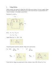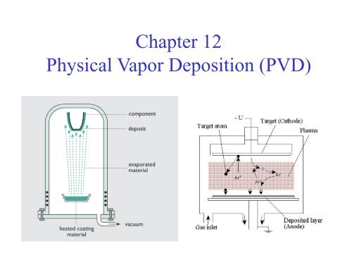
Chapter 12 Physical Vapor Deposition (PVD)
Chapter 12 Physical Vapor Deposition (PVD)
Chapter 12 Physical Vapor Deposition (PVD)

Create successful ePaper yourself
Turn your PDF publications into a flip-book with our unique Google optimized e-Paper software.
<strong>Chapter</strong> <strong>12</strong><br />
<strong>Physical</strong> <strong>Vapor</strong> <strong>Deposition</strong> (<strong>PVD</strong>)
<strong>PVD</strong> methods:<br />
Evaporation – condensation of metal vapor in<br />
high vacuum to deposit a thin film on a wafer; unable to<br />
cover severe topology (poor step coverage) which is<br />
beneficial when doing lift-off patterning; also hard to<br />
deposit alloys due to possible difference in melting<br />
points.<br />
Sputtering - use of plasma and acceleration of<br />
ions towards a target; material “sputtered” from the<br />
target and deposited on the wafer; extensively used in Si<br />
technology; moderate step coverage.
Evaporation Process:<br />
*Chamber under high vacuum (low pressure and long mfp)<br />
*metal pieces placed in crucible (charge) and heated to T m<br />
*substrates placed above the crucible, and<br />
*metal deposits on the substrates.<br />
Not shown in picture is a shutter that would be<br />
opened when the evaporation rate reaches a certain<br />
rate indicating pure metal deposition.<br />
View factor associated with deposition (like RTP);<br />
deposition rate depends on location of wafer in<br />
chamber (above crucible will have ↑ dep rate).<br />
For better uniformity and step coverage, planetary<br />
sample holders are rotated during deposition and<br />
samples are heated.<br />
<strong>Deposition</strong> rate monitored with quartz crystal<br />
(oscillates at a resonance frequency that shifts when<br />
additional mass is deposited on the crystal).<br />
Figure <strong>12</strong>.1 A simple diffusion-pumped<br />
evaporator showing vacuum plumbing and<br />
the location of the charge-containing<br />
crucible and the wafers.
For reasonable deposition<br />
rates, the vapor pressure<br />
must be ∼ 10 mTorr. This<br />
makes it nearly impossible<br />
ibl<br />
to evaporate some<br />
materials (refractory<br />
metals: Ta, W, Mo, Ti)<br />
Figure <strong>12</strong>.2 <strong>Vapor</strong> pressure curves for some commonly<br />
evaporated materials (data adapted from Alcock et al.).
<strong>Deposition</strong> rate depends on position of wafer<br />
View factor, k depends on R, Θ, Φ<br />
Wafers directly above the crucible will be coated more heavily than<br />
wafers off to the side. Wafers can all be mounted on the surface of a<br />
sphere (planetary) for more uniform deposition.<br />
Figure <strong>12</strong>.3 The geometry of deposition for a wafer (A) in an arbitrary<br />
position and (B) on the surface of a sphere.
Step Coverage<br />
If the substrate surface is not<br />
planar, the long mfp in<br />
evaporation means that<br />
evaporated material will follow<br />
a straight line; some areas are<br />
“shadowed”<br />
AR = step height<br />
step diameter<br />
Helps to rotate and heat the<br />
substrates.<br />
Planetary holders rotate<br />
simultaneously around two<br />
axes.<br />
Figure <strong>12</strong>.5 (A) Time evolution of the evaporative<br />
coating of a feature with aspect ratio of 1.0, with<br />
little surface atom mobility (i.e., low substrate<br />
temperature) and no rotation. (B) Final profile of<br />
deposition on rotated and heated substrates.
Evaporator systems: crucible heating techniques<br />
Resistively Heated<br />
Figure <strong>12</strong>.7 Resistive evaporator sources. (A) Simple sources including heating<br />
the charge itself and using a coil of refractory metal heater coil and a charge rod.<br />
(B) More standard thermal sources including a dimpled boat in resistive media.
Evaporator systems: crucible heating techniques<br />
Inductively Heated<br />
Figure <strong>12</strong>.8 Example of an inductively heated crucible used to create moderately<br />
charged temperatures.
Evaporator systems: crucible heating techniques<br />
Electron beam<br />
Heat of vaporization is<br />
supplied by the impact<br />
of an electron beam<br />
focused on the charge<br />
and melts a region of the<br />
material to be<br />
evaporated;<br />
Adv: possible to coevaporate<br />
materials with<br />
dual targets,<br />
Disadv: more expensive<br />
than resistance heated<br />
systems, substrates may<br />
have radiation damage<br />
Figure <strong>12</strong>.9 Electron beam evaporative sources. (A) A simple low flux<br />
source using a hot wire electron source and a thin movable rod. (B) A<br />
popular p source using a 2707 source arc in which the beam can be rastered<br />
across the surface of the charge. The magnet must be much larger than<br />
shown to achieve the full 270° of arc.
Evaporation<br />
Advantages: Simple process, relatively<br />
inexpensive, high purity films can be<br />
deposited.<br />
Disadvantages: difficult to evaporate alloys<br />
due to different melting points, “line of<br />
sight” deposition results in poor surface<br />
coverage unless there is rotation ti of fthe<br />
samples; deposition of refractory materials<br />
is a problem due to high temperatures<br />
required.<br />
Figure <strong>12</strong>.10 A commercial evaporator. Inset<br />
shows a planetary (photographs courtesy of<br />
CHA Industries).
Evaporation of Alloys<br />
Figure <strong>12</strong>.11 Methods for evaporating multicomponent films include (A)<br />
single-source evaporation, (B) multisource simultaneous evaporation, and (C)<br />
multisource sequential evaporation.
Sputtering:<br />
Bombard the target (cathode) with energetic ions, usually Ar + , in a<br />
plasma. Target material, not the wafers, must be placed on the electrode<br />
with maximum ion flux.<br />
*Chamber base pressure - high<br />
vacuum,<br />
*Argon flows into chamber<br />
raising pressure to mTorr range,<br />
*power supplied to electrodes,<br />
*target material deposits on the<br />
wafers.<br />
Allows deposition of refractory<br />
metals, alloys, dielectrics if an RF<br />
system is used.<br />
Figure <strong>12</strong>.<strong>12</strong> Chamber for a simple parallel-plateplate<br />
sputtering system.
Basic steps in sputter deposition:<br />
1) plasma generation – glow discharge formed when inert gas<br />
becomes ionized by an E-field; an electron accelerated towards<br />
anode, ionizes Ar atoms upon collision<br />
2) ion bombardment – Ar + impacts the target with high energies and<br />
transfer their momentum to the target material; these collisions<br />
disrupt the atomic surface causing target atoms, ions, and electrons to<br />
be ejected<br />
3) sputtered atom transport – sputtered atoms, ions, are influenced<br />
by collisions they undergo during transport to the film (determined<br />
by background pressure); sputtered particles will lose their energy as<br />
number of collisions increases so important to control the pressure<br />
4) film growth - sputtered material leaves the target and deposits on<br />
surrounding surfaces. The rate of diffusion is dependent upon the<br />
substrate material and Temp. Growth proceeds by diffusion and form<br />
nuclei, linuclei ligrow and eventually form islands; il islands il grow<br />
together until a continuous film is formed.
When an energetic ion strikes the surface of a material --<br />
1) Ions with low energies may bounce of the surface<br />
2) Ions may adsorb to the surface, giving up its energy to<br />
phonons (heat)<br />
3) Ion penetrates t into material, depositing energy deep into the<br />
substrate<br />
Figure <strong>12</strong>.13 Possible outcomes for an ion<br />
incident on the surface of a wafer.
Sputter Yield (S)<br />
Determines rate of sputter deposition<br />
S = # target atoms ejected/number of<br />
ions incident<br />
Depends on:<br />
•Target material<br />
•Mass of bombarding ions<br />
•Energy of bombarding ions<br />
Each target material has a threshold<br />
energy (below that energy no<br />
sputtering occurs), typically 10-30 eV.<br />
Figure <strong>12</strong>.14 Sputter yield as a function of ion<br />
energy for normal incidence id argon ions for a<br />
variety of materials (after Anderson and Bay,<br />
reprinted by permission).
S versus Ion atomic number<br />
Figure <strong>12</strong>.15 Sputter yield as a function of the bombarding ion<br />
atomic number for 45-keV ions incident on silver, copper, and<br />
tantalum targets (after Wehner, reprinted by permission, AIP).
Magnetron Sputtering – a magnetic field applied at right angles to<br />
the E-field; causes e- to follow spiral paths, increases probability of<br />
ionizing a gas atom, increases ionization efficiency, confines<br />
plasma resulting in a higher deposition rate; also able to form<br />
plasma at lower chamber pressures<br />
Figure <strong>12</strong>.17 Planar and cylindrical magnetron sputtering systems T: target; P:<br />
plasma; SM: solenoid; M: magnet; E: electric field; B: magnetic field (after<br />
Wasa and Hayakawa, reprinted by permission, Noyes Publications).
Fig. <strong>12</strong>.18 in text, p. 340 shows cross section of a planar magnetron<br />
target using permanent magnets to supply the field<br />
The region of the target beneath the ringshaped<br />
volume where the plasma density is<br />
highest is sputtered the most rapidly and this<br />
target erosion is called the race-track<br />
Target showing erosion in the race-track<br />
From: Fundamentals of High Power Impulse<br />
Magnetron Sputtering, dissertation by Johan Böhlmark<br />
Figure <strong>12</strong>.18 Detailed cross section of a<br />
rectangular planar magnetron target using<br />
permanent magnets to supply the field (after<br />
Wasa and Hayakawa, reprinted by<br />
permission, Noyes Publications).
Film morphology<br />
Zone model (Zones 1, 2, 3, T) indicates the films final<br />
characteristics based on the substrate temperature and ion energy;<br />
T-region is characterized by very small grains<br />
Zone1-low T, low ion energy<br />
yields amorphous, porous<br />
materials; Raise T or lower P<br />
moves to T-zone<br />
Zone2-Increase T and/or<br />
increase ion energy will<br />
increase grain size - tall<br />
columnar grains<br />
Zone3-Increase T, film has<br />
large 3-D grains– surface may<br />
be rough and hazy<br />
Figure <strong>12</strong>.21 The three-zone model of film deposition as proposed by<br />
Movchan and Demchishin (after Thornton, reprinted by permission, AIP).
Step Coverage<br />
Application of substrate heat will dramatically improve the step<br />
coverage due to surface diffusion; High AR can be a problem<br />
otherwise.<br />
Figure <strong>12</strong>.22 Cross section of the time evolution of the typical<br />
step coverage for unheated sputter deposition in a high aspect<br />
ratio contact.
Can improve step coverage by collimated sputtering or<br />
application of a bias to the wafer.<br />
Figure <strong>12</strong>.24 In collimated sputtering a<br />
disposable collimator is placed close to the<br />
wafers to increase directionality.<br />
Figure <strong>12</strong>.26 In bias sputtering, the ions<br />
incident on the surface of the wafer<br />
redistribute the deposited film to improve<br />
step coverage.
Ionized Metal Plasma (IMP) sputter deposition – ejected<br />
atoms pass through a second plasma; IMP process produces<br />
near-vertical deposition.<br />
Figure <strong>12</strong>.25 The Endura system by Applied Materials uses a number of <strong>PVD</strong> or CVD chambers<br />
fed by a central robot. For conventional and IMP sputtering, targets are hinged to open upward. Two<br />
open chambers are shown, along with the load lock (from Applied Materials).
Reactive sputtering: use of reactive gases (O 2 , CH 4 , NH 3 , N 2 ) rather<br />
than inert gases to sputter oxides, carbide, nitrides.<br />
Example below is for TiN<br />
Figure <strong>12</strong>.28 Resistivity and composition of reactively sputtered TiN as a function of the N 2<br />
flow in the sputtering chamber (after Tsai, Fair, and Hodul, reprinted by permission, The<br />
Electrochemical Society, and Molarius and Orpana, reprinted by permission, Kluwer<br />
Academic Publishing).
Figure <strong>12</strong>.29 Cross section electron micrograph of a<br />
moderately high aspect ratio contact that has been sputterdeposited<br />
with TiN (after Kohlhase, Mändl, and Pamler,<br />
reprinted by permission, AIP).
A thin film deposited on a substrate can be either in tensile stress or<br />
compressive stress; if stress is too large, film may peel away from<br />
the surface; implications in reliability.<br />
Figure <strong>12</strong>.30 The change in wafer deflection may be used to<br />
measure the stress in a deposited layer. This is typically measured<br />
using a reflected laser beam.
Sputtering<br />
Advantages: Moderately ygood step coverage; ;preferred<br />
technique for deposition of alloys, can sputter a wide variety of<br />
materials<br />
Disadvantages: may have some Argon incorporation in the film;<br />
could have some damage to substrate although not as much as in<br />
e-beam evaporation