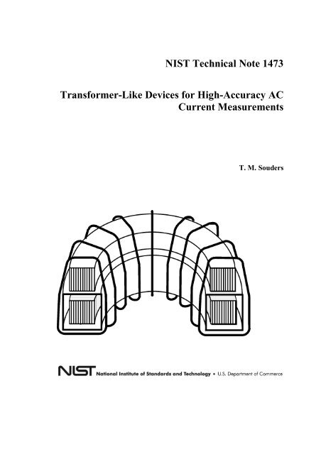
NIST Technical Note 1473 Transformer-Like Devices for High ...
NIST Technical Note 1473 Transformer-Like Devices for High ...
NIST Technical Note 1473 Transformer-Like Devices for High ...

Create successful ePaper yourself
Turn your PDF publications into a flip-book with our unique Google optimized e-Paper software.
<strong>NIST</strong> <strong>Technical</strong> <strong>Note</strong> <strong>1473</strong><br />
<strong>Trans<strong>for</strong>mer</strong>-<strong>Like</strong> <strong>Devices</strong> <strong>for</strong> <strong>High</strong>-Accuracy AC<br />
Current Measurements<br />
T. M. Souders
<strong>NIST</strong> <strong>Technical</strong> <strong>Note</strong> <strong>1473</strong><br />
<strong>Trans<strong>for</strong>mer</strong>-<strong>Like</strong> <strong>Devices</strong> <strong>for</strong> <strong>High</strong>-Accuracy AC<br />
Current Measurements<br />
T. M. Souders<br />
June 2008<br />
U.S. Department of Commerce<br />
Carlos M. Gutierrez, Secretary<br />
National Institute of Standards and Technology<br />
James M. Turner, Deputy Director
Certain commercial entities, equipment, or materials may be identified in this<br />
document in order to describe an experimental procedure or concept adequately. Such<br />
identification is not intended to imply recommendation or endorsement by the<br />
National Institute of Standards and Technology, nor is it intended to imply that the<br />
entities, materials, or equipment are necessarily the best available <strong>for</strong> the purpose.<br />
National Institute of Standards and Technology Special Publication <strong>1473</strong><br />
Natl. Inst. Stand. Technol. Spec. Publ. <strong>1473</strong>, 62 pages (June 2008)<br />
CODEN: NSPUE2
Table of Contents<br />
FOREWORD ………………………….……………….……………………………….. ix<br />
ABSTRACT ………………………………………………………………………………1<br />
1. INTRODUCTION…………………….………………………………………….….…… 2<br />
1.1 The Ideal <strong>Trans<strong>for</strong>mer</strong> ………………………………………………………………2<br />
1.2 <strong>Trans<strong>for</strong>mer</strong> Error and its Representation ……….………………………………….2<br />
1.3 Other Error Sources …………………………………………………………………3<br />
1.4 Notation………………………………………………………………………....….. 4<br />
2. PHYSICAL INTERPRETATION OF TRANSFORMER ERROR ……………………...4<br />
3. THE CURRENT COMPARATOR …………………………….…………………..….….7<br />
3.1 The Compensated Current Comparator …………………………………………... 10<br />
4. MAGNETIC DESIGN EQUATIONS AND THE<br />
MEASUREMENT OF MAGNETIC PROPERTIES………….…………………….….. 11<br />
4.1 Hysteresis, Permeability and Core Loss ………………………………………..… 11<br />
4.2 Magnetic Flux Density and Saturation Flux Density ……….……………………. 13<br />
4.3 Magnetizing Impedance and Magnetizing Impedance per Turn-Squared ………...13<br />
4.4 Detection Sensitivity <strong>for</strong> Current Comparators, and Tuned Detection ………..…. 14<br />
4.5 Core Demagnetization ………………………………………..……………………16<br />
5. WINDING TECHNIQUES AND THE<br />
ESTIMATION OF LEAKAGE IMPEDANCES ………….……………………..……. 16<br />
5.1 Number of Turns and Wire Size …………………………..……………………… 16<br />
5.2 Winding Layout ……………………………………………..……………………. 17<br />
5.3 The “Single-Turn” Problem ………………………………….…………………... 18<br />
5.4 Turns Counting …………………………………………….……………………... 19<br />
6. PASSIVE AND ACTIVE CORRECTION TECHNIQUES …………….…………….. 20<br />
6.1 Passive Two-Stage Current <strong>Trans<strong>for</strong>mer</strong>s …………………….…………………. 20<br />
6.2 Active Two-Stage <strong>Trans<strong>for</strong>mer</strong>s ……………………………….………………… 23<br />
6.3 Active Current-Comparator Correction Circuits ………………………………… 25<br />
6.4 Construction of Two-Stage <strong>Trans<strong>for</strong>mer</strong>s and Compensated<br />
Current Comparators……………………………………….…………..…….…….27<br />
6.5 Ratio Cascading …………………………………………………..………………..28<br />
7. MAGNETIC ERROR: ITS MEASUREMENT AND MITIGATION ………….………28<br />
iii
7.1 Source of Magnetic Error ………………………………………………………... 29<br />
7.2 Test Method <strong>for</strong> Magnetic Error …………………………………………………. 30<br />
7.3 Magnetic Shielding to Reduce Magnetic Error ………………………………….. 31<br />
8. CALCULATION AND MANAGEMENT OF CAPACITIVE ERRORS …………….. 34<br />
8.1 Evaluation of Sign Factor, k C ……………………………………………………. 35<br />
8.2 Calculating Capacitive Errors: Examples ……………………………………….. 35<br />
8.3 Trimming of Capacitive Errors in <strong>Trans<strong>for</strong>mer</strong>s or Compensated<br />
Current Comparators……………………………………………………………… 40<br />
8.5 Additional Comments on Capacitive Errors …………………………………….. 42<br />
.<br />
9. CURRENT TRANSFORMER TESTING ……………………………………………... 42<br />
9.1 <strong>Trans<strong>for</strong>mer</strong> Testing Using a Standard <strong>Trans<strong>for</strong>mer</strong> …………………………….. 43<br />
9.2 <strong>Trans<strong>for</strong>mer</strong> Testing Using a Compensated Current Comparator ………………… 45<br />
9.3 Secondary Feed with a Compensated Current Comparator ……………………….. 46<br />
9.4 Testing <strong>Trans<strong>for</strong>mer</strong>s with Ratios Less Than Unity ………………………………. 47<br />
9.5 Measuring the Test <strong>Trans<strong>for</strong>mer</strong> Burden ………………………………………….. 48<br />
10. Calibration Methods and Determination of Uncertainties ……………………………... 48<br />
11. REFERENCES ………………………………………………………………………… 50<br />
iv
List of Figures<br />
Figure 1.1 Current Measurement Using Voltage-Based Instrumentation …………………. 1<br />
Figure 1.2 The Ideal <strong>Trans<strong>for</strong>mer</strong> …………………………………………………………. 2<br />
Figure 1.3 Equivalent Circuit of Two-Winding <strong>Trans<strong>for</strong>mer</strong> ……………………………... 3<br />
Figure 1.4 Notation of Cores and Windings …………………………………………….… 4<br />
Figure 2.1 Current <strong>Trans<strong>for</strong>mer</strong> with Square-Cross-Section Toroidal Core (1/2 shown) … 5<br />
Figure 3.1a Simple Current Comparator ……………………………………………………. 7<br />
Figure 3.1b Schematic Representation of Simple Current Comparator …………………….. 8<br />
Figure 3.2 Equivalent Circuit of a Simple Current Comparator …………………………… 8<br />
Figure 3.3 Compensated Current Comparator …………………………………………….. 10<br />
Figure 3.4 Compensated Current Comparator: Equivalent Circuit ……………………….. 11<br />
Figure 4.1 Hysteresis Loop ……………………………………………………………….. 12<br />
Figure 4.2<br />
Test Setup to Measure Magnetizing Impedance per Turn-Squared (left),<br />
and its Equivalent Circuit (right) ………………………………………………. 14<br />
Figure 4.3 Tuned Detection Circuit (left), and Equivalent Circuit (right) .……………….. 15<br />
Figure 4.4 Core Demagnetization …………………………………………………………. 16<br />
Figure 5.1 Series-Parallel Arrangement <strong>for</strong> Primary Winding (one example) ……….…… 18<br />
Figure 5.2 Solution <strong>for</strong> “Single-Turn” Problem …………………………………………… 19<br />
Figure 5.3 Turns Counting Circuit…………………………………………………………. 19<br />
Figure 6.1 Two-Stage Current <strong>Trans<strong>for</strong>mer</strong> with Separate Burdens ……………………… 20<br />
Figure 6.2 Two-Stage <strong>Trans<strong>for</strong>mer</strong> with Separate Burdens: Equivalent Circuit …………. 21<br />
Figure 6.3 Two-Stage <strong>Trans<strong>for</strong>mer</strong>-Scaled Resistor ……………………………………… 22<br />
Figure 6.4a,b Two-Stage <strong>Trans<strong>for</strong>mer</strong> with Single Burden: Equivalent Circuits ……………. 22<br />
Figure 6.4c Two-Stage <strong>Trans<strong>for</strong>mer</strong> with Single Burden: Final Equivalent Circuit ………. 23<br />
v
Figure 6.5 Two-Stage <strong>Trans<strong>for</strong>mer</strong> with Feedback Amplifier ……………………………. 24<br />
Figure 6.6 Amplifier-Aided Two-Stage <strong>Trans<strong>for</strong>mer</strong> …………………………………….. 24<br />
Figure 6.7 Self-Balancing Current Comparator …………………………………………… 25<br />
Figure 6.8 Self-Balancing Current Comparator: Equivalent Circuit ……………………… 26<br />
Figure 6.9 Miljanic-So-Moore Circuit ……………………………………………………. 26<br />
Figure 6.10 Miljanic-So-Moore Equivalent Circuit ………………………………………... 27<br />
Figure 6.11<br />
Construction of Two-Stage <strong>Trans<strong>for</strong>mer</strong>s and Compensated<br />
Current Comparators ………………………………………………………….. 28<br />
Figure 6.12 Cascading Two-Stage and Amplifier-Aided Two-Stage <strong>Trans<strong>for</strong>mer</strong>s ………. 28<br />
Figure 7.1 Unequal Sensitivities Due to Magnetic Error …………………………………. 29<br />
Figure 7.2 Manifestation of Magnetic Error ………………………………………………. 29<br />
Figure 7.3 Source of Magnetic Error ……………………………………………………… 30<br />
Figure 7.4 Test Method <strong>for</strong> Assessing Magnetic Error …………………………………… 31<br />
Figure 7.5 Use of Magnetic Shield to Reduce Magnetic Error …………………………… 32<br />
Figure 7.6 Magnetic Shield – ½ of Shield Shown to illustrate Cross Section ……………. 32<br />
Figure 7.7 Eddy Current Shield – ½ of Shield Shown to illustrate Cross Section ……….. 33<br />
Figure 8.1<br />
Figure 8.2<br />
Capacitive Current in Secondary Winding<br />
of a <strong>Trans<strong>for</strong>mer</strong> or Compensated Current<br />
Comparator, with a Shield Connected to the Defined Terminal ………………. 36<br />
Capacitive Current in Secondary Winding of a<br />
<strong>Trans<strong>for</strong>mer</strong> or Compensated Current Comparator,<br />
with a Grounded Shield and Marked Terminal at Virtual Ground …………… 37<br />
Figure 8.3 Turn-to-Turn Capacitance of Secondary Winding ……………………………. 38<br />
Figure 8.4<br />
Capacitive Current in Primary Winding of a<br />
<strong>Trans<strong>for</strong>mer</strong> or Compensated Current Comparator,<br />
with a Grounded Shield and Marked Terminal at Virtual Ground …………… 39<br />
Figure 8.5 Turn-to-Turn Capacitance of Primary Winding ………………………………. 40<br />
vi
Figure 8.6<br />
Trimming Capacitive Error in a Two-Stage<br />
<strong>Trans<strong>for</strong>mer</strong> or Compensated Current Comparator ……………………………. 41<br />
Figure 9.1 <strong>Trans<strong>for</strong>mer</strong> Testing with a <strong>Trans<strong>for</strong>mer</strong>-<strong>Like</strong> Standard ……………………… 43<br />
Figure 9.2<br />
Figure 9.3<br />
Test Set Based on Measurement of<br />
Error Current Through a Small Resistance ……………………………………. 44<br />
Test Set Based on Measurement of<br />
Error Current in a Current Comparator Winding……………………………….. 44<br />
Figure 9.4 <strong>Trans<strong>for</strong>mer</strong> Testing with a Compensated Current Comparator ……………… 45<br />
Figure 9.5<br />
Figure 9.6<br />
<strong>Trans<strong>for</strong>mer</strong> Testing with Compensated<br />
Current Comparator Using Secondary Feed …………………………………… 47<br />
Special Purpose Compensated Current<br />
Comparator <strong>for</strong> Ratios Less Than Unity ………………………………………. 48<br />
Figure 10.1 Calibration of the 1/1 Base Ratio of a <strong>Trans<strong>for</strong>mer</strong> …………………………… 49<br />
vii
List of Tables<br />
Table 5.1 Approximate Current Carrying Capacity of Selected Wire Sizes …………………. 17<br />
Table 7.1 Lowest Achievable Magnetic Error <strong>for</strong> Different Configurations ………………… 34<br />
Table 8.1 Evaluation of Sign Factor, k C ……………………………………………………… 35<br />
viii
FOREWORD<br />
Between 1967 and 1975, the author conducted the calibration services <strong>for</strong> instrument current<br />
trans<strong>for</strong>mers at the National Bureau of Standards (now National Institute of Standards and<br />
Technology), and upgraded the facilities used in those services. In addition, he developed and<br />
implemented a new measurement service <strong>for</strong> low-value ac resistors. Much of the material included<br />
in this <strong>Technical</strong> <strong>Note</strong> derives from work during that period. Remarkably, the field has not<br />
changed dramatically over the intervening years.<br />
The period from about 1958 to 1970 saw renewed interest in trans<strong>for</strong>mer-like devices as solutions<br />
to a variety of electrical measurement problems, and development programs were undertaken at a<br />
number of national laboratories and universities. Many of these led to new types of devices having<br />
vastly improved accuracy, making it possible to scale and measure impedances, ac voltage and<br />
current, and power and energy, with unprecedented accuracy. During this period, an ongoing<br />
collaboration between P. N. Miljanic of the Institut Nikola Tesla in Belgrade, Yugoslavia and N.<br />
L. Kusters and W. J. M. Moore of the National Research Council (NRC) in Ottawa, Canada, led to<br />
the development of the modern current comparator. This represented a new class of trans<strong>for</strong>merlike<br />
devices with remarkably increased accuracy over conventional current trans<strong>for</strong>mers. O.<br />
Petersons, also with NRC during part of that time, extended and applied the work of that group,<br />
particularly to the field of high voltage measurements. Many of these developments were<br />
available to the author as he began the design of the new measurement services at NBS. Around<br />
1968 Petersons left NRC to take a position at NBS and the author was <strong>for</strong>tunate to have him as a<br />
mentor during the first few years of his career. Many of the ideas and approaches set <strong>for</strong>th in this<br />
document, especially regarding magnetic shielding and the use of equivalent circuits, can be traced<br />
to his influence. The work was per<strong>for</strong>med under the supervision of B. L. Dunfee, who provided a<br />
supportive, nurturing work environment <strong>for</strong> which the author has ever since been thankful. In<br />
addition, colleagues D. Flach and R. Kahler were partners during part of this work, and contributed<br />
their own diligence and insights. Of course, any errors or omissions in this document are solely<br />
the author’s responsibility.<br />
ix
TRANSFORMER-LIKE DEVICES FOR HIGH-ACCURACY AC CURRENT<br />
MEASUREMENTS<br />
T.M. Souders<br />
National Institute of Standards and Technology, Gaithersburg, MD 20899<br />
ABSTRACT<br />
A theoretical and practical framework is presented to aid in the design, fabrication, and testing of<br />
trans<strong>for</strong>mer-like devices <strong>for</strong> use in high-accuracy ac current metering applications. Current<br />
trans<strong>for</strong>mers, two-stage current trans<strong>for</strong>mers, and current comparators are discussed, as well as<br />
related devices that use passive and active error correction techniques. <strong>Trans<strong>for</strong>mer</strong> theory is<br />
developed in terms of simple electromagnetic theory and practical equivalent circuits. Magnetic<br />
design equations are presented and the measurement of relevant magnetic properties is discussed.<br />
Sources of error and their mitigation are covered in detail, including errors caused by<br />
magnetizing currents, winding and core inhomogenieties (so-called magnetic errors), and<br />
circulating capacitive currents. Calibration methods and current trans<strong>for</strong>mer testing are also<br />
covered.<br />
KEY WORDS: ac current measurement; current comparators; current trans<strong>for</strong>mers; current<br />
trans<strong>for</strong>mer testing; error sources; equivalent circuits; magnetic shielding; trans<strong>for</strong>mer design<br />
1
1. INTRODUCTION<br />
Instrument current trans<strong>for</strong>mers are used to scale ac currents to levels that are most appropriate<br />
<strong>for</strong> measurement. Today, most modern electronic instrumentation is voltage-based: Current is<br />
measured by first passing it through an impedance of known value, and the resulting voltage<br />
drop becomes the quantity that is actually measured (see fig. 1). Most often the impedance is a<br />
low inductance four-terminal resistor, although mutual inductors and even capacitors are<br />
occasionally used <strong>for</strong> ac measurements. To achieve the highest accuracy, the impedance value is<br />
generally selected to give an rms voltage level in the range of 0.1 V to 1 V. However at current<br />
levels greater than about 1 A, it becomes increasingly difficult to use resistors because of<br />
problems of power dissipation and residual inductance. For example, if the voltage drop is<br />
maintained at 1 V, then one watt of power dissipation is required <strong>for</strong> every ampere of measured<br />
current. Furthermore, the residual inductance associated with any resistor design causes phase<br />
errors (between input current and output voltage) that become unacceptably large at high<br />
currents (i.e., low resistance values) and high frequencies. Fortunately, pre-scaling the current to<br />
be measured can minimize these problems.<br />
Figure 1.1. Current Measurement Using Voltage-Based Instrumentation<br />
Current trans<strong>for</strong>mers are typically used <strong>for</strong> this purpose since they are capable of reasonably high<br />
ratio accuracies with relatively low power dissipation over a wide range of current ratios. The<br />
current flowing in a load (or burden, ZB) connected to the secondary winding of a current<br />
trans<strong>for</strong>mer is nominally equal to the current in the primary or driven winding, times the inverse<br />
turns ratio. Consequently, under the conditions given above, a current trans<strong>for</strong>mer having an<br />
inverse turns ratio of N will reduce the power dissipation in the resistor by a factor of 1/N <strong>for</strong> a<br />
fixed voltage. Even higher accuracies are achievable using feedback amplifier techniques or<br />
trans<strong>for</strong>mers with two or more stages. For the special case in which the current in question is<br />
being compared with a standard, known current of the same frequency, then current comparators<br />
can be used.<br />
This technical note presents a theoretical and practical framework to aid in the design,<br />
fabrication and testing of current trans<strong>for</strong>mers and current comparators <strong>for</strong> use in high accuracy<br />
metering applications.<br />
1.1 The Ideal <strong>Trans<strong>for</strong>mer</strong><br />
Real trans<strong>for</strong>mers are designed to approximate the properties of an ideal trans<strong>for</strong>mer as<br />
represented in fig. 1.2. The ideal trans<strong>for</strong>mer is a device having two magnetically coupled but<br />
galvanically isolated windings designated primary and secondary, with N P and N S turns<br />
2
espectively. The windings themselves of the ideal trans<strong>for</strong>mer have zero impedance, and are<br />
perfectly coupled, so that the ratios of the voltages (or currents) appearing at the terminals are<br />
exactly equal to the turns ratio (or inverse turns ratio) as indicated in the figure. When<br />
impedance, Z B , is connected to the secondary winding, it follows then that the impedance as<br />
measured from the primary terminals is multiplied by the square of the turns ratio.<br />
Figure 1.2.<br />
The Ideal <strong>Trans<strong>for</strong>mer</strong><br />
1.2 <strong>Trans<strong>for</strong>mer</strong> Error and its Representation<br />
The error, , of a current trans<strong>for</strong>mer is a complex quantity that expresses the degree to which the<br />
true primary-to-secondary current ratio differs from the inverse turns ratio:<br />
I P<br />
'<br />
I S<br />
N S N<br />
1<br />
N P N P<br />
S<br />
1<br />
j<br />
<br />
, (1.1)<br />
where and are the in-phase and quadrature error components, respectively. The notation I’ S is<br />
used to indicate that the actual secondary current differs from the idea secondary current, I S , that<br />
is shown in fig. 1.2.<br />
In real trans<strong>for</strong>mers, the driving voltage that supports the secondary current is induced by the ac<br />
flux in the magnetic core linking the windings. However, to sustain the ac flux a magnetizing<br />
current must link the core; i.e., the net difference between the primary and secondary ampereturns<br />
must not be zero. By definition though, the net ampere-turns of an ideal trans<strong>for</strong>mer is zero<br />
(I P N P - I S N S = 0) as stated above; consequently it is this residual magnetizing current that is<br />
responsible <strong>for</strong> the major error associated with current trans<strong>for</strong>mers. By using toroidal cores with<br />
high magnetic permeability, the magnetizing current can usually be kept small, but it cannot be<br />
reduced to zero. The equivalent circuit shown in fig. 1.3 can be used to accurately represent this<br />
error source, along with other characteristics of real trans<strong>for</strong>mers such as finite winding<br />
impedances. Here Z P and Z S represent the so-called leakage impedances that characterize the<br />
primary and secondary windings, and Z m is the magnetizing impedance, a characteristic of the<br />
3
core and winding that ultimately determines the size of the magnetizing current, I m . <strong>Note</strong> that<br />
the magnetizing current is shunted away and current I’ S is the actual current delivered to the<br />
secondary burden. In practical designs, Z m is large compared to Z S and Z B , so that I m is small<br />
compared to I S , and the resulting trans<strong>for</strong>mer error is small. These concepts will be developed<br />
more fully in subsequent chapters, and the quantities Z m and I m will be related to the underlying<br />
physics involved.<br />
Figure 1.3. Equivalent Circuit of Two-Winding <strong>Trans<strong>for</strong>mer</strong><br />
For now, we can solve the circuit equations from fig. 1.3 to obtain the trans<strong>for</strong>mer error as<br />
defined in (1.1) above, in terms of the circuit parameters. Thus we have<br />
I<br />
'<br />
S<br />
<br />
<br />
<br />
<br />
1<br />
Z<br />
S<br />
Z<br />
B<br />
I<br />
<br />
<br />
S<br />
I<br />
S<br />
1<br />
(<strong>for</strong> Z<br />
m<br />
Z<br />
S<br />
Z<br />
B<br />
)<br />
Z<br />
S<br />
Z<br />
<br />
B<br />
Z<br />
<br />
<br />
, (1.2)<br />
m<br />
1<br />
<br />
<br />
Z<br />
m <br />
and combining (1.2) with (1.1) we get the trans<strong>for</strong>mer error as<br />
Z Z<br />
S B<br />
. (1.3)<br />
Z<br />
m<br />
1.3 Other Error Sources<br />
While the magnetizing current is the predominant source of error in a simple current trans<strong>for</strong>mer,<br />
it is not the only source. So-called magnetic errors arise when the windings link the core<br />
unequally (see chapter 7), and capacitive errors arise when capacitance between or across<br />
windings shunts part of the current away from the core (see chapter 8). For current comparators<br />
and multistage current trans<strong>for</strong>mers, these become the dominant sources of error. Subsequent<br />
chapters will explore these error sources in depth, and will present approaches <strong>for</strong> their<br />
mitigation. <strong>Note</strong> however that the type of equivalent circuit shown in fig. 1.3 cannot easily<br />
represent either of these error sources, and it will only be used to represent errors caused by<br />
magnetizing currents.<br />
4
1.4 Notation<br />
Fig. 1.4 shows the notation that will be used throughout this document to indicate the relative<br />
placement of windings and cores, and the polarity of windings designated by dots placed at one<br />
end of each winding. There are two governing rules:<br />
1. Only windings shown above a given core link that core.<br />
2. Polarity: For all currents entering corresponding terminals of windings linking a<br />
common core, the direction of flux induced in the core is the same. This causes all<br />
characteristic impedances to be positive.<br />
Figure 1.4. Notation of Cores and Windings<br />
There<strong>for</strong>e, in fig. 1.4, the primary, secondary and tertiary windings all link core 2, but only the<br />
primary and secondary windings link core 1.<br />
2. PHYSICAL INTERPRETATION OF TRANSFORMER ERROR<br />
Two laws of electromagnetic theory govern the fundamental principles of current trans<strong>for</strong>mers<br />
and current comparators: Faraday’s Law of Induction and Ampere’s Circuital Law. Together<br />
with the common <strong>for</strong>mula <strong>for</strong> the inductance of a winding on a toroidal core of square cross<br />
section, Faraday’s law can be used to calculate the error of a current trans<strong>for</strong>mer caused by<br />
magnetizing current. Fig. 2.1 represents a current trans<strong>for</strong>mer consisting of a magnetic core<br />
wound with a primary winding of N P turns and a secondary winding of N S turns connected to a<br />
burden. The supplied primary current enters the marked primary terminal, and in accordance<br />
with Le Chatelier’s principle of least action, the resulting secondary current leaves the marked<br />
secondary terminal, thus minimizing the net flux in the core and the net ampere-turns linking the<br />
core. If we think of the net ampere-turns as a net current, i m , flowing in the secondary winding,<br />
then we have<br />
'<br />
i ( i N i N ) / N . (2.1)<br />
m<br />
In a current trans<strong>for</strong>mer, i m is called the magnetizing current.<br />
P<br />
P<br />
S<br />
S<br />
S<br />
5
Figure 2.1. Current <strong>Trans<strong>for</strong>mer</strong> with Square-Cross-Section Toroidal Core (1/2 shown)<br />
From Faraday’s law, the voltage induced in the secondary winding is given by<br />
v<br />
S<br />
E<br />
S<br />
dl N<br />
S<br />
d<br />
L<br />
dt<br />
S<br />
di<br />
m<br />
dt<br />
, (2.2)<br />
where v S<br />
E S<br />
dl<br />
<br />
L S<br />
is the induced voltage (V),<br />
is the electric field intensity along path of the winding (V/m),<br />
is an element of length of the path of the winding (m),<br />
is the magnetic flux in the core (Wb), and<br />
is the inductance of winding (H).<br />
The standard units of measurement are shown in parentheses, and the lower case notation used in<br />
(2.1) and (2.2) denotes time-domain variables. Trans<strong>for</strong>ming to the frequency domain, (2.2)<br />
becomes<br />
V j<br />
L I . (2.3)<br />
S<br />
S<br />
In a current trans<strong>for</strong>mer, the induced secondary winding voltage, V S , supports the voltage drop<br />
across the burden impedance and the secondary winding leakage impedance, Z S. (The leakage<br />
impedance of a winding consists of the winding resistance, and the component of inductive<br />
reactance whose flux does not link other windings). There<strong>for</strong>e,<br />
m<br />
V<br />
S<br />
'<br />
I<br />
( Z Z ) . (2.4)<br />
S<br />
B<br />
S<br />
Combining (2.3) and (2.4) gives the following expression <strong>for</strong> the magnetizing current:<br />
6
I<br />
m<br />
I<br />
( Z Z<br />
jL<br />
'<br />
<br />
S B S<br />
(2.5)<br />
S<br />
)<br />
From (2.5), the trans<strong>for</strong>mer ratio is then given by<br />
'<br />
I<br />
P<br />
I<br />
S<br />
( N<br />
S<br />
/ N<br />
P<br />
) ( I<br />
S<br />
I<br />
m<br />
)( N<br />
S<br />
/ N<br />
P<br />
) N<br />
S<br />
Z<br />
S<br />
Z<br />
B<br />
<br />
<br />
<br />
<br />
1<br />
, (2.6)<br />
' '<br />
'<br />
I<br />
S<br />
I<br />
S<br />
I<br />
S<br />
N<br />
P jLS<br />
<br />
and comparing (2.6) with (1.1) we see that<br />
<br />
Z Z<br />
jL<br />
S B<br />
. (2.7)<br />
S<br />
If we call impedance jL S the magnetizing impedance, Z m , then we arrive at the same error<br />
expression that is given by the equivalent circuit, i.e., (1.3). Furthermore, we see that the<br />
magnetizing impedance can be calculated from the simple <strong>for</strong>mula <strong>for</strong> the inductance of a<br />
winding on a toroidal core as shown in fig. 2.1:<br />
L<br />
S<br />
<br />
2<br />
km0<br />
N<br />
S<br />
A<br />
2<br />
R<br />
( R w)<br />
, (2.8)<br />
where L S is the inductance of the winding (H),<br />
k m is the relative permeability of the core material (dimensionless),<br />
is the permeability of free space (410 -7 Wb/A-m),<br />
N S is the number of turns of the secondary winding,<br />
A is ithe effective cross sectional core area (m 2 ),<br />
R is the mean radius of the core (m), and<br />
w is the width and height of the core (m).<br />
In practice, the magnetizing impedance is not a pure inductance but includes a resistive<br />
component that reflects the losses in the core material. At low frequencies, the losses are<br />
typically small and (2.7) gives a good approximation <strong>for</strong> the error.<br />
From a practical standpoint, the <strong>for</strong>mula given in (2.8) can be used <strong>for</strong> most common core<br />
configurations since it is reasonably accurate <strong>for</strong> any rectangular core cross section in which the<br />
ratio of height to width is at least 0.5.<br />
Be<strong>for</strong>e moving on to the next section, note that the trans<strong>for</strong>mer error given in (2.7) is only<br />
dependent on the parameters of the secondary circuit.<br />
3. THE CURRENT COMPARATOR<br />
In many applications, it is useful to be able to accurately compare a current with a reference<br />
current when the two currents are of different magnitudes. Such needs arise, <strong>for</strong> example, in<br />
7
many types of bridge circuits as well as in apparatus <strong>for</strong> testing current trans<strong>for</strong>mers. The simple<br />
current comparator shown in figs. 3.1a and 3.1b is often used in these applications. Historically,<br />
the current comparator was described as early as 1917 by Baker [27], and was later rediscovered<br />
and improved upon by Obradovic, Miljanic and Spiridonovic in 1957 [25] and by Kusters and<br />
Moore in 1961 [23]. Subsequent collaborations between Miljanic, Kusters and Moore led to<br />
many further developments and improvements (see [4] <strong>for</strong> a thorough description of this work).<br />
The currents being compared are carried by two ratio windings as shown, with opposing<br />
polarities, and a third detection winding is used to indicate when ampere-turn balance is<br />
achieved, i.e, when the complex ratio of the two currents is exactly equal to the inverse turns<br />
ratio of the comparator. Under this condition, the flux in the core is zero, and there<strong>for</strong>e no<br />
voltage is induced in the detection winding. In some applications, one of the currents is adjusted<br />
by known amounts to bring about the null condition, while in other applications the number of<br />
turns in one or both windings is adjusted <strong>for</strong> the same purpose. Since there is no flux in the core<br />
at balance, there are no voltages induced in the windings and no magnetizing current is present;<br />
consequently, no power is transferred from primary to secondary circuit, as is the case with<br />
current trans<strong>for</strong>mers. Instead, the power dissipated in the secondary circuit of a simple current<br />
comparator is totally supplied by the source of the secondary current.<br />
Figure 3.1a.<br />
Simple Current Comparator<br />
These principles are embodied in the equivalent circuit shown in fig. 3.2. This circuit is similar<br />
to the current trans<strong>for</strong>mer equivalent circuit of fig. 1.3 with the addition of another ideal<br />
trans<strong>for</strong>mer to represent the placement and action of the detection winding. Since the detection<br />
winding is used to detect the presence of a magnetizing current, the upper winding of the second<br />
ideal trans<strong>for</strong>mer is connected across the magnetizing impedance, and the turns ratio of this<br />
trans<strong>for</strong>mer represents the ratio of the secondary winding to the detection winding. When the<br />
voltage at the detector is zero, the voltage across the magnetizing impedance, and consequently<br />
the magnetizing current, must also be zero. Under these conditions, the actual secondary current,<br />
I’ S , equals the ideal secondary current, I S . As noted earlier however, magnetic and capacitive<br />
errors also contribute to the overall accuracy of a current comparator, and these error sources are<br />
considered in detail in subsequent chapters.<br />
8
Figure 3.1b. Schematic Representation of Simple Current Comparator<br />
Figure 3.2. Equivalent Circuit of a Simple Current Comparator<br />
Physically, the current comparator is often thought of as an embodiment of Ampere’s Circuital<br />
Law: The line integral of the magnetic field intensity, H, around a closed path is equal to the sum<br />
of the currents that are enclosed by that path. Although the rationale is a bit tenuous, it proceeds<br />
as follows. If the path taken is that of the magnetic core, and the currents are the primary- and<br />
secondary-winding currents flowing in opposition through N P and N S turns, respectively, this<br />
gives<br />
where dl<br />
s<br />
<br />
H d I N<br />
P<br />
I<br />
P<br />
N<br />
S<br />
I<br />
S<br />
, (3.1)<br />
S<br />
is an element of length of the path (m) and<br />
indicates summation over any surface enclosed by the line integral.<br />
In a current comparator, the line integral is estimated via a detection winding that densely and<br />
uni<strong>for</strong>mly covers the core (unlike that illustrated in fig. 3.1a, where, <strong>for</strong> clarity, the detection<br />
winding is shown covering only a portion of the core).<br />
9
If it is assumed that the flux density, B = k m 0 H, is constant over the core’s cross section, then<br />
(3.1) can be written in terms of magnetic flux as<br />
where k m<br />
0<br />
A<br />
<br />
1<br />
km 0<br />
A<br />
is the relative permeability,<br />
is the permeability of free space,<br />
is the cross sectional area of core, and<br />
Is the magnetic flux.<br />
<br />
dl <br />
S<br />
I , (3.2)<br />
For regular toroidal cores and uni<strong>for</strong>mly distributed windings, we can make the further<br />
simplifying assumption that the flux is constant over the path of the core, giving<br />
where R is the radius of the toroidal core.<br />
2 R<br />
k A<br />
m<br />
0<br />
<br />
S<br />
I , (3.3)<br />
Meanwhile, the detection winding voltage can be expressed in terms of the magnetic flux in the<br />
core from Faraday’s law as<br />
d vD<br />
ED<br />
dl N<br />
D . (3.4)<br />
dt<br />
(<strong>Note</strong> that the line integral in (3.4) follows the path of the detection winding around and around<br />
the core cross-section N D times. Although this path eventually traverses the core, it is not the<br />
same as the line integral of (3.1) which <strong>for</strong> simplicity is assumed to follow the core path itself. If<br />
the same path were used in both, a less restrictive argument could be made, however with the<br />
expense of greater complexity.)<br />
For sinusoidal signals (3.4) becomes<br />
V j N , (3.5)<br />
D<br />
D<br />
and combining (3.5) with the frequency-domain counterpart of (3.3), we get<br />
V<br />
D<br />
k<br />
j<br />
m<br />
0<br />
AN<br />
2R<br />
D<br />
<br />
S<br />
I . (3.6)<br />
There<strong>for</strong>e, the detection winding voltage is directly proportional to the net ampere-turns that link<br />
the core, i.e., that pass through the core window. The condition of ampere-turn balance that<br />
occurs in simple current comparators when the primary and secondary ampere-turns are equal<br />
and opposite, is indicated by a null voltage at the detection winding.<br />
10
From the equivalent circuit of fig. 3.2, we can see that the open-circuit voltage at the detector is<br />
given by<br />
N<br />
D<br />
' N<br />
D<br />
N<br />
P '<br />
Z<br />
m<br />
N<br />
D<br />
' Z<br />
m<br />
N<br />
D<br />
VD<br />
I<br />
mZ<br />
m<br />
( I<br />
S<br />
I<br />
S<br />
) Z<br />
m<br />
I<br />
P<br />
I<br />
S<br />
( I<br />
P<br />
N<br />
P<br />
I<br />
S<br />
N<br />
S<br />
)<br />
2<br />
N<br />
S<br />
N<br />
<br />
S<br />
N<br />
<br />
. (3.7)<br />
S N<br />
S<br />
N<br />
S<br />
Substituting into (3.7) the <strong>for</strong>mula <strong>for</strong> magnetizing impedance derived previously (see (2.8))<br />
gives the same expression <strong>for</strong> detection winding voltage as shown in (3.6). There<strong>for</strong>e the<br />
equivalent circuit is consistent with the physical interpretation given above. The quantity<br />
2<br />
Z<br />
m<br />
N<br />
D<br />
/ N<br />
S<br />
in (3.7) is called the sensitivity of the detection winding. Under the various<br />
assumptions made above, the sensitivity to ampere-turns in the primary winding is the same as<br />
the sensitivity to ampere-turns in the secondary winding, as (3.7) and (3.6) suggest; and in fact<br />
the accuracy of the current comparator depends on this equality. However, so-called magnetic<br />
errors can arise when the assumptions are not strictly valid, and the result is that the sensitivity is<br />
somewhat different <strong>for</strong> the primary and secondary windings. The subject of magnetic error and<br />
its mitigation is treated in chapter 7.<br />
3.1 The Compensated Current Comparator<br />
One drawback of the simple current comparator is that the leakage impedances of both ratio<br />
windings can be significant loads <strong>for</strong> the respective current sources. If the current comparator is<br />
being used to calibrate a current trans<strong>for</strong>mer <strong>for</strong> example, the source of secondary current is<br />
actually the secondary winding of the trans<strong>for</strong>mer under test, and the secondary leakage<br />
impedance of the current comparator adds a significant burden to the test trans<strong>for</strong>mer that will<br />
affect its error.<br />
Figure 3.3 Compensated Current Comparator<br />
The so-called compensated current comparator [11] shown in fig. 3.3 minimizes this problem <strong>for</strong><br />
the secondary circuit. This circuit has an additional core that creates a trans<strong>for</strong>mer stage capable<br />
of transferring power across the core from the primary to secondary circuit. In operation, a<br />
compensation winding added to the detection core carries the magnetizing current, I m1 , of the<br />
trans<strong>for</strong>mer stage as shown, so that the voltage, V S , of the secondary current source at detector<br />
balance is given by:<br />
11
VS<br />
I<br />
m1Z<br />
C<br />
, (3.8)<br />
where Z C is the leakage impedance of the compensation winding. This is more apparent from the<br />
equivalent circuit shown in fig. 3.4. When the secondary current source is adjusted to achieve a<br />
null on the detector, no current flows through the magnetizing impedance, Z m2 , of the detection<br />
core. There<strong>for</strong>e, current I’ m1 that flows through the leakage impedance, Z C , of the compensation<br />
winding, exactly equals the magnetizing current I m1 , and the secondary current I’ S exactly equals<br />
the ideal secondary current, I S .<br />
Figure 3.4 Compensated Current Comparator: Equivalent Circuit<br />
At detector balance, the equivalent load seen by the secondary current source is:<br />
Z<br />
L<br />
VS<br />
I<br />
m1 Z<br />
C<br />
( Z<br />
S<br />
Z<br />
B<br />
) Z<br />
C<br />
<br />
, (3.9)<br />
I<br />
S<br />
I<br />
S<br />
Z<br />
m1<br />
which is normally quite small as compared to a load of Z S which would exist <strong>for</strong> a simple,<br />
uncompensated current comparator. Applications of the compensated current comparator will be<br />
discussed in chapters 6 and 9.<br />
4. MAGNETIC DESIGN EQUATIONS AND THE MEASUREMENT OF MAGNETIC<br />
PROPERTIES<br />
4.1 Hysteresis, Permeability and Core Loss<br />
The so-called hysteresis loop of a magnetic core reveals several important characteristics that<br />
must be considered when selecting the cores to be used in trans<strong>for</strong>mers or current comparators.<br />
The magnetic field intensity, H, in a magnetic core is a memoryless linear function of the current<br />
linking the core. However, the magnetic flux density, B, is only linearly proportional to the<br />
current when the core is a non-magnetic material, i.e., when the permeability is that of free<br />
space, 0 . Otherwise, depending on the type of magnetic material used, the magnetic flux<br />
density is a nonlinear and non-unique function of current (or magnetic field intensity).<br />
12
Figure 4.1 Hysteresis Loop<br />
These relationships are illustrated with the B/H curve or hysteresis loop shown in fig. 4.1, which<br />
is typical of the magnetic cores used in most current trans<strong>for</strong>mers and current comparators. By<br />
definition, the slope of the curve, i.e., B/H, is the magnetic permeability, k m 0 , where k m is the<br />
relative permeability. As the current increases from zero, the permeability has an initial value<br />
that increases as the current gets larger, until a point at which it begins to decrease, ultimately<br />
reaching a value of 0 as the current becomes very large. If the current is then cycled back<br />
through zero to a large negative value, and so on <strong>for</strong> a periodic signal, the memory effect of the<br />
hysteresis loop is manifested.<br />
Several important points are illustrated here. First, since the permeability is a nonlinear function<br />
of current, we can expect the resulting magnetizing current of a trans<strong>for</strong>mer (as described in<br />
(2.5)) to contain harmonic components even when the primary current is strictly a single tone<br />
sinusoid. However, because of the symmetry of the hysteresis loop, only odd harmonics will<br />
normally appear. (If the core has residual dc magnetization though, the loop will become<br />
asymmetric and even harmonics will also be generated.) Second, the relative size of the<br />
magnetizing current, and hence the error, varies depending on the flux density in the core (see<br />
section 4.2). Third, if the peak flux density becomes too large, the core “saturates,” the<br />
permeability plummets and the error increases dramatically (see section 4.2). Fourth, the<br />
hysteretic property of the B/H curve suggests that energy is being used to magnetize the core,<br />
which results in core loss. In fact, <strong>for</strong> repetitive signals, e.g., sinusoids, the total energy per unit<br />
core volume per cycle is equal to the area enclosed by the loop. The resulting core loss is<br />
represented in an equivalent circuit as a parallel loss component of the magnetizing impedance.<br />
Finally, the initial state of magnetization affects the overall size and symmetry of the B/H curve<br />
(and the harmonic content as noted above) and demagnetization may be required to achieve the<br />
initial state of zero magnetization that is assumed in fig. 4.1 (see section 4.5).<br />
13
4.2 Magnetic Flux Density and Saturation Flux Density<br />
In order to estimate the size of magnetizing currents in trans<strong>for</strong>mer designs and hence the errors<br />
that result, it is necessary to know the magnetic flux density that can be expected in the cores.<br />
For toroidal cores, the magnetic flux density may be calculated in terms of the secondary current,<br />
secondary leakage impedance and burden, as follows. From (2.2), the frequency domain<br />
relationship between secondary winding voltage, V S , flux, , and flux density is given by<br />
V<br />
S<br />
N<br />
j<br />
N<br />
j<br />
B A , (4.1)<br />
S<br />
S<br />
where N S<br />
A<br />
is the number of turns in the secondary winding and<br />
is the effective cross sectional area of the core.<br />
Rearranging (4.1) yields<br />
VS<br />
B j , (4.2)<br />
2 f N S A<br />
and combining this with (2.4) gives the magnetic flux density as<br />
'<br />
I<br />
S<br />
( Z<br />
S<br />
Z<br />
B<br />
)<br />
B j<br />
. (4.3)<br />
2 fN A<br />
With I S expressed in amperes, the impedances in ohms, and A in squared meters, B is given in<br />
tesla or Wb/m 2 . <strong>Note</strong> that 1T equals 10 4 gauss, with gauss being the unit more commonly used<br />
by manufacturers of magnetic cores.<br />
If V S is assumed to be the rms value of the secondary voltage and B sat is the saturation flux<br />
density, then the largest secondary voltage that can be sustained, V Smax , is obtained from (4.2) as<br />
S<br />
V<br />
S max<br />
j2<br />
f N<br />
S<br />
ABsat<br />
. (4.4)<br />
2<br />
4.3 Magnetizing Impedance and Magnetizing Impedance per Turn-Squared<br />
As noted in chapter 2, the principal component of the magnetizing impedance, Z m , associated<br />
with a winding on a core is the self-inductance of the winding. So again, <strong>for</strong> toroidal cores the<br />
magnetizing impedance is given by:<br />
2<br />
2<br />
k<br />
m<br />
<br />
0<br />
N A f k<br />
m<br />
<br />
0<br />
N A<br />
Z<br />
m<br />
jL<br />
j<br />
j<br />
. (4.5)<br />
2<br />
R<br />
R<br />
This expression ignores the contribution of core loss, which is typically rather small at low<br />
frequencies.<br />
14
The impedance given in (4.5) corresponds to a particular number of turns, N, of the winding. For<br />
design purposes, it is usually more convenient to characterize the core itself by its magnetizing<br />
impedance per turn-squared, given by:<br />
Z<br />
N<br />
f km<br />
A<br />
j . (4.6)<br />
R<br />
m 0<br />
2<br />
While the expressions of (4.5) or (4.6) are critical to the selection of cores and the number of<br />
turns to use in a trans<strong>for</strong>mer design, they only provide approximate estimates of device<br />
per<strong>for</strong>mance. As noted above, they ignore contributions such as core loss, and the values <strong>for</strong> the<br />
parameters on which they depend are usually typical values taken from data sheets. To get a<br />
more accurate estimate of the per<strong>for</strong>mance one is likely to achieve once a core has been selected,<br />
it is certainly advisable to measure the magnetizing impedance per turn-squared directly. Such a<br />
measurement is simple to per<strong>for</strong>m with the setup shown in fig. 4.2.<br />
Figure 4.2 Test Setup to Measure Magnetizing Impedance per Turn-Squared (left), and its Equivalent<br />
Circuit (right)<br />
With this setup, two windings are placed on the core under test. The first, with N 1 turns, carries<br />
the excitation current that is measured in terms of voltage V 1 across the series ac resistor. The<br />
second winding of N 2 turns, produces the induced voltage, V 2 . The current is adjusted to give the<br />
desired magnetic flux density test condition, which is indicated per (4.2) by voltage, V S = V 2 , and<br />
then the two voltages are recorded. The magnetizing impedance per turn-squared is given as:<br />
Z m<br />
2<br />
N2<br />
1 V2R<br />
. (4.7)<br />
N1N2<br />
V1<br />
By using two windings, this approach makes it possible to measure the impedance per turnsquared<br />
independent of the leakage impedance of either winding. The values <strong>for</strong> N 1 and N 2 are<br />
selected <strong>for</strong> convenience of measurement, but some care should be taken to distribute each<br />
uni<strong>for</strong>mly around the core.<br />
4.4 Detection Sensitivity <strong>for</strong> Current Comparators, and Tuned Detection<br />
The function of a current comparator is to detect the condition of ampere-turn balance among the<br />
ratio windings. As discussed in chapter 3, ampere-turn balance is sensed by a detection winding<br />
15
placed on the detection core. The main parameter of interest in selecting the detection core and<br />
number of detection winding turns is the detection sensitivity, i.e., the detection winding voltage<br />
produced per ampere-turn of unbalance. Referring to fig. 3.2, any ampere-turn unbalance gives<br />
rise to the magnetizing current, I m , which flows through the magnetizing impedance, Z m .<br />
There<strong>for</strong>e, the detection voltage, V D , is given by:<br />
The detection sensitivity, Z D-S , is then:<br />
N<br />
I<br />
Z<br />
D m m<br />
VD<br />
. (4.8)<br />
N<br />
S<br />
Z<br />
V<br />
N<br />
Z<br />
D D m<br />
D S<br />
, (4.9)<br />
2<br />
I<br />
m<br />
N<br />
S<br />
N<br />
S<br />
since I m N S is the ampere-turn unbalance. For toroidal cores, we combine (4.9) with (4.6) to<br />
yield:<br />
N<br />
D<br />
f km A<br />
Z<br />
D S<br />
j<br />
0<br />
<br />
<br />
. (4.10)<br />
R<br />
If 4.10 is expressed in terms of winding density, i.e., the number of turns in the detection<br />
winding per unit length of core circumference, D T , then we have [4]:<br />
Z<br />
S<br />
jDT<br />
km<br />
A , (4.11)<br />
D 0<br />
where DT<br />
N<br />
D<br />
/( 2R)<br />
. Expressed in this way, we see that the sensitivity does not depend on<br />
the diameter of the core, but only on the winding density and the cross sectional area of the core.<br />
As previously noted, the magnetizing impedance is primarily inductive at lower frequencies, and<br />
so the detection sensitivity is also primarily inductive as the imaginary term in (4.10) implies.<br />
This makes it possible to increase the detection sensitivity by tuning the circuit with a capacitor<br />
across the detection winding as shown in fig. 4.3.<br />
Figure 4.3 Tuned Detection Circuit (left), and Equivalent Circuit (right)<br />
16
The sensitivity is greatest when the capacitance is given by<br />
L<br />
C , (12)<br />
<br />
2 2<br />
( L)<br />
Z<br />
D<br />
2<br />
where L is the inductance of the detection winding, ( km<br />
0<br />
N<br />
D<br />
A) /(2<br />
R)<br />
, and the leakage<br />
impedance, Z D , is assumed to be resistive [4].<br />
4.5 Core Demagnetization<br />
Figure 4.4 Core Demagnetization<br />
At the beginning of this chapter, it was noted that dc magnetization of a core affects the size and<br />
shape of the B/H curve, which in turn can affect the overall error per<strong>for</strong>mance of the device. To<br />
remove residual magnetization, it is necessary to raise the ac winding voltage to the point that the<br />
core saturates, and then reduce the voltage slowly to zero. This process is indicated in fig. 4.4.<br />
The voltage must not be switched off be<strong>for</strong>e it reaches zero, since the resulting transient may<br />
remagnetize the core.<br />
5. WINDING TECHNIQUES AND THE ESTIMATION OF LEAKAGE IMPEDANCES<br />
There are three basic choices to be made in designing the windings of a current trans<strong>for</strong>mer or<br />
current comparator: the number of turns, the wire size, and the winding layout. These choices<br />
directly affect the winding’s magnetizing impedance, its current carrying capacity and leakage<br />
impedance, as well as the resulting magnetic and capacitive errors.<br />
5.1 Number of Turns and Wire Size<br />
The first consideration when selecting the number of turns and wire size to use must be the<br />
current carrying capacity required of the winding. Generally, <strong>for</strong> windings that carry little or no<br />
current such as detection, compensation or tertiary windings, self-heating is of little concern;<br />
however <strong>for</strong> the main ratio windings it becomes paramount. While the amount of power<br />
generated in a winding is of course the square of the winding current times the winding<br />
resistance, the temperature buildup is more difficult to calculate since it depends on how readily<br />
heat can be removed from the winding. However, <strong>for</strong> most practical cases a rule-of-thumb of<br />
17
240 amperes per cm 2 of wire cross-section should be acceptable. This applies to devices with<br />
multiple windings in a reasonably ventilated space maintained at room temperature. Table 5.1<br />
presents the approximate current carrying capacity of several wire sizes based on this rule. Of<br />
course, a heavier wire (i.e, smaller wire gage) than shown in Table 5.1 can be used, and may be<br />
appropriate to achieve the desired resistance <strong>for</strong> the winding.<br />
Table 5.1<br />
Approximate Current Carrying Capacity of Selected Wire Sizes<br />
Wire Size (AWG)<br />
Current Carrying Capacity (A)<br />
#12 7.9<br />
#15 4.0<br />
#18 2.0<br />
#20 1.2<br />
#24 0.49<br />
The number of turns to use <strong>for</strong> a winding depends on the type of winding. For a detection<br />
winding, the required sensitivity dictates the number of turns needed, as discussed in section 4.4.<br />
For tertiary or compensation windings, the number of turns is usually selected to match that of<br />
the secondary winding, and the wire size <strong>for</strong> these is usually selected to give the lowest<br />
resistance that can be achieved in a single-layer winding, although in some cases multi-layer<br />
windings may be required. The effects of the resistances of these windings on the device error<br />
are given in chapter 6. For the secondary windings of trans<strong>for</strong>mer stages, the required<br />
magnetizing impedance sets the lower bound <strong>for</strong> the number of turns (see sections 1.2, 3.1, 4.3<br />
and chapter 6), but other considerations such as saturation flux density can dictate a larger<br />
number (see section 4.2). Of course, the number of turns selected <strong>for</strong> the secondary winding<br />
must give an integer number of turns <strong>for</strong> the primary winding, to achieve the desired turns ratio.<br />
5.2 Winding Layout<br />
As seen in previous chapters, the error of a trans<strong>for</strong>mer stage that results from magnetizing<br />
current is only dependent on the number of turns of the secondary winding. There<strong>for</strong>e, it is<br />
usually preferable to have a fixed number of turns <strong>for</strong> the secondary winding since this practice<br />
keeps the error constant over all available ratios. Multiple ratios are then accommodated via the<br />
primary winding. In chapter 7, we will see that winding uni<strong>for</strong>mity is important in minimizing<br />
so-called magnetic errors, so it is also important to distribute the turns of a winding uni<strong>for</strong>mly<br />
around the core, preferably in one layer. This also makes it easier to calculate errors due to<br />
circulating capacitive currents as discussed in chapter 8. The preference <strong>for</strong> single-layer<br />
windings has two reasons: interwinding capacitance is greatly increased in multi-layer windings,<br />
leading to larger capacitive errors; and the leakage inductance of a winding increases<br />
substantially with multiple layers since flux between the layers does not link all of the turns. The<br />
leakage inductance is also greater in the outer winding, since the flux in the space between<br />
windings does not link the inner one at all. There<strong>for</strong>e, it is common practice to make the<br />
secondary the inner winding, thus minimizing its leakage impedance and the resulting error that<br />
it causes in conjunction with the magnetizing impedance. The reactance of a single layer<br />
secondary winding is then usually negligible at lower frequencies. For multi-layer windings<br />
though, the reactance can be the dominant source of leakage impedance, especially at higher<br />
18
frequencies. Also, the leakage reactance of the primary (outer) winding is relatively larger. <strong>Note</strong><br />
that it is experimentally difficult to measure the individual leakage impedances of each winding,<br />
except <strong>for</strong> their dc resistive components. There<strong>for</strong>e they must be estimated analytically<br />
whenever it is likely that the reactances will be significant. Of course, the resistive components<br />
can be readily estimated from the resistance per unit length of the wire (available from wire<br />
tables) and the length of wire in the winding. Formulae <strong>for</strong> calculating leakage reactances can be<br />
found in [1,19].<br />
For multi-ratio devices, a series-parallel arrangement of the primary winding as illustrated in fig.<br />
5.1 can be used to advantage. The winding is divided into P individual sections of Q turns each,<br />
with the sections wound side-by-side such that the core circumference is filled by the P sections.<br />
To achieve the lowest available ratio, N S /N P , all P sections are connected in series. <strong>High</strong>er ratios<br />
are available by connecting the sections in series-parallel combinations as shown in the figure.<br />
For the example in the figure, P is 8 and Q is 30. If the secondary winding has 240 turns, then<br />
the arrangement in the figure can give four ratios: 1/1 (240/240), 2/1 (240/120), 4/1 (240/60), and<br />
8/1 (240/30). <strong>Note</strong> that <strong>for</strong> a fixed secondary current level, the primary current increases in<br />
proportion to the turns ratio, but the current flowing in each of the P sections is constant<br />
regardless of ratio and the power dissipation in the winding is also constant. Furthermore, the<br />
ampere-turn current distribution in the winding does not change from ratio to ratio, so that any<br />
magnetic error (see chapter 7) that exists should be independent of ratio as well. This method<br />
minimizes the total number of turns required in the primary winding, and requires wire of only<br />
one size. In addition, the primary leakage impedance simply scales inversely with the square of<br />
the ratio. The drawbacks of the series-parallel approach are that the available ratios are limited,<br />
and procedures used to make the necessary connections are more complicated than is otherwise<br />
required.<br />
Figure 5.1 Series-Parallel Arrangement <strong>for</strong> Primary Winding (one example)<br />
5.3 The “Single-Turn” Problem<br />
As an N-turn winding progresses around the circumference of the core, it not only links the flux<br />
in the core N times, but it also links once any flux in the window of the core. Flux in this region<br />
is extraneous and will induce an additional voltage in the winding that is unwanted. Such flux<br />
often represents spurious mutual coupling to external circuit elements, e.g., currents in<br />
19
conductors leading to or from the device in question, and as such will induce a voltage that is<br />
coherent with the flux in the core. For ratio windings, an induced voltage is usually<br />
inconsequential if it is small with respect to the normal voltage appearing across the burden (<strong>for</strong><br />
secondary windings) or at the source (<strong>for</strong> primary windings). However, <strong>for</strong> the detection<br />
winding of a current comparator, the voltage represents a direct error, and <strong>for</strong> tertiary and<br />
compensation windings that operate at low voltages, it can create problems as well. The solution<br />
to the problem is to add a single return loop around the window that cancels the single turn of the<br />
winding, as illustrated in fig. 5.2.<br />
Figure 5.2 Solution <strong>for</strong> “Single-Turn” Problem<br />
5.4 Turns Counting<br />
Somewhat surprisingly, it isn’t necessarily easy to make an error-free count of the number of<br />
turns that are being manually applied to a core. Ten turns are easy to count, but 100 turns<br />
requires some care, and 1000 turns is even more difficult. After the turns are applied, it is<br />
important to verify the count or else the device may be useless. The setup shown in fig. 5.3 is<br />
useful <strong>for</strong> this purpose.<br />
Figure 5.3 Turns Counting Circuit<br />
20
In the figure, N X represents the number of turns in the winding to be counted and N C represents<br />
the number of turns, presumed known, of another winding placed on the same core. The<br />
winding under test is excited by a source, and the voltage across each winding is accurately<br />
measured. For the results to be accurate, N C should be readily countable, but no smaller than 10;<br />
the test frequency should be chosen such that<br />
Z 10N Z , (5.1)<br />
mx<br />
X<br />
X<br />
where<br />
Z mx is the magnetizing impedance of the winding under test at that frequency<br />
Z x is the leakage impedance of the winding under test,<br />
and V 1 should be set high enough that V 2 is readily measurable with uncertainty less than<br />
1/(10N X ). The number of turns in the test winding is then given by:<br />
V1<br />
<br />
N<br />
X<br />
roundN<br />
C , (5.2)<br />
V2<br />
<br />
where round[*] represents the nearest integer value of *. Clearly, as N X approaches 1000 or<br />
more, the demands on the voltmeter’s accuracy become critical. If a voltmeter with sufficient<br />
accuracy is not available, then it becomes necessary to create a bridge circuit in which the<br />
voltage ratio is compared with the programmable voltage ratio of an accurate, inductive voltage<br />
divider.<br />
6. PASSIVE AND ACTIVE CORRECTION TECHNIQUES<br />
As we saw in earlier chapters, the ratio accuracy of a simple two-winding current trans<strong>for</strong>mer is<br />
limited by the inherent magnetizing impedance of the secondary winding. The result is that a<br />
small portion of the secondary current is shunted away from the burden. A number of<br />
approaches have been proposed to minimize this error, and these are generally based on adding<br />
“corrective” cores and windings, or on the use of feedback amplifiers, or more often, on<br />
combinations of both approaches.<br />
6.1 Passive Two-Stage Current <strong>Trans<strong>for</strong>mer</strong>s<br />
The addition of a second core and winding as illustrated in fig. 6.1 creates a so-called two-stage<br />
trans<strong>for</strong>mer [10, 26]. As the figure illustrates, the primary and secondary windings link both<br />
cores, but the tertiary winding only links core 2. The second stage consisting of core 2 and the<br />
tertiary winding, senses the ampere-turn difference of the first stage, i.e., the magnetizing<br />
current, and under the proper conditions produces a tertiary current that is very nearly equal to it.<br />
There<strong>for</strong>e, the sum of the secondary and tertiary winding currents is very nearly equal to the<br />
ideal secondary current. For the second stage to produce an accurate correction however, the two<br />
stages must have separate burdens, or the common burden must be very small. The equivalent<br />
circuit of fig. 6.2 illustrates the case in which there are two separate burdens, designated Z B1 and<br />
Z B2 . <strong>Note</strong> that the equivalent circuit is simply the equivalent circuit of a simple current<br />
21
Figure 6.1 Two-Stage Current <strong>Trans<strong>for</strong>mer</strong> with Separate Burdens<br />
trans<strong>for</strong>mer (stage 2) embedded in the equivalent circuit of another simple current trans<strong>for</strong>mer<br />
(stage 1), and the primary current of stage 2 is the magnetizing current of stage 1. A solution of<br />
the network equations <strong>for</strong> fig. 6.2 gives the following expression <strong>for</strong> the trans<strong>for</strong>mer ratio,<br />
defined as the ratio of the primary current to the sum of the actual secondary and tertiary<br />
currents:<br />
I<br />
P<br />
N<br />
S<br />
1 <br />
1<br />
<br />
2<br />
, (6.1)<br />
' '<br />
I<br />
S<br />
IT<br />
N<br />
P<br />
where<br />
Z<br />
S<br />
Z<br />
B1<br />
ZT<br />
Z<br />
B2<br />
<br />
1<br />
and <br />
2<br />
and ( Z<br />
S<br />
Z<br />
B1)<br />
Z<br />
m1<br />
, ( ZT<br />
Z<br />
B2<br />
) Z<br />
m2<br />
. (6.2)<br />
Z<br />
Z<br />
m1<br />
m2<br />
Figure 6.2 Two-Stage <strong>Trans<strong>for</strong>mer</strong> with Separate Burdens: Equivalent Circuit<br />
There<strong>for</strong>e, the ratio error as defined in section 1.2 is approximately equal to minus the product of<br />
the ratio errors of the individual stages. Brooks and Holtz first described the two-stage current<br />
trans<strong>for</strong>mer [26] in 1922. In their application, two separate windings of a wattmeter constituted<br />
22
the two burdens, and the wattmeter responded to the sum of the two currents, thus providing a<br />
more accurate reading than was attainable with a conventional wattmeter and single-stage<br />
trans<strong>for</strong>mer.<br />
Figure 6.3 Two-Stage <strong>Trans<strong>for</strong>mer</strong>-Scaled Resistor<br />
Fig. 6.3 illustrates another application of the two-stage trans<strong>for</strong>mer with separate burdens that<br />
has been used successfully by the author and others. For the case in which Z B2 is approximately<br />
equal to Z B1 , this is a simple but very accurate way to produce a lower-valued trans-resistance<br />
from a larger-valued 4-terminal resistor. Here, the output voltage is given by:<br />
N<br />
P<br />
V<br />
O<br />
I<br />
PZ<br />
B11 1<br />
<br />
2<br />
1, (6.3)<br />
N<br />
S<br />
where Z Z 1 <br />
B2 B1<br />
and 1 and 2 are as defined above.<br />
Although simple, this circuit can be quite accurate and exhibit wide bandwidth; furthermore,<br />
reasonable resistance values (0.1 to 1.0 ohm) can be used <strong>for</strong> good ac accuracy.<br />
Figures 6.4a and 6.4b Two-Stage <strong>Trans<strong>for</strong>mer</strong> with Single Burden: Equivalent Circuits<br />
Also, the power dissipated in the output resistor is only Np/Ns times the power dissipated in an<br />
un-scaled resistor of the same value. The accuracy of a two-stage trans<strong>for</strong>mer degrades usually<br />
23
when a single burden is shared by both stages. The corresponding equivalent circuit is shown in<br />
figs. 6.4a and in a reduced <strong>for</strong>m in 6.4b.<br />
Figure 6.4c Two-Stage <strong>Trans<strong>for</strong>mer</strong> with Single Burden: Final Equivalent Circuit<br />
Finally, following a Y trans<strong>for</strong>mation, the equivalent circuit in fig. 6.4b yields that shown<br />
in fig. 6.4c,<br />
Zm1Z<br />
s<br />
Z S ZT<br />
Zm1Z<br />
T<br />
where Z1<br />
<br />
, Z2<br />
<br />
, and Z3<br />
<br />
.<br />
Zm1<br />
ZS<br />
ZT<br />
Zm1<br />
ZS<br />
ZT<br />
Zm1<br />
ZS<br />
ZT<br />
With the usual assumption that the burden and leakage impedances are small with respect to the<br />
magnetizing impedances, the circuit of fig. 6.4c yields the following trans<strong>for</strong>mer ratio:<br />
I <br />
<br />
P<br />
N<br />
S<br />
Z<br />
2<br />
Z<br />
B<br />
N<br />
S<br />
Z<br />
S<br />
ZT<br />
Z<br />
B<br />
N<br />
<br />
1<br />
<br />
1<br />
<br />
<br />
S<br />
Z<br />
1<br />
' '<br />
<br />
B<br />
I<br />
S<br />
IT<br />
N<br />
P Z<br />
m2<br />
N<br />
P Z<br />
m1Z<br />
m2<br />
Z<br />
m2<br />
N<br />
P Z<br />
m<br />
<br />
2<br />
<br />
. (6.4)<br />
<br />
<strong>Note</strong> that the effect of the second stage in this case is to essentially eliminate the contribution of<br />
the secondary winding leakage impedance to the error, while leaving the contribution due to the<br />
burden untouched. There<strong>for</strong>e, unless the burden impedance is very small, the two-stage<br />
trans<strong>for</strong>mer with common burden is not in itself a very useful circuit.<br />
6.2 Active Two-Stage <strong>Trans<strong>for</strong>mer</strong>s<br />
The use of feedback amplifiers can minimize the previously discussed errors in two-stage<br />
trans<strong>for</strong>mers caused by the burden impedance. A simple example is shown in fig. 6.5. Here, the<br />
effective burden as seen by the trans<strong>for</strong>mer is reduced by the amplifier gain, G, and the output<br />
voltage is given by:<br />
O<br />
' <br />
<br />
<br />
' 1<br />
1 Z<br />
<br />
B<br />
I<br />
<br />
<br />
S<br />
IT<br />
Z<br />
B<br />
1 I<br />
S<br />
Z<br />
B<br />
1<br />
<br />
G G GZ<br />
m <br />
V . (6.5)<br />
<br />
2<br />
24
Figure 6.5 Two-Stage <strong>Trans<strong>for</strong>mer</strong> with Feedback Amplifier<br />
For high-accuracy applications, this circuit requires that the amplifier gain be quite high at the<br />
frequencies of interest. Furthermore, the amplifier must be capable of handling the full<br />
secondary current as well as the full power dissipated in the burden. These requirements are not<br />
often easy to meet in practice.<br />
Figure 6.6 Amplifier-Aided Two-Stage <strong>Trans<strong>for</strong>mer</strong><br />
The amplifier-aided two-stage trans<strong>for</strong>mer circuit shown in fig. 6.6 minimizes all of these<br />
problems [10]. In this case, the first stage supplies the main current and power to the burden,<br />
while the amplifier is used to reduce the burden as seen by the second stage, and to sum the<br />
tertiary current with the secondary current in the burden. The value of the current delivered to the<br />
burden is given (with the usual assumptions) by:<br />
' '<br />
Z<br />
S<br />
Z<br />
B1<br />
ZT<br />
Z<br />
B2<br />
<br />
I<br />
S<br />
IT<br />
I<br />
S<br />
1<br />
ε1ε2<br />
I<br />
S 1<br />
, (6.6)<br />
Z<br />
m1<br />
Z<br />
m2<br />
<br />
where the second stage burden, Z B2 , is:<br />
Z<br />
B1<br />
Z<br />
B1Z<br />
m1<br />
Z<br />
B2<br />
<br />
G ( Z Z ) . (6.7)<br />
<br />
1<br />
G<br />
1<br />
S<br />
B<br />
25
The resulting trans<strong>for</strong>mer ratio is then:<br />
I<br />
I<br />
<br />
N<br />
( Z<br />
S<br />
Z<br />
1<br />
<br />
Z<br />
m1Z<br />
) Z<br />
Z<br />
B<br />
<br />
G Z<br />
P<br />
S<br />
B1<br />
T<br />
1<br />
' '<br />
S<br />
IT<br />
N<br />
P<br />
m2<br />
m2<br />
<br />
<br />
<br />
. (6.8)<br />
Both of the error terms are of second order, so there is no first-order dependence on the amplifier<br />
gain, unlike the example of fig. 6.5. In addition, the last error term should be essentially constant<br />
over a wide range of frequencies since the magnetizing impedance, Z m2 , increases as the<br />
amplifier gain is rolling off with frequency. Because the feedback of this design is directly<br />
coupled rather than magnetically coupled as with some other designs, it is inherently quite stable<br />
at large open loop gains. A potential drawback however is that any dc offset in the amplifier will<br />
produce an unwanted dc current in the burden.<br />
6.3 Active Current-Comparator Correction Circuits<br />
Other correction circuits are based on the current comparator. For example, the self-balancing<br />
current comparator developed by O. Petersons [16] combines a feedback amplifier with the<br />
compensated current comparator of section 3.1 to produce a nearly ideal trans<strong>for</strong>mer ratio. The<br />
circuit is shown in fig. 6.7 and its equivalent circuit is given in fig. 6.8. Here, the amplifier<br />
produces a compensation winding current, I C , that balances the current comparator. The current<br />
I C is summed with the secondary current, I’ S , in the burden, establishing a nearly ideal current<br />
ratio. A solution of the network equations derived from fig. 6.8 gives the following trans<strong>for</strong>mer<br />
ratio (see [16]):<br />
I <br />
<br />
P<br />
N<br />
S<br />
Z<br />
B<br />
<br />
1<br />
. (6.9)<br />
'<br />
I<br />
S<br />
I<br />
C<br />
N<br />
P Z<br />
m2<br />
( G 1)<br />
<br />
<strong>Note</strong> that in designs where the first error component of (6.8) is negligibly small, (6.8) becomes<br />
essentially the same as (6.9). The magnetically coupled feedback of this design requires care in<br />
stabilizing the amplifier, and a wideband operation is difficult to achieve.<br />
Figure 6.7 Self-Balancing Current Comparator<br />
26
Figure 6.8 Self-Balancing Current Comparator: Equivalent Circuit<br />
The next example, the Miljanic-So-Moore circuit [3], looks at first like the self-balancing current<br />
comparator; however, the feedback is via an excitation winding on the core of the first - or<br />
trans<strong>for</strong>mer – stage as seen in fig. 6.9. With sufficient gain, this winding provides just the right<br />
magnetizing current to the first stage to cause a nearly perfect secondary current to be developed.<br />
The feedback current is returned with the opposite polarity through the detection winding. Since<br />
the detection winding has the same number of turns as the excitation winding, the excitation<br />
current produces no flux in the detection core, and the only source of flux in that core is any<br />
imbalance in the primary and secondary ampere-turns. The equivalent circuit of fig. 6.10 is<br />
rather complicated, but serves to illustrate the operation of the circuit. For sufficient high<br />
amplifier gain, the only remaining error in this circuit is caused by the flow of the excitation<br />
current through the leakage impedance of the detection winding. The resulting voltage drop<br />
must be offset by a slight error in I’ S that flows through Z m2 , the magnetizing impedance of the<br />
detection winding. This error is given by:<br />
<br />
Z Z Z<br />
Z Z<br />
m1 m2<br />
<br />
D S B<br />
<br />
. (6.10)<br />
Figure 6.9 Miljanic-So-Moore Circuit<br />
27
Figure 6.10 Miljanic-So-Moore Equivalent Circuit<br />
As (6.10) indicates, the error is inversely proportional to the magnetizing impedance of the<br />
detection winding and directly proportional to the detection winding leakage impedance. Since<br />
2<br />
the <strong>for</strong>mer is proportional to N<br />
D<br />
and the later to N<br />
D<br />
, it is reasonable to make the number of<br />
turns of the detection winding, and hence the excitation winding also, as high as practicable.<br />
This circuit has the advantage that no dc current is introduced into the burden.<br />
6.4 Construction of Two-Stage <strong>Trans<strong>for</strong>mer</strong>s and Compensated Current Comparators<br />
A typical physical arrangement of the cores and windings <strong>for</strong> two-stage trans<strong>for</strong>mers as well as<br />
compensated current comparators is illustrated in fig. 6.11.<br />
Figure 6.11 Construction of Two-Stage <strong>Trans<strong>for</strong>mer</strong>s and Compensated Current Comparators<br />
<strong>Note</strong> that core 2 is shown enclosed in a magnetic shield. The purpose of this is discussed in<br />
detail in the following chapter. Although this general method of construction is the most widely<br />
used today, the early papers of Miljanic, Kusters and Moore [4, 17, 18, 20] propose another<br />
method which combines the function of core 1 with that of the magnetic shield. Most today<br />
agree that the construction shown in the fig. 6.11 leads to more effective magnetic shielding.<br />
28
6.5 Ratio Cascading<br />
Figure 6.12 Cascading Two-Stage and Amplifier-Aided Two-Stage <strong>Trans<strong>for</strong>mer</strong>s<br />
In some cases where large ratios are needed, it is preferable to achieve the desired ratio by<br />
cascading two (or more) devices as illustrated in fig. 6.12. The benefit of this approach is that<br />
fewer turns are required <strong>for</strong> the windings of each device, resulting in smaller physical size and<br />
lower capacitive errors. In the example shown, a simple two-stage trans<strong>for</strong>mer with a ratio of<br />
N S1 /N P1 is cascaded into an amplifier-aided two-stage trans<strong>for</strong>mer having a ratio of N S2 /N P2 , and<br />
the resulting composite ratio is the product of the two: (N S1 N S2 )/(N P1 N P2 ). <strong>Note</strong> that the tertiary<br />
winding of the upper trans<strong>for</strong>mer cascades into a tapped section of N P2 turns of the tertiary<br />
winding of the lower trans<strong>for</strong>mer. This assures that the equivalent burden on the second stage of<br />
the upper trans<strong>for</strong>mer is appropriately small, and that the correction current of that stage is<br />
weighted appropriately in the lower trans<strong>for</strong>mer. Similar cascading approaches can be used<br />
when the lower device is a current comparator, either simple or compensated.<br />
7. MAGNETIC ERROR: ITS MEASUREMENT AND MITIGATION<br />
In previous chapters, it was assumed that the primary and secondary windings couple equally to<br />
the tertiary winding of a two-stage trans<strong>for</strong>mer, or to the detection winding of a current<br />
comparator. In fact, this is never quite true: the coupling is dependent on the physical<br />
distribution of windings, and on the homogeneity of the magnetic properties of the core. For<br />
devices in which care has been taken to make the windings uni<strong>for</strong>m, and high quality cores are<br />
5<br />
used, the magnetic error can usually be held to a level of about 10 . To achieve higher<br />
accuracies, some type of magnetic error mitigation must be employed. As a result of magnetic<br />
error, the sensitivity of a detection winding is somewhat different to ampere-turns in the primary<br />
winding as it is to ampere-turns in the secondary winding, as illustrated in fig. 7.1. There<strong>for</strong>e,<br />
under the simple conditions shown in fig. 7.2, the detector voltage will not be zero, i.e.,<br />
P S<br />
Z<br />
Z 0<br />
P<br />
S<br />
V I N Z I N Z IN<br />
. (7.1)<br />
D<br />
P<br />
P<br />
DS<br />
S<br />
S<br />
DS<br />
P<br />
DS<br />
DS<br />
29
Figure 7.1 Unequal Sensitivities Due to Magnetic Error<br />
Figure 7.2 Manifestation of Magnetic Error<br />
7.1 Source of Magnetic Error<br />
The cause of magnetic error is illustrated in fig. 7.3, which shows a section of a magnetic core<br />
with detection winding, and another concentrated winding represented by a single turn.<br />
Figure 7.3 Source of Magnetic Error<br />
30
Although a detection winding is used in this example, the same principles hold <strong>for</strong> the tertiary<br />
winding of a two-stage trans<strong>for</strong>mer, or <strong>for</strong> that matter, any third winding that is intended to be<br />
linked equally with the main (primary and secondary) ratio windings.<br />
In a current comparator, the detection winding would normally be connected to a detector, and<br />
the single-turn winding would represent a section of either of the ratio windings through which a<br />
current would pass. To understand magnetic error though, it is conceptually easier to imagine<br />
the reciprocal network in which the detectors and sources are interchanged as indicated in fig.<br />
7.3. (Although reciprocity does not strictly hold <strong>for</strong> magnetic devices based on nonlinear core<br />
materials, it is a reasonable approximation <strong>for</strong> our purposes here). Imagine then that a sinusoidal<br />
current is passed through the detection winding, causing magnetic flux in the core as shown. If<br />
the core and detection winding are reasonably uni<strong>for</strong>m along the path of the core, nearly all of<br />
the flux is contained within the core; however, because of small non-uni<strong>for</strong>mities, small amounts<br />
of flux may leave and reenter the core as illustrated by . When the loop is positioned as<br />
shown, it does not link this leakage flux; but when the loop is rotated to another position on the<br />
core, all of the flux is linked. Thus from Faraday’s law the difference in induced voltage between<br />
the two positions is:<br />
d<br />
d<br />
VD E dl<br />
B da . (7.2)<br />
dt dt<br />
S<br />
Invoking the reciprocity theorem, if the current is instead passed through the loop and the loop is<br />
moved around the core, then the same voltage change, V D , as given in (7.2) will appear across<br />
the detection winding. This suggests that two windings carrying the same but opposing current<br />
will not necessarily produced the hoped-<strong>for</strong> null at the detection winding, indicating the presence<br />
of magnetic error.<br />
7.2 Test Method <strong>for</strong> Magnetic Error<br />
The arguments just presented suggest a simple and quite effect test method <strong>for</strong> magnetic error, as<br />
illustrated in fig. 7.4.<br />
Figure 7.4 Test Method <strong>for</strong> Assessing Magnetic Error<br />
It is implemented as follows: After the detection (or tertiary) winding is in place (with or<br />
without a magnetic shield as discussed below), two concentrated bundles of wire, each with the<br />
same number of turns, are loosely wound on the core, so that they can be moved along the core<br />
independent of each other. They are then connected in series opposition and energized by a<br />
current source. The current is set so that the ampere-turns of each winding (I N in the figure) is<br />
the same as will exist in the ratio windings of the completed trans<strong>for</strong>mer or current comparator.<br />
31
As the detection winding voltage is monitored, the two bundles are moved independently to<br />
different positions around the core to find the maximum voltage, V D , that occurs. The magnetic<br />
error is then given by:<br />
VD<br />
<br />
m<br />
, (7.3)<br />
I N Z<br />
where Z D-S is the sensitivity of the detection winding as discussed in chapter 4. This<br />
measurement will almost surely give a worst-case estimate of the magnetic that will be<br />
encountered when the ratio windings are applied, assuming some minimal care is taken to<br />
distribute the windings uni<strong>for</strong>mly. Much has been written on the subject of magnetic error [4, 9,<br />
21], and numerous test methods have been described, but in the author’s view this simple test is<br />
the most relevant and effective one available. For completeness however, it is worth noting that<br />
another, less significant mechanism <strong>for</strong> magnetic error has been described by O. Petersons [9],<br />
and this source requires a different type of test <strong>for</strong> detection and measurement.<br />
7.3 Magnetic Shielding to Reduce Magnetic Error<br />
If the level of magnetic error thus measured exceeds the design requirements, the error can be<br />
substantially reduced by the use of a magnetic shield. The concept of magnetic shielding of cores<br />
to reduce the errors in trans<strong>for</strong>mer-like devices was first described by A. M. Thompson in his<br />
classic paper of 1958 [24]. The idea seems to have been discovered independently but somewhat<br />
later by Miljanic, Kusters and Moore [21], and it was this group that led to its widespread use in<br />
current comparators.<br />
As illustrated in fig. 7.5, a magnetic shield consists of a hollow toroidal box of high-permeability<br />
magnetic material that encloses the detection winding. By intercepting the errant elements of<br />
magnetic flux that were shown in fig. 7.3, a magnetic shield ensures that loops representing the<br />
ratio windings always link the entire flux, , regardless of orientation around the core.<br />
DS<br />
Figure 7.5 Use of Magnetic Shield to Reduce Magnetic Error<br />
32
The requirements <strong>for</strong> a magnetic shield are as follows: (1) All closed loops on the Toroidal<br />
surface must be low reluctance, and (2) All closed loops penetrated by the core must be high<br />
impedance. There<strong>for</strong>e, toroidal half-shells (fig. 7.6) must have an electrically insulated barrier<br />
between them, and the barrier must be thin and widely overlapping to minimize the reluctance<br />
between them.<br />
Figure 7.6 Magnetic Shield – ½ of Shield Shown to Illustrate Cross Section<br />
The shield design shown in fig. 7.6 meets these requirements and is quite effective. (<strong>Note</strong> that<br />
only half of the shield is shown to reveal the cross section.)<br />
The material <strong>for</strong>ming the box is typically 0.125 cm mumetal, with mumetal-welded seams. After<br />
fabrication, the box should be annealed to achieve the maximum permeability. An insulating gap<br />
of about 0.05 cm is left at the outer overlap of the two half-boxes, and it should be filled with a<br />
flexible insulator to ensure that no contact is possible between these two sides. Otherwise, closed<br />
loops around the minor circumference of the core could be short-circuited and rule 2 above<br />
would be violated. On the other hand, the gaps should be kept small so that rule 1 is obeyed. If<br />
the height of the overlapping region is very large with respect to the dimension of the gap, then<br />
the reluctance around the minor circumference of the toroid will be low. Such a shield remains<br />
effective <strong>for</strong> all frequencies at which the permeability remains high. Eventually however, eddy<br />
current losses in the material reduce the effective permeability of such shields to the point that<br />
they are no longer useful.<br />
Figure 7.7 Eddy Current Shield – ½ of Shield Shown to Illustrate Cross Section<br />
33
To achieve useful magnetic shielding at higher frequencies, eddy current shields can be used. As<br />
shown in fig. 7.7, these are toroidal boxes made of high-conductance, non-magnetic metals, and<br />
work by excluding flux penetration. Flux entering a high-conductivity shield with thickness<br />
greater than the skin depth of the material generates eddy currents that oppose the flux, and this<br />
phenomenon is responsible <strong>for</strong> their effectiveness. In this case, all closed loops on the toroidal<br />
surface should ideally have low resistance, and like the magnetic shields previously considered,<br />
all closed loops penetrated by the core must be of high resistance. These two requirements are of<br />
course in conflict <strong>for</strong> loops around the minor core circumference. The second requirement must<br />
be strictly met to avoid a shorted turn which would be totally unacceptable; there<strong>for</strong>e the first<br />
requirement can only be met <strong>for</strong> most but not all loops. By allowing a large overlap region<br />
however, such shields are still quite effective at higher frequencies.<br />
The skin depth, , <strong>for</strong> non-magnetic metals is given by:<br />
2<br />
<br />
<br />
<br />
2<br />
<br />
f 0<br />
<br />
1/ 2<br />
, (7.5)<br />
where f is the frequency, and is the resistivity in - m. For copper, this gives a skin depth of<br />
0.065 m/s 1/2 per root Hertz. At 60 Hz, the skin depth <strong>for</strong> copper is 0.84 cm, which requires a<br />
fairly bulky shield to be effective; however at 10 kHz it is only 0.65 mm, and reasonably<br />
lightweight shields are effective at that frequency. Fortunately, many magnetic shields remain<br />
effective at frequencies of 1 kHz or higher.<br />
Eddy current shields like that shown in fig. 7.7 present some construction difficulties because at<br />
least one seam must be joined after the shield parts are assembled around the core. While three of<br />
the seams can be welded (e.g., with copper) be<strong>for</strong>e final assembly, the last seam must be sealed<br />
afterwards, with a lower temperature procedure. Either low-temperature lead-tin solders or other<br />
solders such as Wood’s metal can be used.<br />
Table 7.1 lists approximate values <strong>for</strong> the lowest magnetic error achievable with different<br />
configurations. In all cases, it is assumed that the windings are each uni<strong>for</strong>mly distributed in one<br />
layer on a high permeability core (except <strong>for</strong> the last case in which an air core is usually used).<br />
Table 7.1 Lowest Achievable Magnetic Error <strong>for</strong> Different Configurations<br />
Configuration<br />
Minimum Magnetic Error, m<br />
No Shielding 10 -5<br />
Single Magnetic Shield 10 -7<br />
Eddy Current Shield 10 -6<br />
Magnetic and Eddy Current Shields 10 -8<br />
Superconducting Shield (dc only) 10 -10<br />
<strong>Note</strong> that exceptional shielding can be achieved with a combination of magnetic and eddy<br />
current shields. For a thorough discussion of shielding and the use of combination shields, see<br />
[4, 9].<br />
34
8. Calculation and Management of Capacitive Errors<br />
Because capacitance is unavoidably associated with the windings of trans<strong>for</strong>mer-like devices,<br />
small amounts of current are shunted away from windings, and are directed from one winding to<br />
another. One effect is that the current entering one terminal of a winding is generally not the<br />
same as the current leaving the other terminal. Another effect is that the current ratio of the<br />
device is changed by the flow of capacitance currents. Both of these effects are dependent on the<br />
driving voltages behind the capacitive currents, which in turn are dependent on the network<br />
impedances and particularly the burden. It is apparent then that precision measurements will<br />
require that the current ratio be well-defined. This means:<br />
1. Specifying the terminals where the currents are defined,<br />
2. Specifying the terminal voltages, and<br />
3. Specifying the burden.<br />
If the current ratio is thus defined and if the winding geometries are relatively simple, then it is<br />
possible to calculate the expected capacitive errors. The general approach, first outlined by P.<br />
Miljanic [19], is as follows:<br />
1. First, assume that the principle of superposition is valid,<br />
2. Locate a likely source of capacitance and estimate its value,<br />
3. Express the voltage across the capacitance as the product of a winding current and<br />
impedance,<br />
4. Calculate the resulting capacitive current and multiply by the number of turns it links<br />
(when it is not included in the defined current) or shunts (when it is included),<br />
5. Divide the results by the main ampere-turns to get the component of capacitive error,<br />
and<br />
6. Evaluate the sign of the error (i.e., via factor k C , below).<br />
In some cases, it is useful to incorporate electrostatic shields in trans<strong>for</strong>mer designs to help<br />
manage capacitive errors. Such shields, made from metal foil or conducting paint or epoxy, help<br />
in defining and redirecting capacitive currents. Once capacitive errors have been calculated or<br />
measured, it is almost always possible to minimize the error by introducing another (discrete)<br />
capacitance in the network that produces an equal and opposite effect.<br />
8.1 Evaluation of Sign Factor, k C<br />
To begin the process of calculating capacitive errors, we will start with the last item in the list<br />
above, evaluating the sign of the error. Once a capacitive current has been identified, the sense<br />
of its effect on the overall ratio error of the device is determined by the turns that it links or<br />
bypasses. Although it is a good practice <strong>for</strong> the designer to work this out to his or her own<br />
satisfaction, we reduce the problem here to a selection of four possibilities listed in Table 8.1.<br />
For a current to be included in the defined current, it must flow into (or out of) the defining<br />
terminal <strong>for</strong> that defined current. Some examples given below will help to clarify this point.<br />
35
Table 8.1 Evaluation of Sign Factor, k C<br />
Winding Conditions k C<br />
Secondary Capacitance current is included in the defined IS but does not flow +1<br />
through all NS turns<br />
Capacitance current is not included in the defined IS but links at least -1<br />
some of secondary turns<br />
Primary Capacitance current is included in the defined IP but does not flow -1<br />
through all NP turns<br />
Capacitance current is not included in the defined IP but links at least<br />
some of primary turns<br />
+1<br />
8.2 Calculating Capacitive Errors: Examples<br />
The following examples illustrate how the six steps given above are used to calculate capacitive<br />
errors. In Miljanic’s paper [19], examples of simple current comparators with unshielded<br />
windings are given, and the reader should consult that paper <strong>for</strong> those applications. Most of the<br />
examples given here represent devices with trans<strong>for</strong>mer stages, i.e., two-stage trans<strong>for</strong>mers and<br />
compensated current comparators, and in many cases electrostatic shields are used, with the<br />
shields being at different potentials with respect to that of the defining terminal. Such conditions<br />
can occur in some trans<strong>for</strong>mer-ratio-arm bridge applications, as well as in current trans<strong>for</strong>mer<br />
testing. In all of the examples, the winding in question is assumed to be uni<strong>for</strong>mly distributed in<br />
one layer, and the dotted terminal is assumed to be the terminal where the current is defined. The<br />
examples do not include compensation windings, detection windings or tertiary windings since<br />
in operation these winding are usually at zero, or at least constant potential everywhere, and are<br />
there<strong>for</strong>e rather easy to shield to prevent the flow of capacitive currents. Of course, the designer<br />
should verify this <strong>for</strong> the particular circuit in question be<strong>for</strong>e dismissing these windings as<br />
sources of capacitive error. When electrostatic shields are used, capacitive currents can flow<br />
between shields, or from the shields to ground. This needs to be considered by the designer also,<br />
since it could cause additional currents to be directed to or from the defined terminals. If all of<br />
the shields are at ground or virtual ground potential, this problem is eliminated since the voltage<br />
differences between shields and to ground are then all zero.<br />
8.2.1 <strong>Trans<strong>for</strong>mer</strong> or Compensated Current Comparator: Secondary Shield Connected<br />
to Defined Terminal<br />
This example is illustrated in fig. 8.1. The capacitive error considered here is due to the<br />
distributed capacitance between the winding and the shield. Differential elements of<br />
capacitance, dC, are illustrated along with differential elements of the resulting capacitive<br />
current, dI. These are given by:<br />
CSS<br />
dC<br />
dN and dI VN<br />
jdC<br />
, (8.1)<br />
N<br />
S<br />
where C SS is the total capacitance between the secondary winding and its shield, which is readily<br />
measured if the shield is disconnected.<br />
36
Figure 8.1 Capacitive Current in Secondary Winding of a <strong>Trans<strong>for</strong>mer</strong> or Compensated Current<br />
Comparator, with a Shield Connected to the Defined Terminal<br />
Since this example involves the secondary winding of a device that transfers power to a burden,<br />
the voltage, V S , at the unmarked terminal (with respect to the voltage at the marked) is –I S Z B . At<br />
any point along the winding, the voltage is given by:<br />
N<br />
VN<br />
<br />
I<br />
S<br />
Z<br />
S<br />
Z<br />
B<br />
<br />
I<br />
S<br />
Z<br />
S<br />
. (8.2)<br />
N<br />
S<br />
The first term within the brackets represents the voltage induced in the winding, and the second<br />
term represents the voltage drop caused by the flow of the current through the distributed leakage<br />
impedance of the winding. Since the winding is assumed to be uni<strong>for</strong>m, the resulting voltage<br />
diminishes linearly from the unmarked to the marked terminal. The absolute value of V N is used<br />
in (8.1) because the sign in<strong>for</strong>mation is applied separately via factor k C . <strong>Note</strong> that the capacitive<br />
current flows from the shield to the winding and returns to the shield at the marked terminal.<br />
Since the current links some of the winding but never enters or leaves the marked terminal to be<br />
included in the defined current, the value <strong>for</strong> k C is –1, which in (8.4) is represented as k . The<br />
net ampere-turns that excites the core is increased (adding to the effective excitation current),<br />
and as a result the secondary current is reduced by the same amount. In equation (8.3), the<br />
effective ampere-turns produced by the capacitive current is calculated by integrating the product<br />
of the differential currents and the number of turns they each link. (The use of a simple<br />
integration is of course an approximation because the turns have both discrete and continuous<br />
properties.)<br />
N<br />
S<br />
N<br />
S 2<br />
N jI<br />
S Z BCSS<br />
( I N)<br />
EQ NdI jI<br />
S Z BCSS<br />
dN <br />
2<br />
2<br />
N 0<br />
N 0<br />
NS<br />
NS<br />
jI<br />
S Z BCSS<br />
NS<br />
<br />
.<br />
3<br />
3<br />
N<br />
S<br />
N <br />
<br />
3 <br />
N 0<br />
If we divide the results from (8.3) by the ideal secondary current, I S , and include the sign factor<br />
we have<br />
<br />
kc<br />
( I N)<br />
EQ jZ<br />
BCSS<br />
SS <br />
<br />
I S NS<br />
3<br />
. (8.4)<br />
There<strong>for</strong>e, the current ratio is given by<br />
I P N<br />
<br />
<br />
S<br />
N<br />
1<br />
<br />
S jZ<br />
1<br />
<br />
BC<br />
<br />
SS<br />
SS<br />
.<br />
I S N P N P 3 <br />
(8.5)<br />
<br />
C<br />
(8.3)<br />
37
In this case, the capacitive current causes additional ampere-turns to excite the core, and in<br />
response the secondary winding current is reduced by the same amount, causing the current ratio<br />
to increase.<br />
8.2.2 <strong>Trans<strong>for</strong>mer</strong> or Compensated Current Comparator: Secondary Shield Grounded;<br />
Marked Terminal at Virtual Ground<br />
This example illustrates how a simple modification of the last example causes a significant<br />
change in the size of the error, as well as a reversal of the polarity. In this case shown in fig. 8.2,<br />
the shield is connected to ground while the marked terminal is brought to a virtual ground as<br />
often occurs when a compensated current comparator is used. Although the capacitive currents<br />
appear to flow just as in fig. 8.1, there is an important difference: The current flows from ground<br />
into the winding while shunting parts of it, and exits the marked terminal to return to ground<br />
elsewhere in the circuit. There<strong>for</strong>e, the conditions in the first row of Table 8.1 apply, and the<br />
sign factor, k C , is +1.<br />
Figure 8.2 Capacitive Current in Secondary Winding of a <strong>Trans<strong>for</strong>mer</strong> or Compensated Current<br />
Comparator, with a Grounded Shield and Marked Terminal at Virtual Ground<br />
The values <strong>for</strong> dC, dI and V N are as be<strong>for</strong>e in (8.1) and (8.2). Since in this example the<br />
capacitive current is part of the defined secondary current but does not link all N S turns, we<br />
calculate the ampere-turns that are lost. There<strong>for</strong>e, the net ampere-turns is given by<br />
and<br />
N<br />
( I N)<br />
EQ <br />
N 0<br />
N<br />
S<br />
S<br />
S<br />
N<br />
<br />
2 3<br />
S N N jI<br />
S Z BC<br />
<br />
SS N N <br />
N<br />
S N dI<br />
jI<br />
S Z BCSS<br />
dN<br />
<br />
<br />
<br />
<br />
2<br />
2 (8.6)<br />
jI<br />
S Z BCSS<br />
N S<br />
<br />
,<br />
6<br />
This gives the current ratio as<br />
<br />
N 0<br />
N S<br />
<br />
kc<br />
( I N)<br />
EQ<br />
SS <br />
<br />
I S NS<br />
jZ<br />
BCSS<br />
6<br />
N S<br />
<br />
2<br />
3<br />
N<br />
<br />
N0<br />
. (8.7)<br />
I<br />
I<br />
P<br />
S<br />
N<br />
<br />
<br />
S<br />
N<br />
<br />
S<br />
jZ<br />
1 1<br />
<br />
BCSS<br />
<br />
SS<br />
. (8.8)<br />
N N 6 <br />
P<br />
P<br />
38
8.2.3 <strong>Trans<strong>for</strong>mer</strong> or Compensated Current Comparator: Turn-to-Turn Capacitance of<br />
Secondary Winding<br />
In the previous two examples, the winding-to-shield capacitive error was evaluated, but another<br />
source of capacitive error also exists <strong>for</strong> these two examples.<br />
All windings have capacitance between the individual turns as indicated in fig. 8.3, and the<br />
resulting error must also be evaluated. If the windings are uni<strong>for</strong>mly distributed and the<br />
capacitance, C S-T , between turns is constant, then it is easy to show that the equivalent circuit at<br />
the bottom of fig. 8.3 is valid, in which a lumped C S-T appears across the winding terminals.<br />
In this case, the capacitance C S-T is not readily measured directly, but it can be estimated by<br />
measuring the capacitance between two isolated turns having the same geometry and spacing.<br />
Figure 8.3 Turn-to-Turn Capacitance of Secondary Winding<br />
For this example, k C is –1 since the current is not included in the defined I S , and the secondary<br />
winding voltage is<br />
VS<br />
<br />
I S<br />
<br />
Z S Z B<br />
<br />
I S Z S<br />
<br />
, (8.9)<br />
and the equivalent net ampere-turns is given by<br />
IN<br />
V j CST<br />
N S<br />
EQ<br />
. (8.10)<br />
The resulting error is:<br />
<br />
kc<br />
IN<br />
EQ<br />
S T<br />
jZ<br />
BCS<br />
T<br />
. (8.11)<br />
I S N S<br />
<strong>Note</strong> that shunt capacitance causes a negative ratio error. This means that it is possible to offset<br />
positive capacitive errors as in the example of section 8.2.2 by introducing additional shunt<br />
capacitance across the winding.<br />
39
8.2.4 <strong>Trans<strong>for</strong>mer</strong> or Compensated Current Comparator: Primary Shield Grounded;<br />
Marked Primary Terminal at Virtual Ground<br />
This example is the primary-winding equivalent of the example shown in section 8.2.2, and is<br />
illustrated in fig. 8.4.<br />
Figure 8.4<br />
Capacitive Current in Primary Winding of a <strong>Trans<strong>for</strong>mer</strong> or Compensated Current Comparator,<br />
with a Grounded Shield and Marked Terminal at Virtual Ground<br />
<strong>Note</strong> that the capacitive current flows from the shield to the winding and returns to the shield via<br />
a ground elsewhere in the circuit. Additional ampere-turns are added, and the current is not<br />
included in the defined primary current; there<strong>for</strong>e, from the last row of 8.1 we see that k C is +1.<br />
As be<strong>for</strong>e, the differential current and capacitance are:<br />
CPS<br />
dC<br />
dN and dI VN<br />
jdC<br />
. (8.12)<br />
N<br />
P<br />
The voltage drop along the winding includes a component due to the primary leakage<br />
impedance, Z P , and one due to the reflected impedance of the secondary circuit, Z X , as follows:<br />
2<br />
N N<br />
P<br />
NI<br />
PZ<br />
X<br />
VN<br />
I<br />
P<br />
Z<br />
P<br />
Z<br />
S<br />
Z<br />
B<br />
<br />
<br />
N<br />
<br />
P N<br />
<br />
. (8.13)<br />
S<br />
N<br />
P<br />
<br />
The equivalent ampere-turns linking the core is:<br />
N<br />
P<br />
N<br />
P<br />
N<br />
<br />
N<br />
<br />
( )<br />
P N<br />
I N EQ N P N dI jI<br />
PZ<br />
X CPS<br />
<br />
dN<br />
2<br />
N 0<br />
N 0<br />
N P<br />
N<br />
P<br />
2 3<br />
N N <br />
jI<br />
PCPS<br />
Z X N P<br />
jI<br />
PCPS<br />
Z <br />
X <br />
<br />
2N<br />
2<br />
P 3N<br />
<br />
<br />
6<br />
P <br />
N 0<br />
,<br />
(8.14)<br />
and the resulting error is:<br />
<br />
kc<br />
( I N)<br />
EQ jZ<br />
X CPS<br />
PS <br />
<br />
. (8.15)<br />
I P N P<br />
6<br />
There<strong>for</strong>e, the current ratio is similar to that of the corresponding example with the secondary<br />
winding treated in section 8.2.2. <strong>Like</strong>wise, when the shield is connected to the marked primary<br />
terminal, the resulting error is:<br />
40
PS<br />
<br />
<br />
kc<br />
( I N)<br />
EQ<br />
I P N P<br />
<br />
jZ<br />
X CPS<br />
3<br />
, (8.16)<br />
which also corresponds to the secondary winding example in section 8.2.1.<br />
8.2.5 <strong>Trans<strong>for</strong>mer</strong> or Compensated Current Comparator: Turn-to-Turn Capacitance of<br />
Primary Winding<br />
In this last example, the effect of turn-to-turn capacitance associated with the primary winding is<br />
considered, as illustrated in fig. 8.5.<br />
Figure 8.5 Turn-to-Turn Capacitance of Primary Winding<br />
Here, the voltage, V, across the winding, and thus across the lumped capacitance, C P-T , is:<br />
V I Z , (8.17)<br />
P X<br />
where Z X is the same as in the previous example above. Since the capacitive current is included<br />
in the defined primary current but shunts some (or in this case all) of the primary turns, the sign<br />
factor, k C , is –1 from Table 8.1, and the equivalent ampere-turns is:<br />
This gives an error of:<br />
IN<br />
V j CPT<br />
N P<br />
<br />
EQ<br />
<br />
. (8.18)<br />
<br />
kc<br />
IN EQ<br />
S T<br />
jZ<br />
X CPT<br />
, (8.19)<br />
I P N P<br />
which is also similar to the corresponding case involving the secondary winding.<br />
8.3 Trimming of Capacitive Errors in <strong>Trans<strong>for</strong>mer</strong>s or Compensated Current<br />
Comparators<br />
As suggested previously, some capacitive errors can be trimmed by adding shunt capacitance<br />
across the winding. In almost all cases, a similar approach can be found, possibly using an<br />
inverting amplifier, to trim the errors. In any case, the value of the trimming capacitance can be<br />
calculated using the <strong>for</strong>mula given in the examples above, or in some cases the value can be<br />
41
determined directly via a measurement as illustrated in fig. 8.6. In the author’s experience, the<br />
calculated values can be relied upon with an uncertainty of better than 10 percent, assuming that<br />
the windings and shields are reasonably uni<strong>for</strong>m around the core.<br />
Figure 8.6 Trimming Capacitive Error in a Two-Stage <strong>Trans<strong>for</strong>mer</strong> or Compensated Current Comparator<br />
The figure shows a procedure <strong>for</strong> trimming the capacitive error discussed in section 8.1, in which<br />
the secondary marked terminal is at virtual ground and the secondary shield is grounded. As<br />
noted be<strong>for</strong>e, such an error can be trimmed with the appropriate capacitance connected across the<br />
secondary winding, as indicated by trimmer capacitance, C T , in the figure. The procedure is to<br />
connect the secondary winding in series opposition with the tertiary (or compensation) winding,<br />
as shown, and to excite the windings with an appropriate voltage source. (Since the winding is<br />
being excited from an external voltage source in this case, the capacitive currents flow<br />
differently than in the example of section 8.1; nevertheless, the resulting errors are the same.)<br />
The outer core (core 1), will be excited and the magnetizing current flowing in the secondary<br />
winding returns through the tertiary or compensation winding. If no capacitive currents flow,<br />
then core 2 will experience zero net ampere-turns, and thus no flux will be present. However,<br />
the excitation of the first core will cause capacitive error current to flow to the shield, returning<br />
via the ground connection. The net ampere-turns of the capacitive error current will then create<br />
an imbalance in core 2, inducing voltage in the tertiary (or compensation winding) that is<br />
detected as shown. If the trimmer capacitance is connected, then compensating ampere-turns are<br />
created, and a value can be found that balances the detector. This method requires that the<br />
tertiary or compensation winding have the same number of turns as the secondary winding,<br />
which is usually the case. As show, the accuracy of the method is limited by the voltage drop in<br />
the tertiary or compensation winding caused by the magnetizing current flowing through the<br />
tertiary or compensation winding leakage impedance, Z T or Z C . Since the source voltage is<br />
equivalent to the secondary winding voltage in operation, the magnetizing current can be<br />
expressed as:<br />
Z<br />
S<br />
Z<br />
B<br />
I<br />
m<br />
I<br />
S<br />
, (8.20)<br />
Z<br />
m1<br />
and the voltage drop across the tertiary winding is:<br />
I<br />
m<br />
Z<br />
T<br />
<br />
Z<br />
Z<br />
<br />
Z<br />
S B T<br />
I<br />
S<br />
. (8.21)<br />
Z<br />
m1<br />
The voltage induced in the tertiary winding by the capacitive error current, C I S , is:<br />
42
V<br />
Det<br />
I N Z , (8.22)<br />
C<br />
S<br />
S<br />
Sens<br />
where Z Sens is the sensitivity of the tertiary winding. Equating (8.21) with (8.22), we get the<br />
minimum detectable capacitive error:<br />
( Z Z<br />
) Z<br />
S B T<br />
<br />
C<br />
<br />
. (8.23)<br />
N<br />
S<br />
Z<br />
m1Z<br />
sens<br />
Since (8.23) is inversely proportional to test frequency until leakage inductances and eddy<br />
current losses begin to dominate, it is usually possible to per<strong>for</strong>m the test at a frequency <strong>for</strong><br />
which C is no greater than 10 -6 . This source of uncertainty can be eliminated if the test device is<br />
a compensated current comparator, and the detector is connected across the detection winding<br />
instead of the compensation winding.<br />
Once the capacitive error from the secondary winding has been compensated with the method<br />
just discussed, the primary winding can be compensated with a similar procedure. See [10] <strong>for</strong><br />
more details.<br />
8.5 Additional Comments on Capacitive Errors<br />
As noted in section 8.2, both the sign and magnitude of capacitive errors may be different <strong>for</strong><br />
simple current comparators versus the examples given here. In addition, the errors of unshielded<br />
windings will also differ. The methods given here and in [19] however should allow the<br />
designer to evaluate the errors <strong>for</strong> many different configurations, so long as the geometry is<br />
simple and well known. It should also be reiterated that careful attention be paid to the exact<br />
way in which the device will be used, since the complete circuit in which the device will be<br />
embedded determines the voltages that will appear at different terminals. Finally, great care<br />
should be taken to avoid capacitive coupling from the ratio windings to sources of power-line<br />
voltage. The currents thus generated can cause large errors if the circuit itself is being operated at<br />
power-line frequency, and can cause “beating” at the difference frequency if another operating<br />
frequency is used. A characteristic of these errors is that they are inversely proportional to the<br />
level of the test current, being proportionately larger at low test currents.<br />
9. CURRENT TRANSFORMER TESTING<br />
An important application of current comparators and two-stage trans<strong>for</strong>mers is in the testing of<br />
simple instrument current trans<strong>for</strong>mers that are used <strong>for</strong> metering purposes. When used <strong>for</strong> this<br />
purpose, the two-stage trans<strong>for</strong>mer or current comparator serves as a standard device whose ratio<br />
is compared to that of the trans<strong>for</strong>mer-under-test.<br />
Today, most standards that are used <strong>for</strong> testing current trans<strong>for</strong>mers fall into two different<br />
categories: trans<strong>for</strong>mer-like standards, and compensated current comparators. They both have the<br />
advantage that they impose very little burden on the trans<strong>for</strong>mer under test. This is important<br />
because the errors of simple trans<strong>for</strong>mers are quite dependent on the burden that they supply (as<br />
indicated in (1.2)), so it is customary to test them with the same burden that they experience in<br />
the field. There<strong>for</strong>e, the residual burden imposed by the test circuit must be smaller than any<br />
43
urden that may be specified by the test requirements. The two types of standard devices are not<br />
interchangeable however. Each type requires a different measuring circuit to make the<br />
comparison between the standard device and trans<strong>for</strong>mer under test. The two approaches are<br />
discussed below.<br />
9.1 <strong>Trans<strong>for</strong>mer</strong> Testing Using a Standard <strong>Trans<strong>for</strong>mer</strong><br />
<strong>Trans<strong>for</strong>mer</strong>-like standards are devices that can maintain high accuracy while supporting a<br />
burden. Examples include the active two-stage trans<strong>for</strong>mers and active current-comparator<br />
correction circuits discussed in section 6.2 and 6.3, respectively. The normal two-stage<br />
trans<strong>for</strong>mer can also be used so long as the tertiary winding is only connected across the<br />
measuring resistor, R, in fig. 9.1. In all cases, the ratio of the standard trans<strong>for</strong>mer is chosen to<br />
be nominally equal to that of the test trans<strong>for</strong>mer, i.e.,<br />
N<br />
SS<br />
N <br />
SX . (9.1)<br />
N<br />
PS<br />
N<br />
PX<br />
Figure 9.1 <strong>Trans<strong>for</strong>mer</strong> Testing with a <strong>Trans<strong>for</strong>mer</strong>-<strong>Like</strong> Standard<br />
Under this condition, the difference between the two secondary currents, I X is small and flows<br />
through a low impedance circuit where its in-phase and quadrature components are measured<br />
with respect to the standard secondary current, I SS . The equivalent burden, Z B ’, imposed by the<br />
measuring circuit on both the standard and test trans<strong>for</strong>mers is<br />
'<br />
Z B<br />
<br />
V<br />
I S<br />
<br />
I<br />
xR<br />
I S<br />
, (9.2)<br />
where R is the impedance of the measuring circuit.<br />
Many different types of measuring circuits can be used <strong>for</strong> this application, and a few<br />
possibilities are considered next.<br />
44
Figure 9.2<br />
Test Set Based on Measurement of Error Current Through a Small Resistance<br />
In fig. 9.2, the error current flows through a low valued (1 ) resistor, and the voltage drop<br />
across the resistor is measured in terms of the voltage drop across another low valued (0.1 )<br />
resistor that carries the secondary current of the standard trans<strong>for</strong>mer. An electronic vector<br />
voltmeter circuit is used to resolve the in-phase () and quadrature () components of the error<br />
voltage. Although the accuracy of the two resistors has only second order importance, they must<br />
have reasonably low reactance at the operating frequencies of interest.<br />
Figure 9.3 Test Set Based on Measurement of Error Current in a Current Comparator Winding<br />
The circuit shown in fig. 9.3 illustrates another way in which the error current can be measured.<br />
It incorporates a simple current comparator and a G-C current injection network [4, 11, 18].<br />
Here the error current is directed into a low-impedance winding of a simple, unshielded current<br />
comparator where it is compared with the adjustable current set by the programmable<br />
conductance, G, and capacitance, C. Complementary, selectable reference voltages across these<br />
elements assure that the adjustable current is proportional to the secondary current, I SS, and that<br />
45
oth polarities are accommodated. The current is adjusted to reach a null on the detector.<br />
Assuming that the standard trans<strong>for</strong>mer has negligible error, that 0.1(G+jC)
where A is the current gain of the current pump.<br />
As noted previously, other balancing networks such as those described in [6, 11] can be used in<br />
place of the G-C network and current pump shown here.<br />
9.3 Secondary Feed with a Compensated Current Comparator<br />
As previously noted, the voltage across the compensation winding of a compensated current<br />
comparator is effectively zero when the comparator is balanced, thus eliminating the comparator<br />
circuit as a source of burden <strong>for</strong> the test trans<strong>for</strong>mer. No power is transferred between the two<br />
secondary circuits; instead, the power required to energize the secondary circuit of the current<br />
comparator is supplied via the comparator’s trans<strong>for</strong>mer stage. Alternatively, the power supply<br />
can be placed in the secondary circuit of the current comparator, and the trans<strong>for</strong>mer stage can be<br />
used as a supply trans<strong>for</strong>mer to provide the primary current <strong>for</strong> both devices. This is illustrated in<br />
fig. 9.5. With this approach, a separate, high current supply trans<strong>for</strong>mer is not needed; however,<br />
the trans<strong>for</strong>mer stage must be designed so that it can support the large secondary winding voltage<br />
that is usually required in this application <strong>for</strong> large turns ratio, N S /N P . This voltage is given by:<br />
2<br />
N <br />
<br />
V <br />
<br />
<br />
S<br />
S I S<br />
Z PX Z PL Z PS Z SX Z BX ZSS<br />
Z BS , (9.5)<br />
<br />
<br />
N P <br />
<br />
where Z PX and Z PS are the primary leakage impedances of the current comparator and test<br />
trans<strong>for</strong>mer respectively, Z SX and Z SS are the respective secondary leakage impedances, and Z PL is<br />
the impedance of the external primary circuit. For large ratios where the primary current is high,<br />
the inductive component of Z PL becomes the dominant term in (9.5). For example, if the turns<br />
ratio is 200 and the inductance of the primary circuit is 2 H, the voltage due to this term alone<br />
will exceed 150 V at 60 Hz with a primary current of 1000 A.<br />
Figure 9.5 <strong>Trans<strong>for</strong>mer</strong> Testing with Compensated Current Comparator Using Secondary Feed<br />
47
It should also be noted that a larger voltage will increase the capacitive errors associated with the<br />
secondary winding, as noted in chapter 8.<br />
9.4 Testing <strong>Trans<strong>for</strong>mer</strong>s with Ratios Less Than Unity<br />
Some commercial multi-range trans<strong>for</strong>mers can accommodate ratios as low as 0.05 (e.g., 0.25<br />
A/5 A). A standard trans<strong>for</strong>mer or compensated current comparator with matching ratios faces<br />
serious capacitive errors: Since the secondary windings must have enough turns to support a<br />
reasonable burden, the primary windings have an unusually large number of turns to<br />
accommodate the low ratios. Whether primary or secondary feed is used, a large voltage can be<br />
expected across the primary winding of a conventional current comparator because the reflected<br />
secondary circuit impedance is multiplied by the square of the turns ratio. This, in conjunction<br />
with the large number of turns, can produce unusually large capacitive errors. For this reason, a<br />
special comparator circuit has been designed to accommodate low-ratio test trans<strong>for</strong>mers [12].<br />
In that design, the test set is moved from the secondary to the primary circuit in an ef<strong>for</strong>t to<br />
minimize the secondary circuit impedance. An alternative design shown in fig. 9.6 was<br />
developed many years ago by the author, but not hitherto published. In this design, the<br />
trans<strong>for</strong>mer stage of the current comparator is physically separated from the current comparator<br />
function, so that they no longer share common windings. With this approach, it is possible to use<br />
far fewer turns <strong>for</strong> the current comparator itself, noting only that the ratios must match, i.e.,<br />
N PT /N ST =N PC /N SC . Because the job of transferring power falls only on the separated current<br />
trans<strong>for</strong>mer, nearly all of the required voltage appears across its primary winding and not that of<br />
the current comparator. With shields placed as shown, all of the resulting capacitive currents are<br />
captured and measured by the current comparator windings. By grounding the primary circuit,<br />
virtually no current flows between the shields.<br />
Figure 9.6 Special Purpose Compensated Current Comparator <strong>for</strong> Ratios Less Than Unity<br />
9.5 Measuring the Test <strong>Trans<strong>for</strong>mer</strong> Burden<br />
Since the errors of current trans<strong>for</strong>mers are dependent on the burdens they encounter, a<br />
measurement of the test burden is important in trans<strong>for</strong>mer testing. The standard approach <strong>for</strong><br />
48
this measurement is to connect a resistor of known value across the secondary terminals of the<br />
test trans<strong>for</strong>mer and to note the change in indicated error as the test circuit is rebalanced. The<br />
resistor shunts a portion of the test secondary current away from the measurement node, which is<br />
proportional to the burden. Assuming that the resistor, r, is large enough that it has negligible<br />
effect on the burden, this measurement gives:<br />
Z B r<br />
, (9.6)<br />
where is the change in complex ratio error. A resistance value of 1000 is usually suitable<br />
<strong>for</strong> most measurements.<br />
10. CALIBRATION METHODS AND DETERMINATION OF UNCERTAINTIES<br />
There are three general methods <strong>for</strong> determining the errors of current trans<strong>for</strong>mer-like devices.<br />
First, the errors can be estimated using the design equations presented in earlier chapters, along<br />
with measurement or estimation of the relevant parameters such as leakage and magnetizing<br />
impedances, maximum magnetic errors, and capacitive errors. Second, the errors can be<br />
measured directly in terms of a reference standard device, using comparison techniques like<br />
those discussed in chapter 9 and in [5]. For comparison techniques appropriate <strong>for</strong> current<br />
comparators, see [4, 18]. Finally, absolute calibrations of trans<strong>for</strong>mers and current comparators<br />
can be made using various step-up techniques. These require two or more devices and usually<br />
bootstrap from simple calibrations of their 1/1 ratios to build up the calibrations of all the higher<br />
ratios in multiple steps. Examples of these approaches can be found in [2, 4, 10, 18].<br />
A typical circuit <strong>for</strong> calibrating the base 1/1 ratio of a current trans<strong>for</strong>mer is illustrated in<br />
fig.10.1. The same circuit can be used <strong>for</strong> two-stage trans<strong>for</strong>mers and <strong>for</strong> active correction<br />
devices that behave as current trans<strong>for</strong>mers, e.g., the devices discussed in section 6.2 and 6.3.<br />
Related circuits can be used <strong>for</strong> current comparators, although auxiliary sources are usually<br />
required [4, 18].<br />
As shown in the figure, the difference between the primary and secondary currents flows through<br />
winding n2 of the measuring circuit, where it is balanced with the current generated from the<br />
admittance network of the test set.<br />
Figure 10.1 Calibration of the 1/1 Base Ratio of a <strong>Trans<strong>for</strong>mer</strong><br />
49
By placing the 0.1 resistor of the test set on the primary side of the ground connection, it does<br />
not contribute to the burden seen by the test trans<strong>for</strong>mer.<br />
The calibration of the 1/1 ratio can be used as the starting point <strong>for</strong> a step-up calibration<br />
procedure as previously noted, or it can be used to corroborate error calculations made via the<br />
design equations. For devices that have fixed secondary windings, the errors due to magnetizing<br />
impedance and secondary-winding capacitances should not change with changes in ratio.<br />
Similarly, <strong>for</strong> devices that use the series-parallel configuration <strong>for</strong> the primary windings<br />
discussed in section 5.2, or devices that have very effective magnetic shielding, the magnetic<br />
errors should also remain unchanged with changes in ratio. Under these conditions, the<br />
capacitive errors associated with the primary windings should be the only errors that change<br />
when the ratio is changed. There<strong>for</strong>e, the measurement of the 1/1 ratio is indicative of the major<br />
error contributions at all ratios. In [2], Corney presents a <strong>for</strong>mula to estimate the change in<br />
capacitive error when switching from the series to the parallel connection <strong>for</strong> trans<strong>for</strong>mers using<br />
a series-parallel primary configuration.<br />
For many applications, error calculations that have been corroborated with 1/1 ratio<br />
measurements are sufficient. However, when the highest level of certainty is required, step-up<br />
procedures must be used. These are typically rather difficult and tedious to per<strong>for</strong>m, and require<br />
additional test devices and equipment. The simpler step-up procedures require two multi-ratio<br />
test devices with appropriate ratios, and intercomparison circuitry [2, 10], while still relying on<br />
certain minimal assumptions. For example, in [10] the two test devices are compared using a<br />
simple current comparator having only three ratios (1/1, 2/2 and 2.5/1). Strong arguments can be<br />
made that its errors are negligibly small. The most rigorous step-up procedures require at least<br />
three test devices, along with multiple sources and balances [4, 18], and are rarely warranted.<br />
50
11. REFERENCES<br />
[1] Schellmanns, Berrouche, and Keradec, “Multiwinding <strong>Trans<strong>for</strong>mer</strong>s; A Successive<br />
Refinement Method to Characterize a General Equivalent Circuit,” IEEE Trans. Instrum.<br />
Meas., Vol.-47, No. 5, October 1998.<br />
[2] A.C. Corney, “A Simple Traceable Current <strong>Trans<strong>for</strong>mer</strong> Calibration Method,” IEEE<br />
Trans. Instrum. Meas., Vol.-50, No. 2, April 2001.<br />
[3] P.N. Miljanic, E. So, and W. Moore, “An Electronically Enhanced Magnetic Core <strong>for</strong><br />
Current <strong>Trans<strong>for</strong>mer</strong>s,” IEEE Trans. Instrum. Meas., Vol.-40, No. 2, April 1991.<br />
[4] W. J. M. Moore and P. N. Miljanic, The Current Comparator, Published by Peter<br />
Peregrinus Ltd., London, 1988.<br />
[5] Schwitz, Kampfer, Braun, Souders, Moore, Cassidy and Deacon, “International<br />
Comparison of Current <strong>Trans<strong>for</strong>mer</strong> Calibrations,” IEEE Trans. Instrum. Meas., Vol.-34,<br />
No. 2, June 1985.<br />
[6] R. L. Kahler, “An Electronic Ratio Error Set <strong>for</strong> Current <strong>Trans<strong>for</strong>mer</strong> Calibrations,”<br />
IEEE Trans. Instrum. Meas., Vol.-28, No. 2, June 1979.<br />
[7] G. E. Beard, “Single-Stage Amplifier-Aided Current <strong>Trans<strong>for</strong>mer</strong>s Possessing Small<br />
Ratio Errors at 60 Hz,” IEEE Trans. Instrum. Meas., Vol.-28, No. 2, June 1979.<br />
[8] G. E. Beard, “100:1 Step-Up Amplifiere-Aided Two-Stage Current <strong>Trans<strong>for</strong>mer</strong> with<br />
Small Ratio Errors at 60 Hz,” IEEE Trans. Instrum. Meas., Vol.-28, No. 2, June 1979.<br />
[9] O. Petersons, “A Wide-Range <strong>High</strong> Voltage Capacitance Bridge with One PPM<br />
Accuracy,” PhD dissertation, The George Washington University, February 1974.<br />
[10] T. M. Souders, “Wide-Band Two-Stage Current <strong>Trans<strong>for</strong>mer</strong>s of <strong>High</strong> Accuracy,” IEEE<br />
Trans. Instrum. Meas., Vol.-21, No. 4, November 1972.<br />
[11] W. J. M. Moore and N. L. Kusters, “Direct Reading Ratio-Error Sets <strong>for</strong> the Calibration<br />
of Current <strong>Trans<strong>for</strong>mer</strong>s,” IEEE Trans. Instrum. Meas., Vol.-19, No. 3, August 1970.<br />
[12] N. L. Kusters and W. J. M. Moore, “The Application of the Compensated Current<br />
Comparator to the Calibration of Current <strong>Trans<strong>for</strong>mer</strong>s at Ratios Less Than Unity,” IEEE<br />
Trans. Instrum. Meas., Vol.-18, No. 4, December 1969.<br />
[13] P. N. Miljanic, N. L. Kusters, and W. J. M. Moore, “The Application of Current<br />
Comparators to the Calibration of Current <strong>Trans<strong>for</strong>mer</strong>s at Ratios up to 36000/5<br />
Amperes,” IEEE Trans. Instrum. Meas., Vol.-17, No. 3, September 1968.<br />
51
[14] A. J. Binnie and T. R. Foord, “Leakage Inductance and Interwinding Capacitance in<br />
Toroidal Ratio <strong>Trans<strong>for</strong>mer</strong>s,” IEEE Trans. Instrum. Meas., Vol.-16, No. 4, December<br />
1967.<br />
[15] K. Heumann, “Magnetic Potentiometer of <strong>High</strong> Precision,” IEEE Trans. Instrum. Meas.,<br />
Vol.-15, No. 4, December 1966.<br />
[16] O. Petersons, “A Self-Balancing Current Comparator,” IEEE Trans. Instrum. Meas.,<br />
Vol.-15, No. 1-2, March-June 1966.<br />
[17] N. L. Kusters and W. J. M. Moore, “The Development and Per<strong>for</strong>mance of Current<br />
Comparators <strong>for</strong> Audio Frequencies,” IEEE Trans. Instrum. Meas., Vol.-14, No. 4,<br />
December 1965.<br />
[18] N. L. Kusters, “The Precise Measurement of Current Ratios,” IEEE Trans. Instrum.<br />
Meas., Vol.-13, No. 4, December 1964.<br />
[19] P. N. Miljanic, “Capacitive Error in Current Comparators,” IEEE Trans. Instrum. Meas.,<br />
Vol.-13, No. 4, December 1964.<br />
[20] N. L. Kusters and W. J. M. Moore, “The Compensated Current Comparator; A New<br />
Reference Standard <strong>for</strong> Current-<strong>Trans<strong>for</strong>mer</strong> Calibrations in Industry,” IEEE Trans.<br />
Instrum. Meas., Vol.-13, Nos. 2&3, June-September 1964.<br />
[21] P. N. Miljanic, N. L. Kusters and W. J. M. Moore, “The Development of the Current<br />
Comparator, a <strong>High</strong> Accuracy A-C Ratio Measuring Device,” AIEE Trans.<br />
Communications and Electronics, 81, November 1962.<br />
[22] D. L. H. Gibbings, “A Circuit <strong>for</strong> reducing the Exciting Current of Inductive <strong>Devices</strong>,”<br />
Proc. IEE, part B, May 1961.<br />
[23] N. L. Kusters and W. J. M. Moore, “The Current Comparator and its Application to the<br />
Absolute Calibration of Current <strong>Trans<strong>for</strong>mer</strong>s,” IEEE Power Apparatus and Systems, 53,<br />
April 1961.<br />
[24] A. M. Thompson, “The Precise Measurement of Small Capacitances,” IRE Trans.<br />
Instrum., December 1958.<br />
[25] I. Obradovic, P. Miljanic, and S. Spiridonovic, “Prufing von Stromwandlern mittels eines<br />
Stromkomparators und eines Electrischen Hilfssystems (Testing of Current <strong>Trans<strong>for</strong>mer</strong>s<br />
with a Current Comparator and an Auxiliary Electrical System),” ETZ(A), 78(19),<br />
October 1957.<br />
[26] H. B. Brooks and F. C. Holtz, “The Two Stage Current <strong>Trans<strong>for</strong>mer</strong>,” AIEE Trans., 41,<br />
June 1922.<br />
52
[27] H. S. Baker, “Current <strong>Trans<strong>for</strong>mer</strong> Ratio and Phase Error by Test Ring Method,” AIEE<br />
Proceedings, 36, 1917.<br />
53