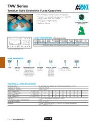
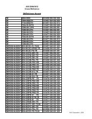
TECHNICAL INFORMATION - AVX
TECHNICAL INFORMATION - AVX
TECHNICAL INFORMATION - AVX

Create successful ePaper yourself
Turn your PDF publications into a flip-book with our unique Google optimized e-Paper software.
To study the effect of the plating thickness on the<br />
termination, chips with various plating thicknesses<br />
as characterized by the plating time were tested<br />
and the results are shown in Table 9. For 1812 size<br />
chips, the actual plated nickel thicknesses are<br />
shown in brackets. The results clearly show that at<br />
Ni thicknesses above 4.8m failures in the solder<br />
dip test increase and these may be attributed to<br />
either stresses due to the differential thermal<br />
expansions of nickel and the chip or to residual<br />
stresses. This phenomenon is not clearly understood<br />
at this time.<br />
TABLE 9<br />
THERMAL SHOCK STUDIES VS. BARRIER LAYER THICKNESS<br />
FOR CERAMIC D<br />
PLATING TIME (MIN.)<br />
7.5 15 30 60 120<br />
CHIP DESIGN OVERALL SOLDER DIP TEST RESULTS AT 260°C<br />
STYLE (ACTIVES/ CHIP (500°F), NO PREHEAT (NUMBER OF<br />
TOTAL) THICKNESS UNITS WITH VISUAL CRACKS TO<br />
IN MILS TOTAL PARTS STUDIED)<br />
(IN MM)<br />
1206 24/43 44 (1.12) 1/50 0/50 0/50 0/50 2/50<br />
1210 32/49 61 (1.55) 0/50 3/50 2/50 5/50 5/50<br />
1812 32/39 40 (1.02) 1/50 1/50 0/50 5/50 5/50<br />
80* 160* 190* 340* 725*<br />
(2.03) (4.13) (4.80) (8.70) (18.41)<br />
*ACTUAL NI BARRIER LAYER THICKNESS IN MICROINCHES (MICRONS)<br />
F. Role of Flaws<br />
In Table 3, parts made with ceramic E and F<br />
with high number of active layers were found to<br />
show higher number of visual cracks after the<br />
solder dip test and these are attributed to numerous<br />
physical flaws in these parts. To investigate the<br />
effect of physical flaws, chips made with ceramic G<br />
were tested. In this case, parts were processed<br />
through various sintering conditions for a completely<br />
different series of evaluations; the corresponding<br />
flaws generated are listed in Table 10.<br />
TABLE 10<br />
THERMAL SHOCK BEHAVIOR AS AFFECTED BY<br />
PHYSICAL FLAWS OF CERAMIC G<br />
ALL UNITS WITH PD/AG TERMINATIONS<br />
SOLDER DIP TEST RESULTS<br />
AT 425°C, NO PREHEAT<br />
TYPES OF FLAW<br />
(NUMBER OF UNITS WITH<br />
GROUP # (% OF UNITS WITH FLAWS) VISUAL CRACKS AS %)<br />
External External External<br />
Delaminations Cracks Delaminations<br />
1 71 2 100 100<br />
2 44 - 85 95<br />
3 84 - 82 90<br />
4 18 - 40 86<br />
5 77 - 87 86<br />
6 37 - 49 81<br />
7 20 - 42 81<br />
8 49 - 76 76<br />
9 5 15 7 76<br />
10* - - - 52<br />
11 40 - 9 48<br />
12 - - - 5<br />
*THIS GROUP HAS POROUS ELECTRODES WHICH MAY ACT AS SITES<br />
FOR CRACK INITIATION<br />
There is only a general correlation between number<br />
of flaws and the solder dip test results. These flaws<br />
act as crack initiation sites. Results of group 10<br />
were at first misleading because apparently no<br />
flaws were found; however, closer examination<br />
revealed porous electrodes which have already been<br />
shown to act as sites for crack initiation.<br />
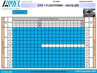
TABLE 11<br />
ROLE OF WAVE SOLDER PARAMETERS WITH WAVE TEMPERATURE<br />
OF 260°C (500°F) OF CERAMIC D<br />
ALL CHIPS ARE PLATED<br />
G. Soldering Considerations<br />
As indicated earlier, wave soldering was often<br />
used as a test vehicle to simulate the temperature<br />
and/or stress gradients in the chips studied. Two<br />
important parameters studied were the preheat<br />
temperature and the immersion rate of the part<br />
into the solder. Immersion rate was preferred over<br />
the actual temperature rise for the chips because it<br />
was impossible to read the temperature change<br />
accurately; this can be done by burying the thermocouple<br />
in the part, and the results of these experiments<br />
will be reported at a later date. The immersion<br />
rate is determined by the belt speed carrying<br />
the boards into the wave; a common rate of 1.22<br />
m/min. is used in the industry.<br />
The results of these experiments are shown in<br />
Table 11 where it is clearly seen that both the preheat<br />
and the immersion rate are critical to controlling<br />
the soldering process. Our recommendation is<br />
that the preheat temperature as measured on the<br />
board should be a maximum of 100°C below the<br />
temperature of the wave and the rate of immersion<br />
should be 1.2 m/min. Results in Table 11 show how<br />
these results may be optimized but since different<br />
ceramic materials show varying degrees of thermal<br />
shock susceptibility, the recommended conditions<br />
should be followed wherever possible.<br />
Conclusions<br />
BOARD TEST RESULTS (NUMBER<br />
OF UNITS WITH VISUAL CRACKS<br />
TO TOTAL UNITS TESTED)<br />
SOLDER CONDITIONS GROUP A GROUP B<br />
PREHEAT, IF BELT SPEED IN 1210, 01µF, 1210, 01µF,<br />
ANY (°C) FT/MIN (m/min) 25A/48T WITH 25A/35T, NO<br />
BRIDGE, 45 MILS BRIDGE, 33 MILS<br />
THICK<br />
THICK<br />
NONE 4 (1.2) 9/240 3/240<br />
20 (6.1) 51/240 6/240<br />
NONE 4 (1.2) 8/240 1/240<br />
20 (6.1) 41/240 2/240<br />
NONE 4 (1.2) 0/240 0/240<br />
10 (3.0) 15/240 1/240<br />
20 (6.1) 26/240 2/240<br />
1. Chips made from NP0 dielectric materials show<br />
excellent thermal shock behavior in surface mount<br />
applications.<br />
2. Chips made with 2-12 active layers from X7R<br />
dielectrics with bismuth containing additives may<br />
exhibit thermal shock failures if the electrodes are<br />
porous. This problem may be minimized with denser<br />
electrodes and with bridge designs.<br />
3. Bridge designs can dramatically improve thermal<br />
shock behavior exhibited by chips made with X7R<br />
dielectrics.<br />
4. Thickness of the chip plays a very important role<br />
in the overall chip design and visual cracks can be<br />
dramatically reduced with the decrease in overall<br />
chip thickness.