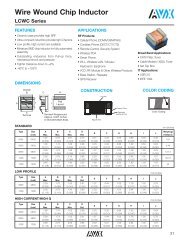
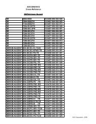
TECHNICAL INFORMATION - AVX
TECHNICAL INFORMATION - AVX
TECHNICAL INFORMATION - AVX

You also want an ePaper? Increase the reach of your titles
YUMPU automatically turns print PDFs into web optimized ePapers that Google loves.
TABLE 6<br />
EFFECT OF THICKNESS ON THERMAL SHOCK OF<br />
CERAMIC D PLATED CHIPS<br />
OVERALL CHIP THICKNESS IN MILS (mm)<br />
15 20 25 30 40 60<br />
(0.38) (0.51) (0.64) (0.76) (1.01) (1.52)<br />
CHIP STYLE SOLDER DIP TEST RESULTS AT 260°C<br />
(500°F), NO PREHEAT<br />
1206 0 0 0 0 2 3<br />
1210 0 0 0 1 2 24<br />
1812 0 0 0 2 11 41<br />
The solder dip test results, shown in Table 6, once<br />
again confirm that as the thicknesses increase the<br />
number of visual cracks increase. It should be further<br />
noted that, in general for thick parts at a constant<br />
chip thickness, as the part size increases the visual<br />
cracks increase and this is not surprising because<br />
larger geometries have larger stresses resulting<br />
from thermal mismatch between ceramic and electrode<br />
layers for the same temperature change.<br />
This information is being utilized to make optimum<br />
geometries for similar valued parts by <strong>AVX</strong>.<br />
D. Effect of Dielectric Thickness<br />
Chips were prepared with constant overall chip<br />
and cover layer thicknesses and the ceramic dielectric<br />
layer thickness was varied from 25 to<br />
229m. These results, shown in Table 7, demonstrate<br />
that the effective thermal conductivity of the<br />
composite increases as the dielectric thickness<br />
decreases which in turn decreases the temperature<br />
and stress gradients and the corresponding number<br />
of visual cracks. This experiment further supports<br />
the use of the bridge design for low active parts as a<br />
viable alternative.<br />
TABLE 7<br />
THERMAL SHOCK FAILURES AS A FUNCTION<br />
OF DIELECTRIC THICKNESS<br />
CERAMIC D, 1210 CHIPS WITH 40 MIL (1.02mm) OVERALL THICKNESS,<br />
TERMINATED AND SOLDER PLATED<br />
DIELECTRIC SOLDER DIP TEST RESULTS AT 260°C (500°F),<br />
THICKNESS NO PREHEAT<br />
IN MILS<br />
(NUMBER OF UNITS WITH VISUAL CRACKS<br />
(m)<br />
IN PERCENT)<br />
1.0 (25) 2<br />
2.0 (51) 17<br />
3.0 (76) 18<br />
4.0 (101) 16<br />
5.0 (127) 19<br />
9.0 (229) 49<br />
E. Effect of Termination<br />
As indicated earlier, termination materials play a<br />
very important role in the thermal shock behavior<br />
of MLCs. Chips made with Pd/Ag termination<br />
materials and with Ag termination which is subsequently<br />
plated with nickel and solder, and then subjected<br />
to the solder dip test show dramatic differences.<br />
An example of this behavior is shown in Table 8<br />
where 1210 size 0.1F chips made with ceramic D<br />
show no visual cracks with Pd/Ag terminations but<br />
the same parts with Ag termination which is plated<br />
with about 2.0m of nickel and 4.0m of solder<br />
show cracks in practically 100% of the parts.<br />
TABLE 8<br />
ROLE OF TERMINATION IN THERMAL SHOCK STUDIES<br />
1210 CHIPS 0.1 F CERAMIC C, 61 MILS (1.55mm) OVERALL THICKNESS<br />
Pd/Ag Ag termination Ni Barrier Ni Barrier Ni Barrier<br />
Termination with Ni Barrier parts, no parts heat parts heat<br />
and solder solder treated to treated at<br />
plated 160°C for 400°C for<br />
1 hr. 1 hr.<br />
Solder dip<br />
test results<br />
at 260°C, 0/200 199/200 100/100 70/100 0/100<br />
no preheat<br />
(number of<br />
units with<br />
visual cracks<br />
to total parts<br />
tested)<br />
These observations may be explained by the following<br />
analysis.<br />
Thermal conductivity data for Pd/Ag alloys or<br />
termination materials is not available but some<br />
estimates can be generated. Pd and Ag have<br />
thermal conductivity values of about 84 and 428<br />
Wm -1 °K - 1 respectively. 10 Typical Pd/Ag alloys are<br />
therefore expected to have values of around 200<br />
Wm -1 °K - 1 . However, most termination materials<br />
have glass frits added to improve adhesion of these<br />
materials to the MLC. Without going into the<br />
details of proprietary glass frit materials used for<br />
terminations, and utilizing average values of thermal<br />
conductivity for glasses of about 0.84 Wm -1 °K - 1<br />
along with the assumption that these glass frits<br />
form a grain boundary phase or are at the ceramictermination<br />
interface, the effective thermal conductivity<br />
can be calculated 11 to be somewhere between<br />
10 to 25 Wm -1 °K - 1 . No provision has been made for<br />
a small amount of porosity which may exist in the<br />
termination as the thermal conductivity of pores 11<br />
is around 0.02 Wm -1 °K - 1 and these values are<br />
expected to be lowered further to about 6-20<br />
Wm -1 °K - 1 . In contrast the nickel barrier is dense<br />
and nickel has a thermal conductivity of about 84<br />
Wm -1 °K - 1 which is about an order of magnitude<br />
higher. Aside from the differences in the thermal<br />
conductivities, it was observed during the solder<br />
dipping experiments that (even though both the<br />
Pd/Ag and plated barrier layer terminations wet<br />
well), the plated terminations wet much faster<br />
compared to the Pd/Ag terminated chips. This in<br />
turn implies that the surface heat transfer coefficient<br />
for the plated terminations is significantly<br />
higher compared to that for Pd/Ag parts. This<br />
nickel layer therefore transfers the heat at the<br />
termination rapidly resulting in larger stress gradients<br />
compared to parts with Pd/Ag termination<br />
only and these stress gradients result in 100% visual<br />
cracks in the solder dip test. To further illustrate<br />
the validity of this hypothesis, chips with a nickel<br />
barrier but no protective solder coating (customarily<br />
used) were oxidized at 160° and at 400°C respectively<br />
for 1 hour; solder dip test results are shown<br />
in Table 8. The results show a dramatic drop in the<br />
number of visual cracks after the solder dip test<br />
and this is attributed to an order of magnitude<br />
lower thermal conductivity of nickel oxide and to a<br />
significantly lower surface heat transfer coefficient<br />
of an oxide film. This demonstrates the importance<br />
of the role of the termination itself. The termination<br />
geometry has also been found to be a very important<br />
parameter which in turn controls the surface<br />
heat transfer coefficient and the subsequent visual<br />
cracks due to stress gradients. These aspects are<br />
utilized to control the thermal shock behavior of<br />
chips and will be discussed in the next paper. 6