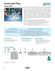
TECHNICAL INFORMATION - AVX
TECHNICAL INFORMATION - AVX
TECHNICAL INFORMATION - AVX

You also want an ePaper? Increase the reach of your titles
YUMPU automatically turns print PDFs into web optimized ePapers that Google loves.
Now that the thermal stress has been identified,<br />
its effect on crack initiation and crack propagation<br />
should be recognized. Both these processes are<br />
important for the thermal stress or thermal shock<br />
resistance of ceramic materials.<br />
1. Crack Initiation<br />
The effect of thermal stresses on different<br />
materials 3,5 depends not only on stress level,<br />
stress distribution and stress duration but also<br />
on material characteristics such as ductility,<br />
homogeneity, porosity and pre-existing flaws.<br />
Because of so many characteristics involved in<br />
the thermal stress evaluations, it is impossible to<br />
define a single thermal stress resistance factor<br />
which is satisfactory for various situations.<br />
Most electronic ceramic materials behave like<br />
ideal elastic materials which fracture when the<br />
surface stress reaches a particular level. For<br />
conditions mentioned above the thermal stress<br />
resistance factor R’ is defined in Equation 3:<br />
R’ = k f (1-) (3)<br />
E<br />
where f is the fracture stress. This equation<br />
suggests that high fracture stress, low modulus<br />
of elasticity and low thermal expansion coefficient<br />
indicate a good resistance to thermal stress<br />
failure. Once again by considering the failure<br />
criterion of fracture occurring when the thermal<br />
stress reaches the fracture stress, it is possible to<br />
estimate the maximum temperature difference<br />
which a sample can withstand and this temperature<br />
difference is directly proportional to R’ and<br />
inversely proportional to half sample thickness t<br />
and to the surface heat transfer coefficient h.<br />
The above discussion is predicated on the<br />
assumption that failure occurs when the thermal<br />
stress reaches the fracture stress. It should,<br />
however, be noted that this condition is for the<br />
nucleation or initiation of cracks only. These<br />
stresses may be initiated at a surface but may be<br />
stopped by a pore, a heterogeneity or a grain<br />
boundary. These features will be qualitatively<br />
studied in the experimental section of this paper<br />
where various dielectric materials subjected to<br />
similar thermal stresses behave quite differently.<br />
2. Crack Propagation<br />
The conditions which govern the propagation<br />
of cracks rather than the nucleation are<br />
related 8,9 to the elastic energy stored at the<br />
moment of fracture. There are two thermal<br />
shock resistance parameters 8,9 which are<br />
involved in the avoidance of catastrophic crack<br />
propagation and they show a direct proportionality<br />
to the elastic modulus E, to the surface fracture<br />
energy G and inverse dependence to f2 .<br />
Thus the favorable material characteristics for<br />
crack propagation are high modulus and high<br />
surface fracture energy and low fracture<br />
strengths, in direct contrast to conditions<br />
appropriate for avoiding the initiation of cracks.<br />
In most electronic ceramic materials conditions<br />
for avoiding crack initiation are emphasized<br />
because micro-cracks may have a deleterious<br />
effect on other properties like the electrical conductivity.<br />
This is in strong contrast to, for example,<br />
porous refractory ceramic materials where<br />
large stress gradients initiate many surface<br />
cracks which are stopped primarily by pores,<br />
grain boundaries or metal layers. These stress<br />
relief sites are therefore important for high<br />
temperature stress corrosion resistance.<br />
C. Critical Fracture Toughness<br />
Critical stresses which the ceramic materials can<br />
withstand can be determined by fracture mechanics<br />
analysis of micro-indentations based on propagation<br />
of mutually perpendicular penny-like<br />
median/radial cracks. When an indentation is put<br />
on the sample using the Vicker’s indenter, the net<br />
driving force in the crack system is a result of two<br />
superimposed components (an elastic component<br />
and a residual component) which are compressive<br />
and tensile respectively. The residual component<br />
drives the crack to its final size when the indenter<br />
is removed and the restraining elastic component<br />
results in a well-defined crack which can be measured<br />
under an optical microscope. This technique<br />
provides a means to determine critical fracture<br />
toughness,<br />
E 1/2 P<br />
(4)<br />
K1 C<br />
0.013<br />
( H ) ( Co<br />
3/2)<br />
where H is the Vicker’s hardness, P is the applied<br />
load and C o is the equilibrium crack length in an<br />
isotropic material measured soon after the indentation.<br />
The corresponding critical stress at which a<br />
crack is initiated is:<br />
C = K1 C<br />
/y C o (5)<br />
where y = 2 / π<br />
The critical stress may be anisotropic in a MLC<br />
because of residual stresses which can be determined<br />
by studying the deviation and anisotropy of<br />
the measured crack lengths. In the study of slow<br />
crack growth, the underlying assumption is that<br />
these cracks will propagate when the stress intensity<br />
in the crack tip reaches the value corresponding<br />
to K1 C<br />
. An exponent in describing the crack<br />
velocity related to the fracture toughness can be<br />
defined 3 and this allows comparison of different<br />
dielectric materials. These results will be discussed<br />
in a later paper .6<br />
II. Experimental Procedure<br />
In an effort to understand the various sources of<br />
thermal stresses and corresponding thermal stress<br />
resistance characteristics, various experiments were<br />
carried out and these are outlined below:<br />
A. Ceramic Formulations<br />
Since different materials show varying susceptibility<br />
to similar thermal shock experiments,<br />
chips were fabricated using standard capacitor<br />
manufacturing techniques 1 with various dielectric<br />
compositions classified by EIA temperature characteristics<br />
referred to as NP0, X7R and Z5U<br />
ceramics. Even within the same temperature<br />
characteristic such as an X7R there are various<br />
ceramics used and the differences are minor additives<br />
referred to as fluxes which change the sintering<br />
temperatures of these materials. Various<br />
materials used for experiments are listed in Table