- Page 1 and 2: Programmable Logic Design Quick Sta
- Page 3 and 4: ABSTRACT Whether you design with di
- Page 5 and 6: NAVIGATING THIS BOOK C HAPTER 5: IM
- Page 7 and 8: TABLE OF CONTENTS Virtex FPGAs.....
- Page 9 and 10: TABLE OF CONTENTS MicroBlaze and Pi
- Page 11 and 12: Chapter 7: Design Reference Bank TA
- Page 13 and 14: C HAPTER 1 Introduction The History
- Page 15 and 16: INTRODUCTION Other architectures fo
- Page 17 and 18: INTRODUCTION vides an instant hardw
- Page 19 and 20: INTRODUCTION FIGURE 1-4: FPGA ARCHI
- Page 21 and 22: INTRODUCTION By using Xilinx CoolRu
- Page 23 and 24: INTRODUCTION FIGURE 1-8: DESIGN SPE
- Page 25 and 26: INTRODUCTION For the HDL specificat
- Page 27 and 28: INTRODUCTION Even if you decide to
- Page 29 and 30: INTRODUCTION original I/O pin place
- Page 31 and 32: INTRODUCTION FIGURE 1-11: DEVICE IM
- Page 33 and 34: C HAPTER 2 Xilinx Solutions Introdu
- Page 35 and 36: XILINX SOLUTIONS The Platform FPGA
- Page 37 and 38: . XILINX SOLUTIONS FIGURE 2-2: PLAT
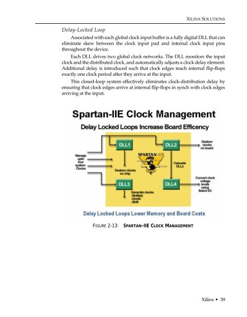
- Page 39 and 40: XILINX SOLUTIONS FIGURE 2-4: SPARTA
- Page 41 and 42: XILINX SOLUTIONS • Full- and half
- Page 43 and 44: TABLE 2-3: SPARTAN-3 FEATURES AND B
- Page 45 and 46: XILINX SOLUTIONS FIGURE 2-6: SPARTA
- Page 47 and 48: XILINX SOLUTIONS FIGURE 2-8: SPARTA
- Page 49: XILINX SOLUTIONS FIGURE 2-10: SPART
- Page 53 and 54: XILINX SOLUTIONS FIGURE 2-15: SPART
- Page 55 and 56: XILINX SOLUTIONS Low Power - Is you
- Page 57 and 58: XILINX SOLUTIONS XC9500XL family is
- Page 59 and 60: XILINX SOLUTIONS TABLE 2-5: XC9500X
- Page 61 and 62: XILINX SOLUTIONS caded chain of pur
- Page 63 and 64: XILINX SOLUTIONS FIGURE 2-22: COOLR
- Page 65 and 66: I/O Cell XILINX SOLUTIONS The outpu
- Page 67 and 68: TABLE 2-6: VFM (Variable Function M
- Page 69 and 70: XILINX SOLUTIONS Figure 2-27 also d
- Page 71 and 72: XILINX SOLUTIONS At the high level,
- Page 73 and 74: XILINX SOLUTIONS FIGURE 2-30: COOLR
- Page 75 and 76: XILINX SOLUTIONS The larger parts (
- Page 77 and 78: XILINX SOLUTIONS Note that a synchr
- Page 79 and 80: XILINX SOLUTIONS These security bit
- Page 81 and 82: XILINX SOLUTIONS COOLRUNNER REFEREN
- Page 83 and 84: . XILINX SOLUTIONS FIGURE 2-42: LOG
- Page 85 and 86: XILINX SOLUTIONS To address the nee
- Page 87 and 88: XILINX SOLUTIONS This rich mixture
- Page 89 and 90: Dynamic Verification XILINX SOLUTIO
- Page 91 and 92: XILINX SOLUTIONS Xilinx IP Cores Th
- Page 93 and 94: XILINX SOLUTIONS • Test and Measu
- Page 95 and 96: XILINX SOLUTIONS be fixed, upgraded
- Page 97 and 98: XILINX SOLUTIONS TABLE 2-10: XILINX
- Page 99 and 100: XILINX SOLUTIONS CONNECTIVITY CENTR
- Page 101 and 102:
XILINX SOLUTIONS design • Broad a
- Page 103 and 104:
Xilinx Student Edition Frequently A
- Page 105 and 106:
C HAPTER 3 WebPACK ISE Design Softw
- Page 107 and 108:
WEBPACK ISE DESIGN SOFTWARE 4. Gene
- Page 109 and 110:
WEBPACK ISE DESIGN SOFTWARE WEBPACK
- Page 111 and 112:
Summary PROJECTS WEBPACK ISE DESIGN
- Page 113 and 114:
C HAPTER 4 WebPACK ISE Design Entry
- Page 115 and 116:
WEBPACK ISE DESIGN ENTRY FIGURE 4-2
- Page 117 and 118:
WEBPACK ISE DESIGN ENTRY Notice tha
- Page 119 and 120:
WEBPACK ISE DESIGN ENTRY As you hav
- Page 121 and 122:
WEBPACK ISE DESIGN ENTRY The area s
- Page 123 and 124:
WEBPACK ISE DESIGN ENTRY Click OK t
- Page 125 and 126:
WEBPACK ISE DESIGN ENTRY Maximize t
- Page 127 and 128:
WEBPACK ISE DESIGN ENTRY Open the S
- Page 129 and 130:
WEBPACK ISE DESIGN ENTRY Set RD to
- Page 131 and 132:
WEBPACK ISE DESIGN ENTRY In the edi
- Page 133 and 134:
Click on the Generate HDL button on
- Page 135 and 136:
WEBPACK ISE DESIGN ENTRY Click on t
- Page 137 and 138:
WEBPACK ISE DESIGN ENTRY Connect th
- Page 139 and 140:
You are now ready to go to the impl
- Page 141 and 142:
WEBPACK ISE DESIGN ENTRY Move the c
- Page 143 and 144:
Your completed schematic should loo
- Page 145 and 146:
C HAPTER 5 Implementing CPLDs Intro
- Page 147 and 148:
IMPLEMENTING CPLDS The design shoul
- Page 149 and 150:
IMPLEMENTING CPLDS Notice that the
- Page 151 and 152:
DoubLe-click in the Period window o
- Page 153 and 154:
IMPLEMENTING CPLDS In the Clock to
- Page 155 and 156:
IMPLEMENTING CPLDS Click on the “
- Page 157 and 158:
IMPLEMENTING CPLDS To open the CPLD
- Page 159 and 160:
IMPLEMENTING CPLDS MXE will open, b
- Page 161 and 162:
C HAPTER 6 Implementing FPGAs Intro
- Page 163 and 164:
IMPLEMENTING FPGAS Double-click on
- Page 165 and 166:
IMPLEMENTING FPGAS The FSM encoding
- Page 167 and 168:
IMPLEMENTING FPGAS The Constraints
- Page 169 and 170:
IMPLEMENTING FPGAS Highlight the th
- Page 171 and 172:
IMPLEMENTING FPGAS Save and close t
- Page 173 and 174:
IMPLEMENTING FPGAS Programming Righ
- Page 175 and 176:
C HAPTER 7 Design Reference Bank In
- Page 177 and 178:
DESIGN REFERENCE BANK A high-powere
- Page 179 and 180:
DESIGN REFERENCE BANK USING A MICRO
- Page 181 and 182:
DESIGN REFERENCE BANK port ( clk :
- Page 183 and 184:
DESIGN REFERENCE BANK vated, it wil
- Page 185 and 186:
DESIGN REFERENCE BANK Figure 7-7 sh
- Page 187 and 188:
DESIGN REFERENCE BANK Full-function
- Page 189 and 190:
DESIGN REFERENCE BANK TABLE 7-1: DO
- Page 191 and 192:
DESIGN REFERENCE BANK TABLE 7-1: DO
- Page 193 and 194:
ACRONYMS ABEL ADC AIM ANSI ASIC ASS
- Page 195 and 196:
ACRONYMS LVDS Low Voltage Different
- Page 198 and 199:
PROGRAMMABLE LOGIC DESIGN -- QUICK
- Page 200 and 201:
PROGRAMMABLE LOGIC DESIGN -- QUICK
- Page 202 and 203:
PROGRAMMABLE LOGIC DESIGN -- QUICK
- Page 204 and 205:
PROGRAMMABLE LOGIC DESIGN -- QUICK
- Page 206:
PROGRAMMABLE LOGIC DESIGN -- QUICK