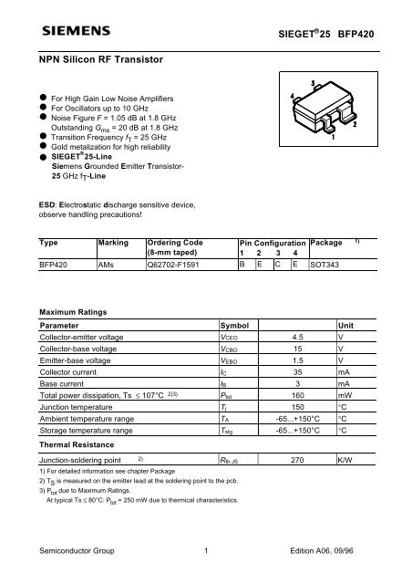
NPN Silicon RF Transistor Bfp420
NPN Silicon RF Transistor Bfp420
NPN Silicon RF Transistor Bfp420

Create successful ePaper yourself
Turn your PDF publications into a flip-book with our unique Google optimized e-Paper software.
SIEGET ® 25 BFP420<br />
<strong>NPN</strong> <strong>Silicon</strong> <strong>RF</strong> <strong>Transistor</strong><br />
For High Gain Low Noise Amplifiers<br />
For Oscillators up to 10 GHz<br />
Noise Figure F = 1.05 dB at 1.8 GHz<br />
Outstanding G ms = 20 dB at 1.8 GHz<br />
Transition Frequency f T = 25 GHz<br />
Gold metalization for high reliability<br />
SIEGET ® 25-Line<br />
Siemens Grounded Emitter <strong>Transistor</strong>-<br />
25 GHz f T -Line<br />
ESD: Electrostatic discharge sensitive device,<br />
observe handling precautions!<br />
Type Marking Ordering Code<br />
(8-mm taped)<br />
Pin Configuration<br />
1 2 3 4<br />
Package 1)<br />
BFP420 AMs Q62702-F1591 B E C E SOT343<br />
Maximum Ratings<br />
Parameter Symbol Unit<br />
Collector-emitter voltage VCEO 4.5 V<br />
Collector-base voltage VCBO 15 V<br />
Emitter-base voltage VEBO 1.5 V<br />
Collector current IC 35 mA<br />
Base current IB 3 mA<br />
Total power dissipation, Ts ≤ 107°C 2)3) Ptot 160 mW<br />
Junction temperature Tj 150 °C<br />
Ambient temperature range TA -65...+150°C °C<br />
Storage temperature range Tstg -65...+150°C °C<br />
Thermal Resistance<br />
Junction-soldering point 2) Rth JS 270 K/W<br />
1) For detailed information see chapter Package<br />
2) T S is measured on the emitter lead at the soldering point to the pcb.<br />
3) P tot due to Maximum Ratings.<br />
At typical Ts ≤ 80°C: P tot = 250 mW due to thermical characteristics.<br />
Semiconductor Group 1 Edition A06, 09/96
SIEGET ® 25 BFP420<br />
Electrical Characteristics<br />
at TA = 25 °C, unless otherwise specified.<br />
Parameter Symbol Value Unit<br />
min. typ. max.<br />
DC Characteristics<br />
Collector-emitter breakdown voltage<br />
IC = 1 mA<br />
Collector-cutoff current<br />
VCB = 5 V, IE = 0<br />
Emitter base cuttoff current<br />
VEB = 1.5 V, IC = 0<br />
DC current gain<br />
IC = 20 mA, VCE = 4 V<br />
V(BR)CEO 4.5 5 6.5 V<br />
ICBO - - 200 nA<br />
IEBO - - 35 µA<br />
hFE 50 80 150<br />
AC Characteristics<br />
Transition frequency<br />
IC = 30 mA, VCE = 3 V, f = 2 GHz<br />
Collector-base capacitance<br />
VCB = 2 V, VBE = vbe = 0, f = 1 MHz<br />
Collector-emitter capacitance<br />
VCE = 2 V, VBE = vbe = 0, f = 1 MHz<br />
Emitter-base capacitance<br />
VEB = 0.5 V, VCB = vcb = 0, f = 1 MHz<br />
Noise figure<br />
IC = 5 mA, VCE = 2 V, f = 1.8 GHz, ZS = ZSopt<br />
Power gain<br />
IC = 20 mA, VCE = 2 V, f = 1.8 GHz,<br />
fT 20 25 - GHz<br />
Ccb - 0.15 0.24 pF<br />
Cce - 0.41 - pF<br />
Ceb - 0.55 - pF<br />
F - 1.05 1.4 dB<br />
G ms<br />
1) - 20 - dB<br />
ZS =ZSopt , ZL = ZLopt<br />
Insertion power gain<br />
|S 21 | 2 14 17 - dB<br />
IC = 20 mA, VCE = 2 V, f = 1.8 GHz, ZS = ZL = 50Ω<br />
Third order intercept point at output<br />
IP 3 - 22 - dBm<br />
ZS = ZSopt, Z L = Z Lopt<br />
IC = 20 mA, VCE = 2 V, f = 1.8 GHz,<br />
1dB Compression point<br />
P -1dB - 12 - dBm<br />
ZS = ZSopt, Z L = Z Lopt<br />
IC = 20 mA, VCE = 2 V, f = 1.8 GHz,<br />
S<br />
1) Gms = 21<br />
S12<br />
Semiconductor Group 2 Edition A06, 09/96
SIEGET ® 25 BFP420<br />
Total Power Dissipation<br />
Permissible Pulse Power Dissipation<br />
versus Soldering Point Temperature versus On-Time (V CE0max = 4.5 V)<br />
Ptot<br />
600<br />
mW<br />
500<br />
400<br />
Ptot_max<br />
Ptot_DC<br />
300<br />
200<br />
according maximum ratings<br />
100<br />
50 100 °C<br />
150<br />
Ts<br />
tp<br />
Transition Frequency<br />
versus Collector Current<br />
f = 2 GHz<br />
Collector-base Capacitance<br />
versus Collector-base Voltage<br />
V BE = 0 V, f = 1MHz<br />
30<br />
0.3<br />
fT<br />
GHz<br />
25<br />
Vce= 3 V, 4 V<br />
1 V<br />
2 V<br />
Ccb<br />
pF<br />
0.25<br />
20<br />
0.2<br />
15<br />
0.5 V<br />
0.15<br />
10<br />
0.1<br />
5<br />
0.05<br />
10 20 mA<br />
40<br />
Ic<br />
1 2 V<br />
4<br />
Vcb<br />
Semiconductor Group 3 Edition A06, 09/96
SIEGET ® 25 BFP420<br />
Power Gain<br />
versus Frequency<br />
V CE = 2 V , I C = 20 mA<br />
Power Gain<br />
versus Collector Current<br />
V CE = 2 V<br />
60<br />
dB<br />
30<br />
dB<br />
f= 1 GHz<br />
Gma<br />
Gms<br />
|S21|²<br />
50<br />
40<br />
Gma<br />
Gms<br />
25<br />
20<br />
2 GHz<br />
30<br />
Gms<br />
15<br />
3 GHz<br />
4 GHz<br />
5 GHz<br />
20<br />
|S21|²<br />
Gma<br />
10<br />
6 GHz<br />
10<br />
5<br />
0.1 1 GHz 10<br />
Power Gain<br />
versus Collector Voltage<br />
I C = 20 mA<br />
f<br />
10 20 mA<br />
40<br />
Ic<br />
30<br />
Gma<br />
Gms<br />
dB<br />
25<br />
20<br />
15<br />
10<br />
f= 1 GHz<br />
2 GHz<br />
3 GHz<br />
4 GHz<br />
5 GHz<br />
6 GHz<br />
5<br />
1<br />
2<br />
3<br />
V<br />
4<br />
Vce<br />
Semiconductor Group 4 Edition A06, 09/96
SIEGET ® 25 BFP420<br />
Noise Figure<br />
versus Collector Current<br />
VCE = 2 V, ZS = ZSopt<br />
Noise Figure<br />
versus Collector Current<br />
VCE = 2 V, f = 1.8 GHz<br />
F<br />
3<br />
dB<br />
2.5<br />
6.0 GHz<br />
5.0 GHz<br />
4.0 GHz<br />
F<br />
3<br />
dB<br />
2.5<br />
3.0 GHz<br />
2<br />
2.4 GHz<br />
1.8 GHz<br />
2<br />
Zs=50 Ohms<br />
1.5<br />
1.5<br />
0.9 GHz<br />
1<br />
1<br />
Zsopt<br />
0.5<br />
0.5<br />
10 20 mA<br />
40<br />
Ic<br />
10 20 mA<br />
40<br />
Ic<br />
Noise Figure versus Frequency<br />
VCE = 2 V, I C = 5 mA / 20 mA,<br />
ZS = ZSopt<br />
Source Impedance for min.<br />
Noise Figure versus Frequency<br />
V CE = 2 V, I C = 5 mA / 20 mA<br />
F<br />
3<br />
dB<br />
2.5<br />
2<br />
1.5<br />
20 mA<br />
+j10<br />
0<br />
+j25<br />
10<br />
+j50<br />
2.4 GHz<br />
3 GHz<br />
4 GHz<br />
25<br />
50<br />
1.8 GHz<br />
0.9 GHz<br />
5 mA<br />
100<br />
+j100<br />
1<br />
5 mA<br />
-j10<br />
5 GHz<br />
6 GHz<br />
20 mA<br />
0.5<br />
-j25<br />
-j100<br />
0.1 1 GHz 10<br />
f<br />
-j50<br />
Semiconductor Group 5 Edition A06, 09/96
SIEGET ® 25 BFP420<br />
Common Emitter S-Parameters<br />
ƒ S11 S 21 S 12 S 22<br />
GHz MAG ANG MAG ANG MAG ANG MAG ANG<br />
V CE = 2 V, I C = 20 mA<br />
0.01 0.452 -2.3 37.62 178.3 0.0011 94.4 0.956 -0.6<br />
0.1 0.447 -25.1 36.30 164.7 0.0068 82.5 0.941 -12.4<br />
0.5 0.386 -101.1 23.41 121.0 0.0262 61.7 0.632 -47.2<br />
1.0 0.378 -146.2 13.99 96.0 0.0395 57.8 0.395 -63.9<br />
2.0 0.405 173.5 7.18 70.8 0.0664 54.0 0.222 -87.3<br />
3.0 0.446 149.4 4.77 52.6 0.0949 47.1 0.133 -111.3<br />
4.0 0.501 130.0 3.52 36.8 0.1206 38.5 0.133 -158.5<br />
6.0 0.599 104.8 2.27 8.2 0.1646 18.9 0.196 142.0<br />
8.0 0.700 78.5 1.51 -20.8 0.1800 -2.4 0.289 99.3<br />
9.0 0.758 67.6 1.25 -34.4 0.1820 -13.0 0.379 84.1<br />
10.0 0.800 62.0 1.04 -43.5 0.1800 -19.3 0.465 76.6<br />
V CE = 2 V, I C = 5 mA<br />
0.01 0.790 -1.0 15.14 179.2 0.0012 83.4 0.988 -0.7<br />
0.1 0.786 -11.6 14.98 171.8 0.0092 84.1 0.982 -6.5<br />
0.5 0.702 -55.7 12.86 140.1 0.0398 62.8 0.857 -29.8<br />
1.0 0.589 -99.1 9.63 112.6 0.0603 46.5 0.647 -48.6<br />
2.0 0.507 -156.0 5.60 79.4 0.0798 34.6 0.401 -70.3<br />
3.0 0.511 168.5 3.84 57.1 0.0957 29.8 0.267 -84.2<br />
4.0 0.549 142.0 2.87 38.5 0.1121 25.1 0.207 -110.5<br />
5.0 0.604 123.9 2.26 22.1 0.1285 19.4 0.150 -137.3<br />
6.0 0.633 110.0 1.86 6.7 0.1442 13.1 0.173 -169.8<br />
Common Emitter Noise Parameters<br />
ƒ Fmin 1) G a 1) Γ opt R N r n F 50Ω 2) |S 21 | 2 2)<br />
GHz dB dB MAG ANG Ω - dB dB<br />
V CE = 2 V, I C = 5 mA<br />
0.9 0.90 20.5 0.28 41.0 8.7 0.17 1.02 20.3<br />
1.8 1.05 15.2 0.20 82.0 6.7 0.13 1.11 15.8<br />
2.4 1.25 13.0 0.20 124.0 5.5 0.11 1.32 13.5<br />
3.0 1.38 12.1 0.22 -175.0 5.0 0.10 1.48 11.6<br />
4.0 1.55 10.3 0.33 -157.0 5.5 0.11 1.83 9.1<br />
5.0 1.75 8.6 0.45 -142.0 5.0 0.10 2.20 7.0<br />
6.0 2.20 6.4 0.53 -123.0 15.0 0.30 3.30 5.3<br />
1) Input matched for minimum noise figure, output for maximum gain 2) ZS=ZL=50Ω<br />
For more and detailed S- and Noise-parameters please contact your local Siemens distributor or sales office to<br />
obtain a SIEMENS Application Notes CD-ROM or see Internet:<br />
http://www.siemens.de/Semiconductor/products/35/357.htm<br />
Semiconductor Group 6 Edition A06, 09/96
SIEGET ® 25 BFP420<br />
SPICE Parameters:<br />
<strong>Transistor</strong> Chip Data T502 (Berkeley-SPICE 2G.6 Syntax):<br />
IS = 0.20045 fA BF = 72.534 - NF = 1.2432 -<br />
VAF = 28.383 V IKF = 0.48731 A ISE = 19.049 fA<br />
NE = 2.0518 - BR = 7.8287 - NR = 1.3325 -<br />
VAR = 19.705 V IKR = 0.69141 A ISC = 0.019237 fA<br />
NC = 1.1724 - RB = 3.4849 OHM IRB = 0.72983 mA<br />
RBM = 8.5757 OHM RE = 0.31111 OHM RC = 0.10105 OHM<br />
CJE = 1.8063 fF VJE = 0.8051 V MJE = 0.46576 -<br />
TF = 6.7661 ps XTF = 0.42199 - VTF = 0.23794 V<br />
ITF = 1.0 mA PTF = 0 deg CJC = 234.53 fF<br />
VJC = 0.81969 V MJC = 0.30232 - XCJC = 0.3 -<br />
TR = 2.3249 ns CJS = 0 fF VJS = 0.75 V<br />
MJS = 0 - XTB = 0 - EG = 1.11 eV<br />
XTI = 3.0 - FC = 0.73234 - Tnom = 300 K<br />
C'-E'- Diode Data (Berkeley-SPICE 2G.6 Syntax):<br />
IS = 3.5 fA N = 1.02 - RS = 10 Ω<br />
All parameters are ready to use, no scaling is necessary.<br />
Package Equivalent Circuit:<br />
CCB<br />
SOT343-3:<br />
B<br />
LBO<br />
LBI<br />
CBE<br />
B'<br />
transistor<br />
chip<br />
E'<br />
LEI<br />
C'<br />
LCI<br />
C'-E'-diode<br />
CCE<br />
LCO<br />
C<br />
LBI = 0.47 nH<br />
LBO = 0.53 nH<br />
LEI = 0.23 nH<br />
LEO = 0.05 nH<br />
LCI = 0.56 nH<br />
LCO = 0.58 nH<br />
CBE = 136 fF<br />
CCE = 134 fF<br />
CCB = 6.9 fF<br />
LEO<br />
E<br />
valid up to 6 GHz<br />
The SOT343 package has two emitter leads. To avoid high complexity of the package equivalent circuit,<br />
both leads are combined in one electrical connection.<br />
Extracted on behalf of SIEMENS Small Signal Semiconductors by:<br />
Institut für Mobil- und Satellitenfunktechnik (IMST)<br />
© 1996 SIEMENS AG<br />
For more examples and ready to use parameters please contact your local Siemens distributor or sales office to<br />
obtain a SIEMENS Application Notes CD-ROM or see Internet:<br />
http://www.siemens.de/Semiconductor/products/35/357.htm<br />
Semiconductor Group 7 Edition A06, 09/96
SIEGET ® 25 BFP420<br />
For non-linear simulation:<br />
• Use transistor chip parameters in Berkeley SPICE 2G.6 syntax for all simulators.<br />
• If you need simulation of the reverse characteristics, add the diode with the C'-E'-diode data between<br />
collector and emitter.<br />
• Simulation of the package is not necessary for frequencies < 100 MHz.<br />
For higher frequencies add the wiring of the package equivalent circuit around the non-linear transistor<br />
and diode model.<br />
Note:<br />
- This transistor is constructed in a common emitter configuration. This feature causes an additional,<br />
reverse biased diode between emitter and collector, which does not effect normal operation.<br />
<strong>Transistor</strong> Schematic Diagram<br />
The common emitter configuration shows the following advantages:<br />
• Higher gain because of lower emitter inductance.<br />
• Power is dissipated via the grounded emitter leads, because the chip is mounted on the copper<br />
emitter leadframe.<br />
Please note, that the broadest lead is the emitter lead.<br />
- The AC-Characteristics are verified by random sampling.<br />
Semiconductor Group 8 Edition A06, 09/96
SIEGET ® 25 BFP420<br />
Package<br />
Published by Siemens AG, Bereich Bauelemente, Vertrieb,<br />
Produkt-Information, Balanstraße 73, D-81541 München<br />
© Siemens AG 1994. All Rights Reserved<br />
As far as patents or other rights of third parties are<br />
concerned, liability is only assumed for components per<br />
se,not for applications,processes and circuits implemented<br />
within components or assemblies.<br />
The information describes the type of component and shall<br />
not be considered as assured characteristics.<br />
Terms of delivery and rights to change design reserved.<br />
For questions on technology, delivery and prices please contact<br />
the Offices of Semiconductor Group in Germany or the<br />
Siemens Companies and Representatives woldwide<br />
(see address list).<br />
Due to technical requirements components may contain<br />
dangerous substances. For information on the type in<br />
question please contact your nearest Siemens Office,<br />
Semiconductor Group.<br />
Siemens AG is an approved CECC manufacturer.<br />
Semiconductor Group 9 Edition A06, 09/96