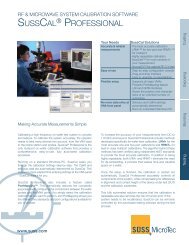
Wafer Level Reliability Testing
Wafer Level Reliability Testing
Wafer Level Reliability Testing

Create successful ePaper yourself
Turn your PDF publications into a flip-book with our unique Google optimized e-Paper software.
Flip Chip Bonders<br />
Substrate Bonders<br />
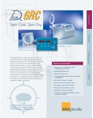
Spin Coaters<br />
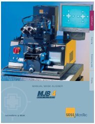
Mask Aligners<br />
<strong>Wafer</strong> <strong>Level</strong> <strong>Reliability</strong> <strong>Testing</strong><br />
Probe Systems<br />
www.suss.com
The Celadon 220 mm Probecard tile<br />
Celadon uses the inherent benefits of ceramic –<br />
high resisivity and low noise to make ideal low leakage<br />
probe cards for reliability testing. The Celadon<br />
Ceramic Tile TM which anchors the probe needles<br />
in place is mounted mounted on a rigid aluminum<br />
chassis which can be configured with several<br />
different connector housings depending on the<br />
test requirements. The large 220mm tiles used in<br />
this application are designed to provide total wafer<br />
coverage, enabling probe placement anywhere on<br />
the wafer.<br />
whole wafer. This movement has been especially<br />
designed with user comfort in mind and has the<br />
control knobs ergonomically placed on the righthand<br />
side of the prober so that one-handed use is<br />
possible. Single chip stepping is accurately undertaken<br />
with a high resolution chuck stage.<br />
The Keithley 4200 Semiconductor<br />
Characterization System<br />
The Celadon tiles and chassis have been designed<br />
to operate consistently for thousands of hours at<br />
300°C with no deterioration in electrical performance.<br />
The rigid ceramic prevents any flex or movement<br />
with empirical evidence indicating little or no observable<br />
movement in the probes during use. High<br />
current and high voltage probes are also available.<br />
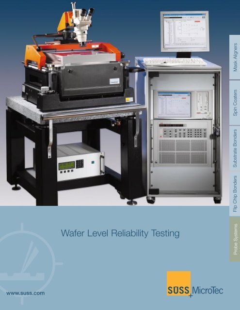
The SUSS PM8WLR ProbeShield<br />
The PM8WLR ProbeShield is a light-tight, EMI<br />
shielded probe system which has been especially<br />
designed with the demands of wafer level reliability in<br />
mind. The prober contains a thermal chuck which has<br />
a temperature range from – 60°C to + 300°C and the<br />
ProbeShield's rinsing system ensures frost-free<br />
conditions when probing at sub-zero temperatures.<br />
The Model 4200-SCS provides a total system<br />
solution for DC characterization and stress-measure/<br />
reliability testing of semiconductor devices and test<br />
structures. This advanced parameter analyzer<br />
provides intuitive and sophisticated capabilities for<br />
semiconductor device characterization. The 4200-<br />
SCS combines unprecedented measurement<br />
speed and accuracy with an embedded Windows<br />
NT- or XP based PC and the Keithley Interactive<br />
Test Environment (KITE) to provide a powerful singlebox<br />
solution.<br />
Modular and configurable, the Model 4200-SCS<br />
supports up to eight Source-Measure Units,<br />
including up to four high power SMUs with 1A/20W<br />
capability. An optional Remote PreAmp extends the<br />
resolution of any Source-Measure Unit from 100fA<br />
to 0.1fA.<br />
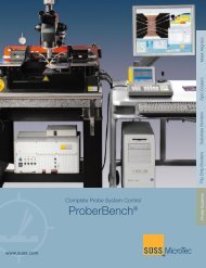
Probe Systems<br />
Because the probe card contacts all dies simultaneously,<br />
the microscope and not the chuck must<br />
move to perform correct probe to pad alignment.<br />
This PM8 has a special microscope stage which<br />
can move 200 mm in both X & Y to cover the
A Unique Multi-site, <strong>Wafer</strong> <strong>Level</strong> Solution for <strong>Reliability</strong> <strong>Testing</strong><br />
The demands of today’s technologies require<br />
precise and economical characterization. Until now,<br />
long-term testing of wafers took a great deal of both<br />
time and money as devices had to be packaged<br />
before testing. Recent innovations in thinner oxides<br />
and gate dielectrics makes packaging devices<br />
without damaging them difficult.<br />
Developed to meet the critical needs of 90 nm or<br />
smaller process technologies used by semiconductor<br />
manufacturers, the SUSS PM8WLR Probe-<br />
Shield system, in combination with Celadon probe<br />
cards and Keithley measurement equipment, provides<br />
long-term process reliability at temperatures up<br />
to 300°C.<br />
In order to prevent the loss of processed and therefore<br />
expensive wafers, it has become essential to<br />
be able to perform reliability tests on the wafer itself.<br />
The importance of this test option will grow in the<br />
near future as process technologies move towards<br />
the 90 nm range. Multi-site probing speeds up the<br />
process and enables the test engineer to obtain<br />
reasonable sample sizes. The need to measure and<br />
characterize now demands low leakage measurement<br />
equipment which can withstand temperatures<br />
up to and exceeding 300°C which accelerates<br />
failure mechanisms.<br />
The SUSS PM8WLR ProbeShield ® system has been<br />
especially developed for extremely accurate, hightemperature,<br />
multi-site <strong>Wafer</strong> <strong>Level</strong> <strong>Reliability</strong> (WLR)<br />
measurements, such as:<br />
● Electro-migration<br />
● TDDB<br />
● Hot carrier<br />
● <strong>Wafer</strong> level burn-in<br />
● Life test<br />
● Device characterization<br />
Features and Benefits<br />
• Light-tight and EMI shielded environment for<br />
ultra low-signal measurements<br />
• Rinsing system for a frost-free environment<br />
down to –60°C<br />
• Celadon’s 220 mm round probe cards provide<br />
total coverage for 150 mm & 200 mm wafers<br />
• Feed-through’s for 14 x 25 triaxial low-leakage<br />
cable harnesses: max. 350 different electrical<br />
signals<br />
• 50 x 50 mm X-Y high resolution chuck stage<br />
for one chip stepping<br />
• Extremely rigid and stable Z-chuck axis for<br />
high temperature and long time testing with<br />
high pin count probe cards<br />
• 200 x 200 mm X-Y ergonomic microscope<br />
movement with one handed operation<br />
• Ergonomic wafer load/unload via a pull-out<br />
chuck system
<strong>Wafer</strong> <strong>Level</strong> <strong>Reliability</strong><br />
<strong>Testing</strong> vs. Packaged<br />
Part <strong>Testing</strong><br />
<br />
Saving both time and money<br />
A simple application example can show the<br />
savings that can be gained from multi-site<br />
testing at wafer level. This example examines<br />
the time factor in TDDB testing<br />
Packaged Die: Time 300 hours<br />
Because a packaged part tester is noisy in<br />
itself, the engineer must wait for the leakage<br />
values to significantly increase above the<br />
machine's noise floor before he can be confident<br />
of accurate results.<br />
<strong>Wafer</strong> <strong>Level</strong> <strong>Testing</strong>: Time 12 Hours<br />
The much lower noise floor of the parametric<br />
analyzer, analytical probe station, and probe<br />
card allowed the customer to see precise<br />
leakage trends in an "over-night” test.<br />
Both packaged and wafer level tests were run at the<br />
same temperature and electrical stress levels.<br />
<br />
Microscope & mount provide necessary<br />
long working distance<br />
Customized Celadon 220 mm round<br />
high-temperature probe card<br />
<br />
Customized thermal chuck<br />
Temp. range: -60°C to + 300°C<br />
50 x 50 mm X - Y high resolution chuck<br />
stage with extremely stable Z-chuck axis<br />
SUSS ProbeShield EMC:<br />
Light-tight, frost-free probing in an EMI<br />
shielded environment<br />
200 x 200 mm X-Y one-handed microscope<br />
travel incl. fast and fine movement
Keithley 4200:<br />
Advanced Parameter Analyzer with<br />
point and click Window's ® based<br />
functionality<br />
Probe Systems<br />
Special remote adjustment and levelling<br />
tool for the Celadon Probecard
ASIA<br />
SUSS MicroTec KK (Japan)<br />
GITC 1-18-2, Hakusan, Midori-ku<br />
Yokohama, Kanagawa, Japan 226-0006<br />
Phone (+81)-45-9 31-56 00<br />
Fax (+81)-45-931-56 01<br />
EUROPE<br />
SUSS MicroTec S.A.S.<br />
131, impasse Bartheudet · BP24<br />
F-74490 Saint Jeoire · France<br />
Phone (+33)-(0) 4 50 35 83 92<br />
Fax (+33)-(0) 4 50 35 88 01<br />
JZ/DD · 04/2004<br />
SUSS MicroTec (Shanghai) Co., Ltd.<br />
580 Nanjing W. Rd · Nanzheng Building Room 606<br />
200041 Shanghai · PRC<br />
Phone (+86) 21-52 34 04 32<br />
Fax (+86) 21-52 34 04 30<br />
SUSS MicroTec (Taiwan) Co., Ltd.<br />
8F-11 · No. 81 · Shui-Lee Road<br />
Hsin-Chu · 300 · Taiwan<br />
Phone (+886)-(3)-5 16 90 98<br />
Fax (+886)-(3)-5 16 92 62<br />
SUSS MicroTec Co., Ltd.<br />
(South and Southeast Asia)<br />
3388/92-93 · 25th Floor · Sirinrat Building<br />
Rama IV Road · Klongtoey<br />
Bangkok 10110 · Thailand<br />
Phone (+66)-(0)-23 50 60 38<br />
Fax (+66)-(0)-26 33 57 28<br />
SUSS MicroTec Test Systems GmbH<br />
Süss-Strasse 1 · D-01561 Sacka/Dresden<br />
Germany<br />
Phone (+49)-(0) 35240-73-0<br />
Fax (+49)-(0) 35240-73-700<br />
NORTH AMERICA<br />
SUSS MicroTec Inc.<br />
228 Suss Drive<br />
Waterbury Center, VT 05677 · USA<br />
Phone (+1) (802) 244-5181<br />
Fax (+1) (802) 244-7853<br />
SUSS MicroTec Inc.<br />
Western Regional Sales Office<br />
8240 So. Kyrene Road Suite 101<br />
Tempe, AZ 85284-2117 · USA<br />
Phone (+1) (480) 557-9370<br />
Fax (+1) (480) 557-9371<br />
PM8WLR · DE · 04/2004 · #1 · 2000<br />
www.suss.com<br />
SUSS WLR Test Partners featured in Brochure:<br />
www.celadonsystems.com<br />
www.keithley.com