PS7341(L) - California Eastern Laboratories
PS7341(L) - California Eastern Laboratories
PS7341(L) - California Eastern Laboratories

You also want an ePaper? Increase the reach of your titles
YUMPU automatically turns print PDFs into web optimized ePapers that Google loves.
Solid State Relay<br />
OCMOS FET<br />
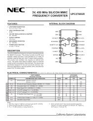
<strong>PS7341</strong>-1A,<strong>PS7341</strong>L-1A<br />
6-PIN DIP, HIGH ISOLATION VOLTAGE<br />
400 V BREAK DOWN VOLTAGE<br />
NORMALLY OPEN TYPE<br />
1-ch Optical Coupled MOS FET<br />
−NEPOC Series−<br />
DESCRIPTION<br />
The <strong>PS7341</strong>-1A and <strong>PS7341</strong>L-1A are solid state relays containing GaAs LEDs on the light emitting side (input side)<br />
and MOS FETs on the output side.<br />
They are suitable for analog signal control because of their low offset and high linearity.<br />
The <strong>PS7341</strong>L-1A has a surface mount type lead.<br />
<br />
<br />
FEATURES<br />
• High isolation voltage (BV = 3 750 Vr.m.s.)<br />
• 1 channel type (1 a output)<br />
• Low LED Operating Current (IF = 2 mA)<br />
• Designed for AC/DC switching line changer<br />
• Small package (6-pin DIP)<br />
• Low offset voltage<br />
• Ordering number of taping product : <strong>PS7341</strong>L-1A-E3, E4: 1 000 pcs/reel<br />
• Pb-Free product<br />
• Safety standards<br />
• UL approved: File No. E72422<br />
• BSI approved: No. 8252/8253<br />
• CSA approved: No. CA 101391<br />
• SEMKO approved: No. 606398<br />
• DEMKO approved: No. 309836<br />
• NEMKO approved: No. P00100964<br />
• FIMKO approved: No. FI 15188<br />
• DIN EN60747-5-2 (VDE0884 Part2) approved (Option)<br />
APPLICATIONS<br />
• Exchange equipment<br />
• Measurement equipment<br />
• FA/OA equipment<br />
Document No. PN10306EJ02V0DS (2nd edition)<br />
Date Published September 2006 NS CP(K)<br />
The mark shows major revised points.<br />
The revised points can be easily searched by copying an "" in the PDF file and specifying it in the "Find what:" field.<br />
1996, 2006
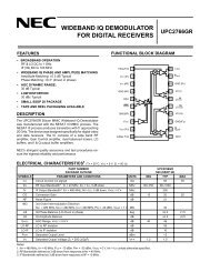
<strong>PS7341</strong>-1A,<strong>PS7341</strong>L-1A<br />
PACKAGE DIMENSIONS (in millimeters)<br />
<strong>PS7341</strong>-1A<br />
9.25±0.5<br />
6 5 4<br />
1 2 3<br />
TOP VIEW<br />
1. LED Anode<br />
2. LED Cathode<br />
3. NC<br />
4. MOS FET Drain<br />
5. MOS FET Source<br />
6. MOS FET Drain<br />
7.62<br />
6.5±0.5<br />
4.15±0.3<br />
3.5±0.3<br />
3.3±0.3<br />
0.5±0.1<br />
1.34±0.1<br />
0.25 M<br />
2.54<br />
0 to 15˚<br />
<strong>PS7341</strong>L-1A<br />
9.25±0.5<br />
6 5 4<br />
1 2 3<br />
TOP VIEW<br />
1. LED Anode<br />
2. LED Cathode<br />
3. NC<br />
4. MOS FET Drain<br />
5. MOS FET Source<br />
6. MOS FET Drain<br />
6.5±0.5<br />
3.5±0.3<br />
0.10 +0.10<br />
–0.05<br />
1.34±0.1<br />
0.25 M<br />
2.54<br />
0.9±0.25<br />
9.60±0.4<br />
2<br />
Data Sheet PN10306EJ02V0DS
<strong>PS7341</strong>-1A,<strong>PS7341</strong>L-1A<br />
<br />
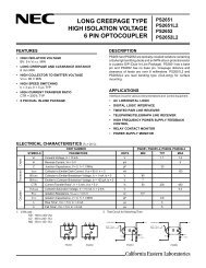
MARKING EXAMPLE<br />
No. 1 pin<br />
Mark<br />
<strong>PS7341</strong>-1A<br />
NL601<br />
Country Assembled<br />
Type Number<br />
Assembly Lot<br />
N L 6 01<br />
Week Assembled<br />
Year Assembled<br />
(Last 1 Digit)<br />
In-house Code<br />
(L: Pb-Free)<br />
Rank Code<br />
Data Sheet PN10306EJ02V0DS 3
<strong>PS7341</strong>-1A,<strong>PS7341</strong>L-1A<br />
<br />
ORDERING INFORMATION<br />
Part Number Order Number Solder Plating<br />
Specification<br />
Packing Style<br />
Safety Standard<br />
Approval<br />
Application Part<br />
Number *1<br />
<strong>PS7341</strong>-1A <strong>PS7341</strong>-1A-A Pb-Free Magazine case 50 pcs Standard products <strong>PS7341</strong>-1A<br />
<strong>PS7341</strong>L-1A <strong>PS7341</strong>L-1A-A (UL, BSI, CSA, SEMKO,<br />
<strong>PS7341</strong>L-1A-E3 <strong>PS7341</strong>L-1A-E3-A Embossed Tape 1 000 pcs/reel DEMKO, NEMKO,<br />
<strong>PS7341</strong>L-1A-E4 <strong>PS7341</strong>L-1A-E4-A FIMKO approved)<br />
*1 For the application of the Safety Standard, following part number should be used.<br />
4<br />
Data Sheet PN10306EJ02V0DS
<strong>PS7341</strong>-1A,<strong>PS7341</strong>L-1A<br />
ABSOLUTE MAXIMUM RATINGS (TA = 25°C, unless otherwise specified)<br />
Parameter Symbol Ratings Unit<br />
Diode Forward Current (DC) IF 50 mA<br />
Reverse Voltage VR 5.0 V<br />
Power Dissipation PD 50 mW<br />
Peak Forward Current *1 IFP 1 A<br />
MOS FET Break Down Voltage VL 400 V<br />
Continuous Connection A IL 150 mA<br />
Load Current *2 Connection B 200<br />
Connection C 300<br />
Pulse Load Current *3<br />
(AC/DC Connection)<br />
ILP 300 mA<br />
Power Dissipation PD 560 mW<br />
Isolation Voltage *4 BV 3 750 Vr.m.s.<br />
Total Power Dissipation PT 610 mW<br />
Operating Ambient Temperature TA −40 to +85 °C<br />
Storage Temperature Tstg −40 to +125 °C<br />
*1 PW = 100 µs, Duty Cycle = 1%<br />
*2 Conditions: IF ≥ 2 mA. The following types of load connections are available.<br />
Connection A<br />
Connection B<br />
Connection C<br />
6<br />
1<br />
2 5<br />
3<br />
4<br />
6<br />
1<br />
2<br />
5<br />
3 4<br />
1 6<br />
2<br />
5<br />
3<br />
4<br />
1<br />
2<br />
3<br />
6<br />
5<br />
4<br />
IL<br />
IL<br />
IL<br />
IL<br />
IL<br />
L<br />
L<br />
L<br />
L<br />
IL + IL<br />
+<br />
–<br />
–<br />
+<br />
+<br />
–<br />
VL (AC/DC)<br />
VL (DC)<br />
VL (DC)<br />
VL (DC)<br />
*3 PW = 100 ms, 1 shot<br />
*4 AC voltage for 1 minute at TA = 25°C, RH = 60% between input and output<br />
Pins 1-3 shorted together, 4-6 shorted together.<br />
Data Sheet PN10306EJ02V0DS 5
<strong>PS7341</strong>-1A,<strong>PS7341</strong>L-1A<br />
RECOMMENDED OPERATING CONDITIONS (TA = 25°C)<br />
Parameter Symbol MIN. TYP. MAX. Unit<br />
LED Operating Current IF 2 10 20 mA<br />
LED Off Voltage VF 0 0.5 V<br />
ELECTRICAL CHARACTERISTICS (TA = 25°C)<br />
Parameter Symbol Conditions MIN. TYP. MAX. Unit<br />
Diode Forward Voltage VF IF = 10 mA 1.2 1.4 V<br />
Reverse Current IR VR = 5 V 5.0 µA<br />
MOS FET Off-state Leakage Current ILoff VD = 400 V 0.03 1.0 µA<br />
Output Capacitance Cout VD = 0 V, f = 1 MHz 65 pF<br />
Coupled LED On-state Current IFon IL = 150 mA 2.0 mA<br />
On-state Resistance Ron1 IF = 10 mA, IL = 10 mA 20 30 Ω<br />
Ron2 IF = 10 mA, IL = 150 mA, t ≤ 10 ms 16 25<br />
Turn-on Time *1, 2 ton IF = 10 mA, VO = 5 V, RL = 2 kΩ, 0.35 1.0 ms<br />
Turn-off Time *1, 2 toff PW ≥ 10 ms 0.03 0.2<br />
Isolation Resistance RI-O VI-O = 1.0 kVDC 10 9 Ω<br />
Isolation Capacitance CI-O V = 0 V, f = 1 MHz 1.1 pF<br />
*1 Test Circuit for Switching Time<br />
Pulse Input<br />
IF<br />
VL<br />
Input<br />
50 %<br />
0<br />
Input monitor<br />
VO monitor<br />
VO = 5 V<br />
Output<br />
90 %<br />
Rin<br />
RL<br />
10 %<br />
ton<br />
toff<br />
<br />
*2 The turn-on time and turn-off time are specified as input-pulse width ≥ 10 ms.<br />
Be aware that when the device operates with an input-pulse width less than 10 ms, the turn-on time and turn-off<br />
time will increase.<br />
6<br />
Data Sheet PN10306EJ02V0DS
<strong>PS7341</strong>-1A,<strong>PS7341</strong>L-1A<br />
TYPICAL CHARACTERISTICS (TA = 25°C, unless otherwise specified)<br />
100<br />
MAXIMUM FORWARD CURRENT vs.<br />
AMBIENT TEMPERATURE<br />
300<br />
MAXIMUM LOAD CURRENT vs.<br />
AMBIENT TEMPERATURE<br />
Maximum Forward Current IF (mA)<br />
80<br />
60<br />
40<br />
20<br />
Maximum Load Current IL (mA)<br />
200<br />
100<br />
0<br />
–25<br />
0<br />
25<br />
50<br />
75<br />
85<br />
100<br />
0<br />
–25 0 25 50<br />
75<br />
85<br />
100<br />
Ambient Temperature TA (˚C)<br />
Ambient Temperature TA (˚C)<br />
Forward Voltage VF (V)<br />
1.8<br />
1.6<br />
1.4<br />
1.2<br />
1.0<br />
FORWARD VOLTAGE vs.<br />
AMBIENT TEMPERATURE<br />
IF = 50 mA<br />
30 mA<br />
20 mA<br />
10 mA<br />
5 mA<br />
1 mA<br />
Output Capacitance Cout (pF)<br />
200<br />
150<br />
100<br />
50<br />
OUTPUT CAPACITANCE vs.<br />
APPLIED VOLTAGE<br />
f = 1 MHz<br />
0.8<br />
–25 0 25 50 75<br />
100<br />
0<br />
20 40 60 80 100 120<br />
Ambient Temperature TA (˚C)<br />
Applied Voltage VD (V)<br />
Off-state Leakage Current ILoff (A)<br />
10 –5<br />
10 –6<br />
10 –7<br />
OFF-STATE LEAKAGE CURRENT vs.<br />
APPLIED VOLTAGE<br />
TA = 85 ˚C<br />
25 ˚C<br />
10 –8<br />
10<br />
0 100 200 300 400<br />
Applied Voltage VD (V)<br />
500<br />
Load Current IL (mA)<br />
LOAD CURRENT vs. LOAD VOLTAGE<br />
200<br />
100<br />
Load Voltage VL (V)<br />
IF = 10 mA<br />
–4.0 –2.0 0 2.0 4.0<br />
–100<br />
–200<br />
Remark The graphs indicate nominal characteristics.<br />
Data Sheet PN10306EJ02V0DS 7
<strong>PS7341</strong>-1A,<strong>PS7341</strong>L-1A<br />
Normalized On-state Resistance Ron<br />
NORMALIZED ON-STATE RESISTANCE vs.<br />
AMBIENT TEMPERATURE<br />
3.0<br />
2.5<br />
2.0<br />
1.5<br />
1.0<br />
0.5<br />
0.0<br />
–25 0<br />
25<br />
50<br />
Normalized to 1.0<br />
at TA = 25 ˚C,<br />
IF = 10 mA,<br />
IL = 10 mA<br />
75<br />
Ambient Temperature TA (˚C)<br />
100<br />
Number (pcs)<br />
ON-STATE RESISTANCE DISTRIBUTION<br />
30<br />
25<br />
20<br />
15<br />
10<br />
5<br />
0<br />
20 21<br />
On-state Resistance Ron (Ω)<br />
n = 50 pcs,<br />
IF = 10 mA,<br />
IL = 10 mA<br />
TURN-ON TIME vs. FORWARD CURRENT<br />
12<br />
VO = 5 V<br />
10<br />
TURN-OFF TIME vs. FORWARD CURRENT<br />
0.30<br />
VO = 5 V<br />
0.25<br />
Turn-on Time ton (ms)<br />
8<br />
6<br />
4<br />
Turn-off Time toff (ms)<br />
0.20<br />
0.15<br />
0.10<br />
2<br />
0.05<br />
0<br />
5<br />
10<br />
15<br />
20<br />
25<br />
30<br />
0<br />
5<br />
10<br />
15<br />
20<br />
25<br />
30<br />
Forward Current IF (mA)<br />
Forward Current IF (mA)<br />
30<br />
25<br />
TURN-ON TIME DISTRIBUTION<br />
n = 50 pcs,<br />
IF = 10 mA,<br />
VO = 5 V<br />
30<br />
25<br />
TURN-OFF TIME DISTRIBUTION<br />
n = 50 pcs,<br />
IF = 10 mA,<br />
VO = 5 V<br />
Number (pcs)<br />
20<br />
15<br />
10<br />
Number (pcs)<br />
20<br />
15<br />
10<br />
5<br />
5<br />
0<br />
0.3 0.4<br />
0<br />
0.03 0.05<br />
Turn-on Time ton (ms)<br />
Turn-off Time toff (ms)<br />
Remark The graphs indicate nominal characteristics.<br />
8<br />
Data Sheet PN10306EJ02V0DS
<strong>PS7341</strong>-1A,<strong>PS7341</strong>L-1A<br />
NORMALIZED TURN-ON TIME vs.<br />
AMBIENT TEMPERATURE<br />
NORMALIZED TURN-OFF TIME vs.<br />
AMBIENT TEMPERATURE<br />
Normalized Turn-on Time ton<br />
3.0<br />
2.5<br />
2.0<br />
1.5<br />
1.0<br />
0.5<br />
Normalized to 1.0<br />
at TA = 25 ˚C,<br />
IF = 10 mA,<br />
VO = 5 V<br />
Normalized Turn-off Time toff<br />
3.0<br />
2.5<br />
2.0<br />
1.5<br />
1.0<br />
0.5<br />
Normalized to 1.0<br />
at TA = 25 ˚C,<br />
IF = 10 mA,<br />
VO = 5 V<br />
0.0<br />
–25 0 25 50 75<br />
100<br />
0.0<br />
–25 0 25 50 75<br />
100<br />
Ambient Temperature TA (˚C)<br />
Ambient Temperature TA (˚C)<br />
Remark The graphs indicate nominal characteristics.<br />
Data Sheet PN10306EJ02V0DS 9
<strong>PS7341</strong>-1A,<strong>PS7341</strong>L-1A<br />
TAPING SPECIFICATIONS (in millimeters)<br />
Outline and Dimensions (Tape)<br />
2.0±0.1<br />
4.0±0.1<br />
1.5 +0.1<br />
–0<br />
1.75±0.1<br />
4.5 MAX.<br />
7.5±0.1<br />
16.0±0.3<br />
10.3±0.1<br />
1.55±0.1<br />
10.4±0.1<br />
4.0±0.1<br />
12.0±0.1<br />
0.3<br />
Tape Direction<br />
<strong>PS7341</strong>L-1A-E3<br />
<strong>PS7341</strong>L-1A-E4<br />
Outline and Dimensions (Reel)<br />
2.0±0.5<br />
2.0±0.5<br />
13.0±0.2<br />
R 1.0<br />
21.0±0.8<br />
330±2.0<br />
100±1.0<br />
17.5±1.0<br />
21.5±1.0<br />
Packing: 1 000 pcs/reel<br />
15.9 to 19.4<br />
Outer edge of<br />
flange<br />
10<br />
Data Sheet PN10306EJ02V0DS
<strong>PS7341</strong>-1A,<strong>PS7341</strong>L-1A<br />
RECOMMENDED SOLDERING CONDITIONS<br />
(1) Infrared reflow soldering<br />
• Peak reflow temperature<br />
• Time of peak reflow temperature<br />
• Time of temperature higher than 220°C<br />
• Time to preheat temperature from 120 to 180°C<br />
• Number of reflows<br />
• Flux<br />
260°C or below (package surface temperature)<br />
10 seconds or less<br />
60 seconds or less<br />
120±30 s<br />
Two<br />
Rosin flux containing small amount of chlorine (The flux with a<br />
maximum chlorine content of 0.2 Wt% is recommended.)<br />
Recommended Temperature Profile of Infrared Reflow<br />
Package Surface Temperature T (˚C)<br />
120˚C<br />
120±30 s<br />
(preheating)<br />
180˚C<br />
(heating)<br />
to 10 s<br />
to 60 s<br />
260˚C MAX.<br />
220˚C<br />
Time (s)<br />
(2) Wave soldering<br />
• Temperature<br />
• Time<br />
• Preheating conditions<br />
• Number of times<br />
• Flux<br />
260°C or below (molten solder temperature)<br />
10 seconds or less<br />
120°C or below (package surface temperature)<br />
One<br />
Rosin flux containing small amount of chlorine (The flux with a maximum chlorine<br />
content of 0.2 Wt% is recommended.)<br />
<br />
(3) Soldering by soldering iron<br />
• Peak temperature (lead part temperature)<br />
• Time (each pins)<br />
• Flux<br />
350°C or below<br />
3 seconds or less<br />
Rosin flux containing small amount of chlorine (The flux with a<br />
maximum chlorine content of 0.2 Wt% is recommended.)<br />
(a) Soldering of leads should be made at the point 1.5 to 2.0 mm from the root of the lead.<br />
(b) Please be sure that the temperature of the package would not be heated over 100°C.<br />
Data Sheet PN10306EJ02V0DS 11
<strong>PS7341</strong>-1A,<strong>PS7341</strong>L-1A<br />
<br />
(4) Cautions<br />
• To avoid quality degradation, assembling within 1 month after take this device out from covered pack is required.<br />
(Storage conditions 25°C, 65%RH MAX.)<br />
• Fluxes<br />
Avoid removing the residual flux with freon-based and chlorine-based cleaning solvent.<br />
<br />
USAGE CAUTIONS<br />
1. Protect against static electricity when handling.<br />
2. Avoid storage at a high temperature and high humidity.<br />
12<br />
Data Sheet PN10306EJ02V0DS
<strong>PS7341</strong>-1A,<strong>PS7341</strong>L-1A<br />
• The information in this document is current as of September, 2006. The information is subject to<br />
change without notice. For actual design-in, refer to the latest publications of NEC Electronics data<br />
sheets or data books, etc., for the most up-to-date specifications of NEC Electronics products. Not<br />
all products and/or types are available in every country. Please check with an NEC Electronics sales<br />
representative for availability and additional information.<br />
• No part of this document may be copied or reproduced in any form or by any means without the prior<br />
written consent of NEC Electronics. NEC Electronics assumes no responsibility for any errors that may<br />
appear in this document.<br />
• NEC Electronics does not assume any liability for infringement of patents, copyrights or other intellectual<br />
property rights of third parties by or arising from the use of NEC Electronics products listed in this document<br />
or any other liability arising from the use of such products. No license, express, implied or otherwise, is<br />
granted under any patents, copyrights or other intellectual property rights of NEC Electronics or others.<br />
• Descriptions of circuits, software and other related information in this document are provided for illustrative<br />
purposes in semiconductor product operation and application examples. The incorporation of these<br />
circuits, software and information in the design of a customer's equipment shall be done under the full<br />
responsibility of the customer. NEC Electronics assumes no responsibility for any losses incurred by<br />
customers or third parties arising from the use of these circuits, software and information.<br />
• While NEC Electronics endeavors to enhance the quality, reliability and safety of NEC Electronics products,<br />
customers agree and acknowledge that the possibility of defects thereof cannot be eliminated entirely. To<br />
minimize risks of damage to property or injury (including death) to persons arising from defects in NEC<br />
Electronics products, customers must incorporate sufficient safety measures in their design, such as<br />
redundancy, fire-containment and anti-failure features.<br />
• NEC Electronics products are classified into the following three quality grades: "Standard", "Special" and<br />
"Specific".<br />
The "Specific" quality grade applies only to NEC Electronics products developed based on a customerdesignated<br />
"quality assurance program" for a specific application. The recommended applications of an NEC<br />
Electronics product depend on its quality grade, as indicated below. Customers must check the quality grade of<br />
each NEC Electronics product before using it in a particular application.<br />
"Standard": Computers, office equipment, communications equipment, test and measurement equipment, audio<br />
and visual equipment, home electronic appliances, machine tools, personal electronic equipment<br />
and industrial robots.<br />
"Special": Transportation equipment (automobiles, trains, ships, etc.), traffic control systems, anti-disaster<br />
systems, anti-crime systems, safety equipment and medical equipment (not specifically designed<br />
for life support).<br />
"Specific": Aircraft, aerospace equipment, submersible repeaters, nuclear reactor control systems, life<br />
support systems and medical equipment for life support, etc.<br />
The quality grade of NEC Electronics products is "Standard" unless otherwise expressly specified in NEC<br />
Electronics data sheets or data books, etc. If customers wish to use NEC Electronics products in applications<br />
not intended by NEC Electronics, they must contact an NEC Electronics sales representative in advance to<br />
determine NEC Electronics' willingness to support a given application.<br />
(Note)<br />
(1) "NEC Electronics" as used in this statement means NEC Electronics Corporation and also includes its<br />
majority-owned subsidiaries.<br />
(2) "NEC Electronics products" means any product developed or manufactured by or for NEC Electronics (as<br />
defined above).<br />
M8E 02. 11-1<br />
Data Sheet PN10306EJ02V0DS 13
<strong>PS7341</strong>-1A,<strong>PS7341</strong>L-1A<br />
Caution<br />
GaAs Products<br />
This product uses gallium arsenide (GaAs).<br />
GaAs vapor and powder are hazardous to human health if inhaled or ingested, so please observe<br />
the following points.<br />
• Follow related laws and ordinances when disposing of the product. If there are no applicable laws<br />
and/or ordinances, dispose of the product as recommended below.<br />
1. Commission a disposal company able to (with a license to) collect, transport and dispose of<br />
materials that contain arsenic and other such industrial waste materials.<br />
2. Exclude the product from general industrial waste and household garbage, and ensure that the<br />
product is controlled (as industrial waste subject to special control) up until final disposal.<br />
• Do not burn, destroy, cut, crush, or chemically dissolve the product.<br />
• Do not lick the product or in any way allow it to enter the mouth.<br />
For further information, please contact<br />
NEC Compound Semiconductor Devices Hong Kong Limited<br />
E-mail: contact@ncsd-hk.necel.com<br />
Hong Kong Head Office TEL: +852-3107-7303 FAX: +852-3107-7309<br />
Taipei Branch Office TEL: +886-2-8712-0478 FAX: +886-2-2545-3859<br />
Korea Branch Office TEL: +82-2-558-2120 FAX: +82-2-558-5209<br />
NEC Electronics (Europe) GmbH http://www.eu.necel.com/<br />
TEL: +49-211-6503-0 FAX: +49-211-6503-1327<br />
<strong>California</strong> <strong>Eastern</strong> <strong>Laboratories</strong>, Inc. http://www.cel.com/<br />
TEL: +1-408-988-3500 FAX: +1-408-988-0279<br />
Compound Semiconductor Devices Division<br />
NEC Electronics Corporation<br />
URL: http://www.ncsd.necel.com/<br />
0604