A ZVC PWM half-bridge inverter with active clamping ... - IEEE Xplore
A ZVC PWM half-bridge inverter with active clamping ... - IEEE Xplore
A ZVC PWM half-bridge inverter with active clamping ... - IEEE Xplore

Create successful ePaper yourself
Turn your PDF publications into a flip-book with our unique Google optimized e-Paper software.
A ZVS <strong>PWM</strong> Half-Bridge Inverter <strong>with</strong> Active Clamping Technique Using the<br />
Reverse Recovery Energy of the Diodes<br />
Marcello Mezaroba", Denizar Cruz Martins** and Ivo Barbi**<br />
** UFSC - Federal University of Santa Catarina<br />
INEP - Power Electronics Institute<br />
P.O. Box 5119<br />
88040-970 Florianbpolis, SC, BRAZIL<br />
Phone: 55(48)331.9204 - Fax: 55(48)234.5422<br />
ivobarbi@inep.ufsc.br<br />
"SOCIESC - Educational Society of Santa<br />
Catarina<br />
IST - Superior Technology Institute<br />
P.O. Box 401<br />
89227-700 Joinville, SC, BRAZIL<br />
Phone: 55(47) 461-01 12 - Fax: 55447) 461-0134<br />
mezaroba@sociesc.com.br<br />
AB s T RA c T<br />
This paper presents a ZVS <strong>PWM</strong> Half-Bridge Inverter <strong>with</strong><br />
<strong>active</strong> voltage <strong>clamping</strong> technique using the reverse recovery<br />
energy of the diodes . The structure use only a single auxiliary<br />
switch and is particularly simple and robust. It is very attr<strong>active</strong><br />
for single-phase high power applications. Switching losses are<br />
reduced due to implementation of the simple <strong>active</strong> snubber<br />
circuit, that provides ZVS conditions for all switches, including<br />
the auxiliary one. Its main features are: Simple control strategy,<br />
robustness, lower weight and volume, lower harmonic distortion<br />
of the output current, and high efficiency. The principle of<br />
operation for steady-state conditions, mathematical analysis and<br />
experimental results from a laboratory prototype are presented.<br />
1. INTRODUCTION<br />
Whith athe appearance of the Bipolar Transistors in the 50s<br />
and posteriori the Mosfets in the SOS, <strong>PWM</strong> modulation<br />
techniques could be used together <strong>with</strong> the increase of the<br />
commutation frequency, <strong>with</strong> the aim to reduce the harmonic<br />
distortion in the output of the <strong>inverter</strong>s. These measures give<br />
some benefits like the reduction of the volume and weight of<br />
the filters and magnetic elements; nevertheless they cause<br />
some difficulties due to the high commutation losses in the<br />
switches, that reduce the efficiency of the converter, and the<br />
electromagnetic interference appearing. This events occur<br />
mainly in <strong>inverter</strong> topologies that use the <strong>bridge</strong><br />
configuration, where the main switch conduction provoke the<br />
reverse recovery phenomenon of the anti-parallel diode of the<br />
complementary switch.<br />
A great number of works have been developed by power<br />
electronics scientific community, <strong>with</strong> the aim to diminish<br />
these problems. They can be divided in two groups: passive<br />
techniques [6, 7, 8, 91 and <strong>active</strong> techniques [ 1, 2, ,3 IO].<br />
In the <strong>active</strong> techniques area, some researches were made<br />
recently using the reverse-recovery energy from the diodes to<br />
obtain soft commutation in the switches of the pre-regulated<br />
rectifiers <strong>with</strong> high power factor [4, 51.<br />
In this paper the analysis of a ZVS <strong>PWM</strong> <strong>half</strong>-<strong>bridge</strong><br />
<strong>inverter</strong> <strong>with</strong> <strong>active</strong> <strong>clamping</strong> technique using the reverse<br />
recovery energy of the diodes to improve the efficiency of the<br />
converter, is presented.<br />
This topology presents some advantages in comparison<br />
<strong>with</strong> the conventional soft commutation <strong>inverter</strong>s studied in<br />
the literature, which we can print out:<br />
Soft commutation in all load range;<br />
Simple topology <strong>with</strong> a low number of components;<br />
Use a classical <strong>PWM</strong> modulation;<br />
Auxiliary switch works <strong>with</strong> constant duty cycle in all<br />
operation stages;<br />
Use of slow and low cost rectifiers diodes;<br />
Low <strong>clamping</strong> voltage across the capacitor;<br />
Low current stress through the main switches;<br />
Simple design procedure <strong>with</strong> low restrictions;<br />
High efficiency.<br />
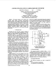
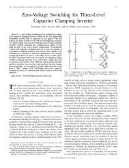
2. PROPOSED CIRCUIT<br />
The proposed circuit is shown in Fig. 1. It presents a <strong>half</strong><strong>bridge</strong><br />
<strong>inverter</strong> configuration, where Q1, 42 are the main<br />
switches, and Qa is the auxiliary switch. C1, C2 and Ca are<br />
the commutation capacitors.<br />
The snubber circuit is formed by one controlled switch,<br />
Qa, <strong>with</strong> antiparallel diode Da, one small inductor Ls and<br />
one <strong>clamping</strong> capacitor Cs. The capacitor Cs is responsible<br />
by the storage of the diode reverse recovery energy and by<br />
the <strong>clamping</strong> of switches voltage. The inductor Ls is<br />
responsible by the control of the dildt during the diode<br />
reverse recovery time. The auxiliary switch works <strong>with</strong><br />
constant duty cycle in all operation stage. One of the most<br />
advantage of this converter consists in the use of only one<br />
auxiliary switch, which provides the <strong>clamping</strong> of the voltage<br />
and the ZVS conditions for all switches, including the<br />
auxiliary switch in the snubber circuit.<br />
0-7803-7067-8/01/$10.00 02001 <strong>IEEE</strong> 1165
Fig: 1. Proposed Circuit.<br />
3. OPERATION STAGES (FOR THE FIRST HALF CYCLE)<br />
The principle operation of both semicycle of the <strong>inverter</strong><br />
load current is symmetrical. Thus, only for the first <strong>half</strong> cycle<br />
of the operation the circuit analysis will be made.<br />
To simplify the analysis, the following assumptions are<br />
made: the operation of the circuit is steady state; the<br />
components are considered ideal; excluding the reverse<br />
recovery of the diodes D1, D2. The voltage across the<br />
capacitor Cs, and the current in the output inductor Lc are<br />
considered constant during the switching period. The<br />
parameter E represents the total bus voltage (E=Vl+V2), and<br />
Vcs is the voltage across the <strong>clamping</strong> capacitor Cs.<br />
In the following paragraphs the operation stage of the first<br />
positive <strong>half</strong> cycle of the output current is described in detail.<br />
First stage (to-tl): During this interval the output current<br />
lout deliver energy to the source V2 via diode D2. At the<br />
same time, the additional current iLs flows around the mesh,<br />
formed by Ls, Qa, and Cs.<br />
Second stage (tl-t2): This stage starts when the auxiliary<br />
switch Qa is blocked. The current iLs begins the charge of<br />
the capacitor Ca from zero to E+Vcs (where E=Vl+V2), and<br />
discharges C1 from E+Vcs to zero.<br />
Third stage (t2-t3): At this stage the voltage across C1<br />
reaches zero, and it is <strong>clamping</strong> by the anti-parallel diode D1.<br />
So, the switch Q1 conducts <strong>with</strong> ZVS condition. At this<br />
moment, the voltage E = V1+V2 is applied across the<br />
inductor Ls and the currents iLs decrease linearly. The diode<br />
D1 conducts the current iLs, while D2 conducts the current<br />
iLs +lout.<br />
Fourth stage (t3-t4): It begins when the current iLs inverts<br />
its direction and flows through the switch Q1. The current iLs<br />
continues to decrease until inverting its direction of current of<br />
the diode D2, starting its reverse recovery phase. The<br />
inductor Ls limits the diLs/dt. In the end this stage the current<br />
in Ls is equal to Ir.<br />
Fifth stage (t4-t5): This stage starts when the diode D2<br />
finishes its reverse recovery phase. The current iLs begins the<br />
charge of the capacitor C2 from zero to E + Vcs and the<br />
discharge of Ca from E + Vcs to zero.<br />
Sixth stage (t5-t6): At this stage the voltage across the<br />
capacitor Ca reaches zero, and it is clamped by the diode Da.<br />
Thus, the auxiliary switch Qa conducts <strong>with</strong> zero-voltage<br />
switching. The current iLs increase, due the application of<br />
the voltage Vcs across the inductor Ls.This stage finishes<br />
when the current in Ls reaches zero.<br />
Seventh stage (t6-t7): This stage begins when the current iLs<br />
changes its direction and flows through the switch Qa. The<br />
current iLs continues to increase linearly.<br />
Eighth stage (t7-t8): At this stage the switch Q1 is blocked,<br />
and the current in Cs inverts its direction and flows through<br />
the diode Da. The capacitor C1 charges itself from zero to E<br />
+ Vcs and the capacitor C2 discharges itself from E + Vcs to<br />
zero.<br />
Ninth stage (&to): It begins when the voltage across the<br />
capacitor C2 reaches zero, and it is clamped by the diode D2.<br />
The current iLs continues increasing. This stage finishes<br />
when iLs is equal to lout, and flows through the auxiliary<br />
switch Qa, restarting the first operation stage.<br />
For the second <strong>half</strong> cycle the operation stage is analogous<br />
and can be described in an identical way.<br />
The main waveforms are shown in Fig. 2, and Fig.3. shows<br />
the main operation stages.<br />
1166
'<br />
1<br />
First stage (to-tl)<br />
Fourth stage (t3-t4)<br />
Second stage (tI-t2)<br />
-'r<br />
I<br />
L+<br />
Fifth stage (t4-tS)<br />
I<br />
Third stage (i2-t3)<br />
T "'<br />
I<br />
Fig. 3. Operationstage<br />
1<br />
s VI<br />
i I<br />
Ninth stage (t8-to)<br />
4. MATHEMATICAL ANALYSIS OF THE SOFT-SWITCHIh'G CIRCUIT<br />
To guarantee ZVS conditions, it is necessary, in the second<br />
stage, that the stored energy in the inductor Ls be sufficient to<br />
discharge the capacitor C1 and to charge Ca. Thus, by<br />
inspection of Fig. 3 (Interval t 1 -t2) the following condition<br />
can be formulated:<br />
Ls . If'<br />
2 (CU + CI)(E + Ifcs)'<br />
Where If is the maximum current in Cs, and Vcs is<br />
maintained constant during a switching period. Assuming<br />
Vcs
2Ls<br />
vcs = -[Ir + rout (I - D 11<br />
Ts<br />
The output current is given by:<br />
E.ma<br />
Iout = -.<br />
2 ’ Zout<br />
senw<br />
where Zout is the load impedance given by:<br />
Zout = JRoUt2 + (0. Lout)Z<br />
Rout - Load resistance<br />
Lc - Load inductance<br />
The duty cycle D can also be defined as:<br />
D = ma. sen@<br />
Where ma represent the modulation factor of amplitude.<br />
(7)<br />
(8)<br />
(9)<br />
(10)<br />
Combining Eqs. 7, 8 and 10 we obtain the expression of the<br />
Vcs voltage.<br />
senw . (1 - ma I sen,)] (1 1<br />
Where Ir is the peak reverse recovery current of the antiparallel<br />
diode, which can be given by:<br />
dl:<br />
E<br />
Ir= -.Qrr.-<br />
Ls<br />
Qrr - Reverse Recovery Charge<br />
From the analysis of the current behavior in the capacitor<br />
Cs , the expression of the current If can be obtained :<br />
If() = -.<br />
vcs<br />
Ls<br />
Ts - Iout - Ir<br />
Combining Eq. 11 <strong>with</strong> Eq. 13 and making some<br />
simplifications we obtain the expression that represents the<br />
evolution of the current If.<br />
Rc = 2,lSQ<br />
ma=0,9<br />
Load Resistance<br />
Modulation Factor<br />
B. CALCULATION OF THE AUXILIARY INDUCTORS.<br />
The auxiliary inductors are responsible for the dildt limit<br />
during the turn off of the main diodes. The dildt is directly<br />
related <strong>with</strong> the peak reverse recovery current lr of the<br />
antiparallel diodes. A “snappy” dildt produces a large<br />
amplitude voltage transient and contributes significantly to<br />
Electro-magnetic interference.<br />
In the design procedure it is chosen a dildt that is usually<br />
find in the diode data book. This is a simple way to obtain the<br />
diodes fundamental parameter for the design of the <strong>inverter</strong>.<br />
In such case the dildt chosen for this example was 4OAIus.<br />
Knowing that the current ramp rate is determined by the<br />
external circuit, thus:<br />
E 400V<br />
Ls = - =- = lopH<br />
di’ 40:;<br />
’ dr<br />
c. LOAD IMPEDANCE.<br />
The load impedance is obtained from Eq. 16<br />
(1 2) D. DIODE CHOOSE.<br />
For the performance of the <strong>inverter</strong> it is important to<br />
choose a slow diode. So, we opt to use the diode SEMIKRON<br />
SKKD 81/12, which has the following characteristics:<br />
(13) Vrrm = 1.2OOV Maximum Reverse Voltage<br />
Ifav = 80A<br />
Diode Average Current<br />
Qrr = 120yC Reverse Recovery Charge<br />
E. SWITCHING PERIOD<br />
E.ma E.ma2 ,<br />
If(t) = Ir+-----. senm---.sen-wt<br />
2 ’ Zout Zout<br />
1 1<br />
Ts=-=-- - 50p<br />
fs 20KHi<br />
To guarantee ZVS condition in all load range the minimum<br />
value of the current If obtained from Eq. 14 must be bigger<br />
F. REvERsERECovERycu~~T,<br />
than the value obtained from Eq. 2.<br />
The reverse recovery current is given by the Eq. 12.<br />
A. INPUTDATA<br />
E = 400V<br />
Vout = 127 V<br />
Pout = 73 KVA<br />
lout = 59A<br />
fs = 20KHz<br />
f = 60Hz<br />
Lc = 500 pH<br />
5. DESIGN EXAMPLE<br />
Bus Voltage<br />
RMS Output Voltage<br />
Output Power<br />
Output Current<br />
Switching Frequency<br />
Output Frequency<br />
Load Inductance<br />
G. CAPACITOR CLAMPING VOLTAGE BEHAVIOR<br />
Using a Eq. 1 I the curves described in Fig. 4 are obtained.<br />
For ma=0,9, the maximum <strong>clamping</strong> voltage is 42K<br />
We can observe that the voltage increment across the<br />
switches is smaller than conventional <strong>inverter</strong>.<br />
1168
vg<br />
40V<br />
36V<br />
32V<br />
I I I I I 1 1<br />
I<br />
28V<br />
I I I I 1<br />
0 n<br />
Fig 4. Capacitor Clamping Voltage Behavior<br />
H. CURRENT IF BEHA VIOR<br />
The current If behavior, obtained from Eq.12 and Eq.14,<br />
can be seen in Fig. 5.<br />
It is observed that the current If has a minimum point that<br />
is located in n/2, and the intensity of the current diminishes<br />
<strong>with</strong> the increase of the load. To guarantee <strong>ZVC</strong> condition in<br />
all range load, the minimum value of the current If, obtained<br />
from Eq. 14, must be bigger than the value of the traced<br />
straight line from Eq. 12.<br />
110A I I I ' I<br />
I<br />
I<br />
I<br />
Lout (500uH, Output Inductor)<br />
Rout (2.15 ; Output Resistor)<br />
B. EXPERIMENTAL WAVEFORMS<br />
In the figures presented below we can observe the<br />
experimental waveforms obtained from the laboratory<br />
prototype. Figs.6, 7 and 8 show the voltage and current in the<br />
switches.<br />
In Fig. 9 it can be observed the current in the commutation<br />
auxiliary inductor for a switching period.<br />
The voltage across the <strong>clamping</strong> capacitor Cs is shown in<br />
Fig.10. . We can note a very low voltage across Cs.<br />
The output voltage and current are presented in Fig. I 1.<br />
Fig. 12 show the efficiency as function of the load range.<br />
Tek Stop: 25.OMVS 148 A Y<br />
I<br />
Fig. 6. Voltage and current in Q 1, D 1 e C 1<br />
100V/div, SONdiv, 2us/div<br />
\ / I<br />
I qmrn ma=0.9 i<br />
I I , I I '<br />
n<br />
Fig. 5. Current If Behavior<br />
0'<br />
0<br />
6. EXPERIMENTAL RESULTS<br />
An <strong>inverter</strong> prototype rated 7.5kW operating <strong>with</strong> <strong>PWM</strong><br />
commutation was built to evaluate the proposed circuit. The<br />
main specifications and components are given below:<br />
A. PROTOTYPE SPECIFICATIONS<br />
Pout = 7500 W (Output Power)<br />
E = 400V (Input Voltage)<br />
Vout = 127V (Rms Output Voltage)<br />
f = 60Hz (Output Frequency)<br />
fs = 20 kHz (Switching Frequency)<br />
Ql,Q2, Qa (IGBT GA250TS60U)<br />
D1, D2, Da (SKKD81/12)<br />
C1, C2, Ca<br />
Ls<br />
cs<br />
(Intrinsic Capacitance =1.5nF)<br />
(IOuH each; Ferrite Core EE55/39; N=20<br />
turns, 87 wires #22AWG)<br />
(4 x 1000uF/350V; Electrolytic Capacitor)<br />
Fig. 7. Voltage and current in Q2, D2 eC2<br />
1 OOV/div, SONdiv, 2uddiv<br />
Tek stop: 10.OMsA<br />
455 Acp<br />
Fig. 8. Voltage and current in Qa, Da e Ca<br />
1 OOV/div, SONdiv, 1 Ous/div<br />
I<br />
1169
’<br />
Fig. 9. Current in Ls<br />
SONdiv. 1 Ouddiv<br />
7. CONCLUSIONS<br />
A ZVS <strong>PWM</strong> <strong>inverter</strong> <strong>with</strong> <strong>active</strong> voltage <strong>clamping</strong> using<br />
the reverse recovery energy of the diodes. The operation<br />
stages for steady-state condition, mathematical analysis, main<br />
waveforms and experimental results were presented. The<br />
experimental results show a low voltage in the <strong>clamping</strong><br />
capacitor. Switching losses are reduced due to the<br />
implementation of the simple <strong>active</strong> snubber circuit, that<br />
provides ZVS conditions for all the switches, including the<br />
auxiliary one. The reduced number of components and the<br />
simplicity of the structure increase its efficiency and<br />
reliability, and make it suitable for practical applications. The<br />
proposed circuit presents soft commutation for all load range,<br />
confirming the theoretical studies.<br />
. .. . ... .<br />
Fig. IO. Voltage in Cs<br />
1 OV/div, Sms/div<br />
Tel:nOp: lO.OM/S<br />
A<br />
100<br />
99<br />
98<br />
97<br />
96<br />
- 95<br />
$94<br />
2. 93<br />
.g 92<br />
91<br />
90<br />
89<br />
88<br />
87<br />
86<br />
8 5 1 I I I ~<br />
53 Acq5<br />
Ax2 1o.omv 5.<br />
Fig. 1 1. Output voltage and current<br />
SOV/div, SONdiv, Sms/div<br />
I<br />
iowi mw 3000 4000 soon 6ow 7uoo 8ow woo ium iiow<br />
Pout(W)<br />
Fig. 12. Efficiency over the output range.<br />
I<br />
8. REFERENCES<br />
BINGEN, G.; High Current and Voltage Transistor<br />
Utilization. Proceedings of First European Conference on<br />
Power Electronics and Applications, 1985 , pp. 1.15-<br />
1.20.<br />
McMURRAY, W. Resonant Snubbers <strong>with</strong> Auxiliary<br />
Switches. Conference Records of <strong>IEEE</strong> IAS Annual<br />
Meeting, 1990 pp.829-834.<br />
DE DONCKER, R. W.; LYONS, J. P. The Auxiliary<br />
Resonant Commuted Pole Converter. Conference<br />
Records of <strong>IEEE</strong> IAS Annual Meeting, 1990, pp. 1228-<br />
1235.<br />
BASSETT, John A.; New Zero Voltage Switching, High<br />
Frequency Boost Converter Topologv for Power Factor<br />
Correction. INTELELEC’95, pp 813-820.<br />
PIETKIEWICZ, A.; TOLLIK, D.; New High Power<br />
Single-phase Power Factor Corrector <strong>with</strong> So$-<br />
Switching. INTELEC’96, pp 114 - 119.<br />
[6] UNDERLAND, Tore Marvin ‘‘Switching Stress<br />
Reduction in Power Transistor Convertes”. <strong>IEEE</strong><br />
Industry Applications Society 1976, pp 383-391.<br />
[7] HOLTZ, J.; SALAMA, S. F.; WERNER, K.; “A<br />
Nondissipative Snubber Circuit for High-Power GTO-<br />
Inverters”. <strong>IEEE</strong> Industry Applications 1987, pp 613-<br />
618.<br />
[SI TARDIFF,D.; BARTON, T.H.; “A Summary of Resonant<br />
Snubbers Circuits for Transistors and GTOS“’ <strong>IEEE</strong><br />
1989, ~~1176-1180.<br />
[9] LANGER, H.G.; FREGIEN,G.; SKUDELNY, H.C. “A<br />
Low Loss Turn-on Turn-off Snubber for GTO-Inverters”.<br />
<strong>IEEE</strong> 1987, pp 607-612.<br />
[IO] CHERITI, A. “A Rugged So$ Commutated <strong>PWM</strong><br />
Znverterfor AC Drivers”. <strong>IEEE</strong> PESC 1990, pp 656-662.<br />
1170