
Create successful ePaper yourself
Turn your PDF publications into a flip-book with our unique Google optimized e-Paper software.
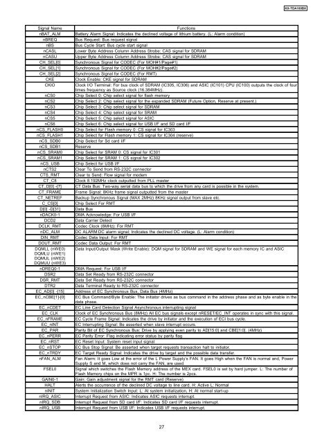
<strong>KX</strong>-<strong>TDA100BX</strong><br />
Signal Name<br />
nBAT_ALM<br />
nBREQ<br />
nBS<br />
nCASL<br />
nCASU<br />
CH_SEL[0]<br />
CH_SEL[1]<br />
CH_SEL[2]<br />
CKE<br />
CKIO<br />
nCS0<br />
nCS2<br />
nCS3<br />
nCS4<br />
nCS5<br />
nCS6<br />
nCS_FLASH0<br />
nCS_FLASH1<br />
nCS_SDB0<br />
nCS_SDB1<br />
nCS_SRAM0<br />
nCS_SRAM1<br />
nCS_USB<br />
nCTS2<br />
CTS_RMT<br />
CT_C8<br />
CT_D[0] -[7]<br />
CT_FRAME<br />
CT_NETREF<br />
C_CS[0]<br />
D[0] -D[31]<br />
nDACK0-1<br />
DCD2<br />
DCLK_RMT<br />
nDC_ALM<br />
DIN_RMT<br />
DOUT_RMT<br />
DQMLL (nWE0)<br />
DQMLU (nWE1)<br />
DQMUL (nWE2)<br />
DQMUU (nWE3)<br />
nDREQ0-1<br />
DSR2<br />
DSR_RMT<br />
DTR2<br />
EC_AD[0] -[15]<br />
EC_nCBE[1]-[0]<br />
EC_nCDET<br />
EC_CLK<br />
EC_nFRAME<br />
EC_nINT<br />
EC_PAR<br />
EC_nPERR<br />
EC_nRST<br />
EC_nSTOP<br />
EC_nTRDY<br />
nFAN_ALM<br />
FSEL0<br />
GAIN0-1<br />
HALT<br />
nINIT<br />
nIRQ_ASIC<br />
nIRQ_SDB<br />
nIRQ_USB<br />
Functions<br />
Battery Alarm Signal: Indicates the declined voltage of lithium battery. (L: Alarm condition)<br />
Bus Request: Bus request signal<br />
Bus Cycle Start: Bus cycle start signal<br />
Lower Byte Address Column Address Strobe: CAS signal for SDRAM<br />
Upper Byte Address Column Address Strobe: CAS signal for SDRAM<br />
Synchronous Signal for CODEC (For MOH#1/Page#1)<br />
Synchronous Signal for CODEC (For MOH#2/Page#2)<br />
Synchronous Signal for CODEC (For RMT)<br />
Clock Enable: CKE signal for SDRAM<br />
Clock I/O Terminal: For bus clock of SDRAM (IC305, IC306) and ASIC (IC101) CPU (IC100) outputs the clock of four<br />
times frequency as Source clock (16.384MHz).<br />
Chip Select 0: Chip select signal for flash memory<br />
Chip Select 2: Chip select signal for the expanded SDRAM (Future Option, Reserve at present.)<br />
Chip Select 3: Chip select signal for SDRAM<br />
Chip Select 4: Chip select signal for SRAM<br />
Chip Select 5: Chip select signal for ASIC<br />
Chip Select 6: Chip select signal for USB I/F and SD card I/F<br />
Chip Select for Flash memory 0: CS signal for IC303<br />
Chip Select for Flash memory 1: CS signal for IC304 (reserve)<br />
Chip Select for Sd card I/F<br />
Reserve<br />
Chip Select for SRAM 0: CS signal for IC301<br />
Chip Select for SRAM 1: CS signal for IC302<br />
Chip Select for USB I/F<br />
Clear To Send from RS-232C connector<br />
Clear to Send: Flow signal for modem<br />
Clock 8.192MHz clock outputted from PLL master<br />
CT Data Bus: Two-way serial data bus to which the drive from any card is possible in the system.<br />
Frame Signal: 8KHz frame signal outputted from the master<br />
Backup Synchronous Signal (MAX 2MHz) 8KHz signal output from slave etc.<br />
Chip Select For RMT<br />
Data Bus<br />
DMA Acknowledge: For USB I/F<br />
Data Carrier Detect<br />
Codec Clock (8MHz): For RMT<br />
DC ALARM:DC alarm signal; Indicates the declined DC voltage. (L: Alarm condition)<br />
Codec Data Input: For RMT<br />
Codec Data Output: For RMT<br />
Data Input/Output Mask (Write Enable): DQM signal for SDRAM and WE signal for each memory IC and ASIC<br />
DMA Request: For USB I/F<br />
Data Set Ready from RS-232C connector<br />
Data Set Ready from RS-232C connector<br />
Data Terminal Ready to RS-232C connector<br />
Address of EC Synchronous Bus, Data Bus (4MHz)<br />
EC Bus Command/Byte Enable: The initiator drives as bus command in the address phase and as byte enable in the<br />
data phase.<br />
EC Line Card Detection Signal Asynchronous interrupting signal<br />
Clock of EC Synchronous Bus (8MHz) All EC bus signals except nRESET/EC_INT operates in sync with this signal.<br />
EC Cycle Frame Signal: Indicates the drive by initiator and the execution of ECI bus cycle.<br />
EC Interrupting Signal: Be asserted when slave interrupt occurs.<br />
Parity Bit of EC Synchronous Bus: Drive by applying even parity to AD[15:0] and CBE[1:0]. (4MHz)<br />
EC Parity Error: Flag indicating error status by parity flag<br />
EC Reset Input: System reset input signal<br />
EC Bus Stop Signal: Be asserted when target requests transaction halt to initiator.<br />
EC Target Ready Signal: Indicates the drive by target and the possible data transfer.<br />
Fan Alarm: It goes Low at the error of the L Power Supply’s FAN. It goes High when the FAN is normal and, Power<br />
Supply S and M, which does not carry the FAN, are used.<br />
Signal which switches the Flash Memory address of the MEX card. FSEL0 is set by hard jumper. L: The number of<br />
Flash Memory chips on the MPR is 1pc. H: The number is 2pcs.<br />
Gain: Gain adjustment signal for the RMT card (Reserve)<br />
Alerts the occurrence of the declined DC voltage to line card. H: Active L: Normal<br />
System Initialization Switch Input: L: At system initialization, H: At normal start-up<br />
Interrupt Request from ASIC: Indicates ASIC requests interrupt.<br />
Interrupt Request from SD card I/F: Indicates SD card I/F requests interrupt.<br />
Interrupt Request from USB I/F: Indicates USB I/F requests interrupt.<br />
27