A Simple S-Parameter Test Set for the VNWA2 Vector ... - SDR-Kits
A Simple S-Parameter Test Set for the VNWA2 Vector ... - SDR-Kits
A Simple S-Parameter Test Set for the VNWA2 Vector ... - SDR-Kits

Create successful ePaper yourself
Turn your PDF publications into a flip-book with our unique Google optimized e-Paper software.
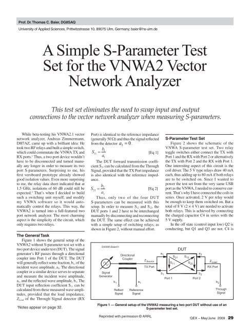
Prof. Dr. Thomas C. Baier, DG8SAQ<br />
University of Applied Sciences, Prittwitzstrasse 10, 89075 Ulm, Germany; baier@hs-ulm.de<br />
A <strong>Simple</strong> S-<strong>Parameter</strong> <strong>Test</strong><br />
<strong>Set</strong> <strong>for</strong> <strong>the</strong> <strong>VNWA2</strong> <strong>Vector</strong><br />
Network Analyzer<br />
This test set eliminates <strong>the</strong> need to swap input and output<br />
connections to <strong>the</strong> vector network analyzer when measuring S-parameters.<br />
While beta-testing his <strong>VNWA2</strong>.1 vector<br />
network analyzer, Andreas Zimmermann,<br />
DH7AZ, came up with a brilliant idea: He<br />
took two RF relays and built a simple switch,<br />
which could commutate <strong>the</strong> VNWA TX and<br />
RX ports. 1 Thus, a two port device wouldn’t<br />
have to be disconnected and turned manually<br />
any longer in order to measure its two<br />
port S-parameters. Surprising to me, his<br />
first veroboard prototype already showed<br />
good isolation values. Even more surprising<br />
to me, <strong>the</strong> relay data sheet indicated that at<br />
1.5 GHz, isolations of 60 dB could still be<br />
expected. 2 That’s when I decided to build<br />
such a switching unit myself, and modify<br />
my VNWA software so it would automatically<br />
control <strong>the</strong> relays. This way, <strong>the</strong><br />
<strong>VNWA2</strong> is turned into a full-featured two<br />
port network analyzer. The most charming<br />
aspect is <strong>the</strong> simplicity of <strong>the</strong> circuit, which<br />
only requires two relays.<br />
The General Task<br />
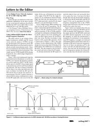
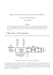
Figure 1 shows <strong>the</strong> general setup of <strong>the</strong><br />
<strong>VNWA2</strong> without S-parameter test set with a<br />
two port device under test (DUT). The signal<br />
generator’s RF passes through a directional<br />
coupler into Port 1 of <strong>the</strong> DUT. The DUT<br />
will generally reflect some fraction, b 1 , of <strong>the</strong><br />
incident wave amplitude, a 1 . The directional<br />
coupler or a similar device serves to separate<br />
and measure <strong>the</strong> incident wave amplitude,<br />
a 1 , and <strong>the</strong> reflected wave amplitude, b 1 . The<br />
DUT input reflection coefficient S 11 can be<br />
calculated from <strong>the</strong>se measured wave amplitudes,<br />
provided that <strong>the</strong> load impedance,<br />
Z Load of <strong>the</strong> Through Signal detector (RX<br />
1<br />
Notes appear on page 32.<br />
Port) is identical to <strong>the</strong> reference impedance<br />
(generally 50 Ω) and thus <strong>the</strong> signal reflected S-<strong>Parameter</strong> <strong>Test</strong> <strong>Set</strong><br />
from <strong>the</strong> detector a<br />
2<br />
= 0 .<br />
Figure 2 shows <strong>the</strong> schematic of <strong>the</strong><br />
b<br />
VNWA S-parameter test set. Two relay<br />
1<br />
S11<br />
= [Eq 1] toggle switches ei<strong>the</strong>r connect <strong>the</strong> TX with [Eq 1]<br />
b<br />
a1<br />
Port 1 and <strong>the</strong> RX with Port 2 or alternatively<br />
1<br />
S11<br />
The = DUT <strong>for</strong>ward transmission coefficient<br />
S 1 21 can be calculated from <strong>the</strong> Through One interesting aspect of this circuit is <strong>the</strong><br />
<strong>the</strong> TX with Port 2 and <strong>the</strong> RX with Port [Eq 1. 1]<br />
a<br />
Signal, provided that <strong>the</strong> TX Port impedance coil driver. The 5 V type relays draw 40 mA<br />
is also identical with <strong>the</strong> reference impedance.<br />
2<br />
each, thus adding up to 80 mA if both relays<br />
b<br />
S<br />
are to be switched on. Since I wanted to<br />
21<br />
= [Eq 2]<br />
b<br />
a<br />
power <strong>the</strong> test set from <strong>the</strong> very same USB<br />
1<br />
2<br />
S<br />
[Eq 2] port as <strong>the</strong> VNWA, I needed to conserve current.<br />
That’s why I have connected <strong>the</strong> coils in<br />
21<br />
= [Eq 2]<br />
a1<br />
Thus, only two of <strong>the</strong> four DUT series. Once activated, 2 V per relay would<br />
S-parameters can be measured with this be enough to keep <strong>the</strong>m switched on. But a<br />
setup. In order to measure S 12 and S 22 , <strong>the</strong> total of 8 V (2 × 4 V) are needed to activate<br />
DUT ports 1 and 2 have to be interchanged both relays. This is achieved by connecting<br />
manually by disconnecting and reconnecting <strong>the</strong> charged capacitor C4 in series with <strong>the</strong><br />
<strong>the</strong> DUT. The same effect can be achieved 5 V supply.<br />
with a simple setup of switching relays, as In <strong>the</strong> off state (control input low) Q2 is<br />
shown in Figure 2, without manual ef<strong>for</strong>t. conducting, but Q1 and Q3 are not. C4 is<br />
Figure 1 — General setup of <strong>the</strong> <strong>VNWA2</strong> measuring a two port DUT without use of an<br />
S-parameter test set.<br />
Reprinted with permission © ARRL<br />
QEX – May/June 2009 29
Figure 2 — Schematic of <strong>the</strong> VNWA S-<strong>Parameter</strong> <strong>Test</strong> <strong>Set</strong>.<br />
charged through D1 and Q2. When <strong>the</strong> control<br />
line goes high, Q1 and Q3 conduct, while<br />
Q2 goes into <strong>the</strong> off state. Q1 connects <strong>the</strong><br />
minus side of <strong>the</strong> now charged C4 to <strong>the</strong> supply<br />
voltage, which is thus added to <strong>the</strong> charge<br />
voltage of C4. The sum voltage is enough to<br />
activate both relays. After C4 is discharged<br />
through <strong>the</strong> relays, D1 takes over <strong>the</strong> reduced<br />
coil current. A current of 20 mA is enough<br />
to hold both relays in <strong>the</strong> on state. D2 is<br />
necessary to suppress high voltage induction<br />
voltage spikes, which could damage <strong>the</strong> driving<br />
transistors. I added R1 to fur<strong>the</strong>r reduce<br />
<strong>the</strong> holding current and as protection: For a<br />
very short moment during <strong>the</strong> activation, Q1<br />
and Q2 are conductive at <strong>the</strong> same time. R1<br />
serves to limit <strong>the</strong> current at this moment.<br />
Figure 3 shows <strong>the</strong> test set from <strong>the</strong> top.<br />
The two black relays can be seen with a<br />
shielding wall in between <strong>the</strong>m. The control<br />
signal and <strong>the</strong> power supply are provided<br />
through <strong>the</strong> 3.5 mm audio connector on <strong>the</strong><br />
left side. The whole circuit is built up on<br />
veroboard, which is covered with adhesive<br />
copper foil on <strong>the</strong> relay side.<br />
Figure 4 shows <strong>the</strong> test set from <strong>the</strong> bottom,<br />
hooked up to <strong>the</strong> <strong>VNWA2</strong>. The driver<br />
circuitry is assembled onto <strong>the</strong> veroboard<br />
from <strong>the</strong> bottom, in surface mount style. In<br />
order to achieve <strong>the</strong> highest possible isolation,<br />
<strong>the</strong> shielding wall protrudes through<br />
slots in <strong>the</strong> veroboard to <strong>the</strong> bottom, and RF<br />
wiring is done with semi rigid coax lines.<br />
Also, <strong>the</strong>re is a copper sheet shielding around<br />
<strong>the</strong> relay middle contact pins.<br />
Note, that I have tapped <strong>the</strong> power supply<br />
and <strong>the</strong> control line at <strong>the</strong> VNWA control<br />
connector, thus avoiding modifications<br />
of <strong>the</strong> VNWA itself. Also note <strong>the</strong> funny<br />
homebrewed biangular male-to-male SMA<br />
adapters, which allow to freely fit different<br />
connector spacings by changing <strong>the</strong> tilt<br />
angles.<br />
Figure 5 shows a wideband isolation<br />
measurement of <strong>the</strong> test set from TX to RX<br />
port with ports 1 and 2 disconnected. The<br />
isolation is only marginally worse than <strong>the</strong><br />
dynamic range of <strong>the</strong> <strong>VNWA2</strong> up into <strong>the</strong><br />
GHz range, and is thus sufficient <strong>for</strong> most<br />
two port measurements. Note that 60 dB of<br />
isolation is achieved at 1.2 GHz with a single<br />
switch, without shunt switches!<br />
Figure 6 shows a wideband transmission<br />
measurement of <strong>the</strong> test set from TX to RX<br />
port with ports 1 and 2 connected to each<br />
o<strong>the</strong>r. The
Figure 4 — The test set as seen from <strong>the</strong> bottom, hooked up to <strong>the</strong><br />
<strong>VNWA2</strong>. Note that <strong>the</strong> connection cable taps <strong>the</strong> 5 V dc power supply<br />
and <strong>the</strong> control line at <strong>the</strong> VNWA digital Sub D9 interface.<br />
Figure 3 — <strong>Test</strong> set as seen from top. The shielding wall between <strong>the</strong><br />
relays is most crucial <strong>for</strong> good isolation. The sheet metal box size is<br />
65 × 45 mm².<br />
Figure 5 — The isolation measurement of <strong>the</strong> test set from TX to RX<br />
port over 0 to 1.8 GHz with ports 1 and 2 isolated.<br />
Figure 6 — The transmission measurement of <strong>the</strong> test set from TX to<br />
RX port over 0 to 1.8 GHz with ports 1 and 2 connected to each o<strong>the</strong>r.<br />
Advantages of Using a <strong>Test</strong> <strong>Set</strong>,<br />
Error Correction<br />
The most obvious advantage of <strong>the</strong> test<br />
set is <strong>the</strong> fact that two port devices can be<br />
fully characterized without manually turning<br />
<strong>the</strong>m during <strong>the</strong> measurement. Thus, all four<br />
S-parameters (S 11 , S 21 , S 12 , S 22 ) can continuously<br />
be measured. This fact yields ano<strong>the</strong>r,<br />
less obvious, advantage: As discussed earlier<br />
in this article, S 11 and S 21 can be deduced<br />
from a <strong>for</strong>ward direction measurement only<br />
if <strong>the</strong> TX port impedance, Z Source , and <strong>the</strong><br />
RX port impedance Z Load , are both identical<br />
to <strong>the</strong> reference impedance (usually 50 Ω).<br />
If this is not <strong>the</strong> case, some of <strong>the</strong> transmitted<br />
signal, b 2 , is reflected at <strong>the</strong> RX port, is<br />
retransmitted through <strong>the</strong> DUT and adds to<br />
<strong>the</strong> reflected input signal, b 1 , which in turn<br />
gets reflected at <strong>the</strong> TX port again. Thus,<br />
in this case <strong>the</strong> results of <strong>the</strong> <strong>for</strong>ward measurement<br />
are influenced by all four DUT<br />
S-parameters as signals travel through <strong>the</strong><br />
DUT in both directions. The same holds true<br />
<strong>for</strong> <strong>the</strong> measurement in <strong>the</strong> reverse direction.<br />
If both directions are continuously measured,<br />
<strong>the</strong>n <strong>the</strong> effects of non ideal source and load<br />
impedances can be ma<strong>the</strong>matically corrected<br />
in an exact manner. This technique is known<br />
as 12-term error correction. 3<br />
Figure 7 shows <strong>the</strong> measured S 11 and<br />
S 22 of <strong>the</strong> through calibration standard. By<br />
definition, both reflection coefficients of <strong>the</strong><br />
through standard are zero. Traces S 11 and<br />
S 22 show simply corrected results, which are<br />
identical with <strong>the</strong> detector reflection coefficient<br />
caused by Z Load ≠ 50 Ω. Note that <strong>the</strong><br />
detector match is better than 25 dB over <strong>the</strong><br />
displayed span, which is quite good. Mem1<br />
and Mem2 show <strong>the</strong> same data 12-term corrected.<br />
The effect of imperfect load match<br />
has completely vanished and <strong>the</strong> measured<br />
data is dominated by noise. The rising noise<br />
Reprinted with permission © ARRL<br />
QEX – May/June 2009 31
Figure 7 — Impact of 12-term error correction on measured S 11 and<br />
S 22 of <strong>the</strong> through calibration standard. Traces S 11 and S 22 show<br />
simply corrected results, while Mem1 and Mem2 show <strong>the</strong> same data<br />
12-term corrected.<br />
Figure 8 — Transmission data of a monolithic crystal filter measured<br />
at a reference impedance of 50 Ω with various error correction<br />
schemes and <strong>the</strong>n recalculated to source and load impedances of<br />
3000 Ω.<br />
floor to <strong>the</strong> high frequency side reflects <strong>the</strong><br />
decreasing available signal strength of <strong>the</strong><br />
instrument.<br />
One should think that <strong>the</strong> effects of<br />
12-term correction are generally small,<br />
but <strong>the</strong>y can become large if <strong>the</strong> measured<br />
S-parameters are used in a system simulation.<br />
Figure 8 shows transmission data of a<br />
monolithic crystal filter measured with <strong>the</strong><br />
VNWA at a reference impedance of 50 Ω<br />
with various error correction schemes and<br />
<strong>the</strong>n recalculated to source and load impedances<br />
of 3000 Ω, which are <strong>the</strong> optimum filter<br />
matching conditions <strong>for</strong> a flat pass band.<br />
Note that <strong>the</strong> simple error correction<br />
scheme (trace S 21 ) shows distinct spikes in<br />
<strong>the</strong> filter pass band, while <strong>the</strong> 12-term corrected<br />
result (Mem4) is as smooth as can be.<br />
Also shown are two simple enhanced through<br />
correction schemes (Traces Mem1: ETC1;<br />
Mem2: ETC2), which only require measurements<br />
in one direction. They partly take into<br />
account non perfect matching conditions, but<br />
<strong>the</strong>y do neglect multiple reflections. ETC2<br />
can be obtained from <strong>the</strong> 12-term equations<br />
by setting S 22 = 0 <strong>for</strong> <strong>the</strong> <strong>for</strong>ward terms and<br />
S 11 = 0 <strong>for</strong> <strong>the</strong> backward terms. ETC1 is<br />
obtained from ETC2 by setting <strong>the</strong> detector<br />
impedance equal to <strong>the</strong> reference impedance<br />
(usually 50 Ω). The ETC corrections are better<br />
than <strong>the</strong> simple one, but worse than <strong>the</strong><br />
12-term correction.<br />
Summary and outlook<br />
I have described an easy to build automatic<br />
2 port S-parameter test <strong>for</strong> <strong>the</strong> <strong>VNWA2</strong>. In<br />
spite of its simplicity, it offers sufficiently<br />
high isolation and low insertion loss. The<br />
test set also allows application of <strong>the</strong> very<br />
accurate 12-term error correction scheme in<br />
a very simple manner. With a little imagination,<br />
<strong>the</strong> test set can easily be upgraded<br />
to include bias tee networks <strong>for</strong> measuring<br />
active components. The most recent VNWA<br />
software is capable of automatically controlling<br />
<strong>the</strong> test set. It can be found at my Web<br />
site. 4 The version of <strong>the</strong> VNWA software current<br />
as of <strong>the</strong> publication date of this article is<br />
also available <strong>for</strong> download from <strong>the</strong> ARRL<br />
QEX Web site. 5<br />
Thanks to Andreas Zimmermann,<br />
DH7AZ, <strong>for</strong> sharing his great test set idea<br />
and to Paul Kiciak <strong>for</strong> many fruitful discussions<br />
on error correction.<br />
Professor Dr. Thomas Baier MA teaches<br />
physics, ma<strong>the</strong>matics and electronics at<br />
<strong>the</strong> University of Applied Sciences in Ulm,<br />
Germany. Be<strong>for</strong>e his teaching assignment,<br />
he spent 10 years of work on research and<br />
development of surface acoustic wave filters<br />
<strong>for</strong> mobile communication with Siemens and<br />
EPCOS. He holds 10 patents.<br />
Tom, DG8SAQ, has been a licensed radio<br />
amateur since 1980. He prefers <strong>the</strong> soldering<br />
iron to <strong>the</strong> microphone, though. His interests<br />
span from microwave technology to microcontrollers.<br />
Lately, he has started Windows programming<br />
with Delphi. Tom spent one year in<br />
Oregon USA rock climbing and working on his<br />
master’s degree.<br />
Notes<br />
1<br />
Professor Dr. Thomas C. Baier, DG8SAQ,<br />
“A Small, <strong>Simple</strong>, USB-Powered <strong>Vector</strong><br />
Network Analyzer Covering 1 kHz to 1.3<br />
GHz,” QEX, Jan/Feb 2009, ARRL, pp 32 –<br />
36. See also www.arrl.org/qex/2009/01/<br />
Baier.pdf<br />
2<br />
Omron G6Y Relay, see www.omron.com/<br />
ecb/products/pdf/en-g6y.pdf<br />
3<br />
See, <strong>for</strong> example, Agilent AN 1287-3,<br />
“Applying Error Correction to Network<br />
Analyzer Measurements,” Application Note,<br />
http://cp.literature.agilent.com/litweb/<br />
pdf/5965-7709E.pdf<br />
4<br />
See www.mydarc.de/DG8SAQ/NWA.html<br />
5<br />
The VNWA software current as of <strong>the</strong> publication<br />
date of this article is available <strong>for</strong><br />
download from <strong>the</strong> ARRL QEX Web site. Go<br />
to www.arrl.org/qexfiles and look <strong>for</strong> <strong>the</strong><br />
file 5x09_Baier.zip.<br />
32 QEX – May/June 2009 Reprinted with permission © ARRL