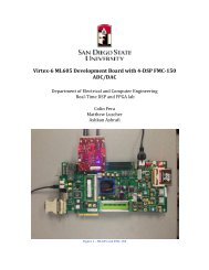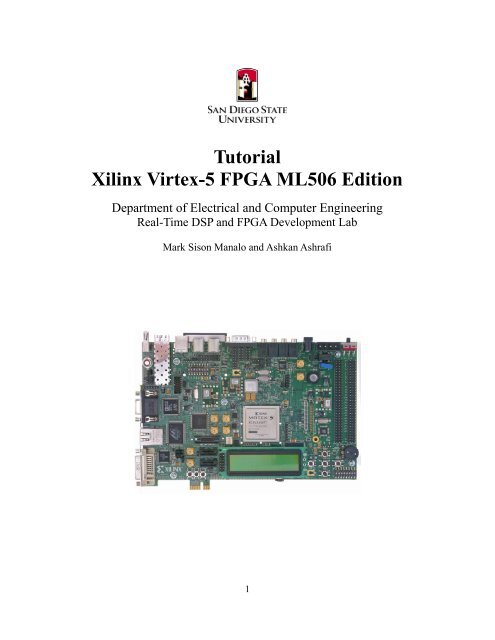
Tutorial Xilinx Virtex-5 FPGA ML506 Edition
Tutorial Xilinx Virtex-5 FPGA ML506 Edition
Tutorial Xilinx Virtex-5 FPGA ML506 Edition

Create successful ePaper yourself
Turn your PDF publications into a flip-book with our unique Google optimized e-Paper software.
<strong>Tutorial</strong><br />
<strong>Xilinx</strong> <strong>Virtex</strong>-5 <strong>FPGA</strong> <strong>ML506</strong> <strong>Edition</strong><br />
Department of Electrical and Computer Engineering<br />
Real-Time DSP and <strong>FPGA</strong> Development Lab<br />
Mark Sison Manalo and Ashkan Ashrafi<br />
1
Table of Contents<br />
Blank Page..................................................................................................................................................3<br />
Overview....................................................................................................................................................4<br />
About this tutorial.................................................................................................................................4<br />
Software needed ....................................................................................................................................4<br />
Hardware needed...................................................................................................................................4<br />
Setting up the <strong>ML506</strong> board.......................................................................................................................5<br />
The <strong>ML506</strong>............................................................................................................................................5<br />
Connecting the board.............................................................................................................................5<br />
Preparing the Compact Flash (Only when necessary).........................................................................10<br />
Running the <strong>Xilinx</strong> Demo.........................................................................................................................14<br />
Prerequisites.........................................................................................................................................14<br />
Programming the <strong>FPGA</strong> with a VHDL Design Using iMPACT – 2 bit greater than circuit....................16<br />
Summary..............................................................................................................................................16<br />
The VHDL Design...............................................................................................................................17<br />
Programming the <strong>FPGA</strong> using iMPACT.............................................................................................29<br />
Hardware Co-Sim with a System Generator created Design Using a Black Box – 2-bit greater-than from<br />
above.........................................................................................................................................................34<br />
Summary..............................................................................................................................................34<br />
Creating the Design..............................................................................................................................35<br />
Using <strong>Xilinx</strong> XPS and SDK to implement serial communication using the RS232 cable and a terminal<br />
program.....................................................................................................................................................56<br />
Summary..............................................................................................................................................56<br />
<strong>Xilinx</strong> XPS...........................................................................................................................................57<br />
<strong>Xilinx</strong> SDK..........................................................................................................................................70<br />
Play sound with a sine wave using the AC97 codec.................................................................................81<br />
Summary..............................................................................................................................................81<br />
<strong>Xilinx</strong> XPS...........................................................................................................................................81<br />
<strong>Xilinx</strong> SDK..........................................................................................................................................90<br />
Program the <strong>FPGA</strong>.............................................................................................................................104<br />
Programming your <strong>FPGA</strong> with the Compact Flash................................................................................106<br />
Summary............................................................................................................................................106<br />
Creating an .ace file...........................................................................................................................107<br />
Setting up the Compact Flash............................................................................................................112<br />
Conclusion..............................................................................................................................................114<br />
More Designs.....................................................................................................................................114<br />
2
Blank Page<br />
3
Overview<br />
About this tutorial<br />
This tutorial will help you familiarize yourself with <strong>Xilinx</strong>'s XtremeDSP Development<br />
Platform – <strong>Virtex</strong>-5 <strong>FPGA</strong> <strong>ML506</strong> <strong>Edition</strong>. Familiarity of C, VHDL and MATLAB/Simulink<br />
would help but it is not required. The ML505/506/507 are the same boards, only the <strong>FPGA</strong> is<br />
different so this tutorial will apply to all of them. Parts of this tutorial are taken from <strong>Xilinx</strong><br />
tutorials available here:<br />
http://www.xilinx.com/ml506<br />
http://www.xilinx.com/support/documentation/ml506.htm<br />
http://www.xilinx.com/products/boards/ml506/reference_designs.htm<br />
In addition to the <strong>Xilinx</strong> documents, the following websites and books were also referenced:<br />
http://www.fpgadeveloper.com/<br />
http://myfpgablog.blogspot.com/2009/12/sysgen-create-new-hwcosim-target-with.html<br />
http://academic.csuohio.edu/chu_p/rtl/fpga_vhdl.html<br />
Software needed<br />
• <strong>Xilinx</strong> ISE Design Suite (version 12.1 and 13.2 is used here)<br />
• <strong>Xilinx</strong> Platform Studio<br />
• <strong>Xilinx</strong> Software Development Kit<br />
• <strong>Xilinx</strong> System Generator<br />
• MATLAB/SIMULINK<br />
• Hyper Terminal / Tera Term / Putty or similar software (search it on Google and install)<br />
• msdosfs.exe with Windows XP (used for reformatting CF in case of file system<br />
corruption)<br />
Hardware needed<br />
• DVI cable or VGA cable with DVI adapter<br />
• RS232 cable for UART<br />
• <strong>Xilinx</strong> Platform USB cable<br />
• Speakers or headphones<br />
• Compact Flash reader (to load programs into the compact flash)<br />
4
Setting up the <strong>ML506</strong> board<br />
The <strong>ML506</strong><br />
Here is a picture of the <strong>ML506</strong> evaluation board with its components labeled.<br />
Connecting the board<br />
The board should already be connected in the <strong>FPGA</strong> lab. If not, please refer to the <strong>Xilinx</strong><br />
document titled: ml505_overview_setup.pdf<br />
For convenience, I will summarize it here.<br />
• Set the SW3 switches to 00010101 as shown in the picture:<br />
5
Bits 4-8 (10101) means that on power up, the <strong>ML506</strong> board will program the <strong>FPGA</strong> with<br />
the ACE file pointed to by bits 1-3 (in this case: 000). These ACE files are located on the<br />
compact flash. 000 means that the ACE file located in cfg0 of the compact flash will be<br />
programed into the <strong>FPGA</strong>. The factory compact flash files has the cfg0 folder containing a<br />
system_bootload .ace file. So if you want to load your own ACE file into folder cfg6<br />
(say). Then you would set SW3 to read 110 10101 if you want cfg7 then SW3 = 111<br />
10101 etc... (Search http://www.fpgadeveloper.com/ for a tutorial on creating your own<br />
ACE file). But for now lets stick the with factory default files.<br />
•<br />
6
• Set SW6 (on the back side of the board) to 11001010<br />
• Connect the <strong>Xilinx</strong> Platform Cable to PC4 JTAG<br />
• Connect the Serial cable (RS232) to the PC either directly or with a serial to USB adapter<br />
• Connect the Power cable to the board<br />
7
• Connect the DVI cable from the <strong>ML506</strong> to a monitor.<br />
• Insert the compact flash into the board.<br />
• Install a terminal program such as Tera Term Hyper Terminal or Putty and set it up with<br />
the following settings. (On my computer the Serial cable is connected to COM1, yours<br />
may differ)<br />
8
• Go to setup → serial port, and use these settings.<br />
9
Now your board should be ready to go. Don't forget to power it on when your ready.<br />
Preparing the Compact Flash (Only when necessary)<br />
The compact flash should already be formatted correctly as FAT12 or FAT16. After<br />
connecting the board insert the compact flash and power up the board. If the CF is not<br />
formatted correctly the LED labeled: SACE ERR would be a solid red color as shown in<br />
illustration 1.<br />
10
Illustration 1: SACE ERR, CF card is not being read correctly<br />
In this case, one would need to reformat the CF and place the factory default files back into it.<br />
<strong>Xilinx</strong> provides a tutorial on how to do this:<br />
http://www.xilinx.com/products/boards/ml506/ml506_12.1/images.htm<br />
However, my attempts at their tutorial using the dd tool did not work. You can try for yourself<br />
if you want. (For the records, I tried this using Windows 7 and I am getting either a nonexistent<br />
file error or a permissions error, even with administrative privileges)<br />
I managed to reformat the CF by another method, described below. (with the help of this:<br />
http://www.xilinx.com/support/answers/14456.htm)<br />
If you are going to reformat the CF, follow the directions carefully. Failure to do so might<br />
cause the primary hard drive to be erased .<br />
The following items are required:<br />
• Windows XP (I have not confirmed that it works with Windows 7, you can try though)<br />
• mkdosfs.exe (http://www.plunder.com/MKDOSFS-for-Windows-Format-drives-largerthan-32GB-as-FAT-or-FAT32-download-f738e8fe97.htm)<br />
• Compact flash reader (order at Newegg.com, or some other electronics store)<br />
• <strong>ML506</strong> factory CF files, go here:<br />
http://www.xilinx.com/products/boards/ml506/ml506_12.1/images.htm<br />
11
After inserting your CF card into your computer note its drive letter by clicking on Computer.<br />
In my case the drive letter is F: , note that the System ACE controller can only support up to<br />
2GB, the figure above is only for illustrative purposes. The 4GB CF that I have will not work.<br />
Add mkdosfs to your system path: Click start, right-click Computer → Properties →<br />
Advanced system settings → Environment Variables. Then edit the 'Path' variable to include<br />
the location of where you downloaded mkdosfs.exe. Google how to add to system path for<br />
more info.<br />
Then open up a command prompt in windows, preferably with administrative privileges (right<br />
click command prompt –> run as administrator).<br />
Type the following command:<br />
mkdosfs -v -F 16 F:<br />
Where 'F:' would be changed to your CF drive letter. Leave the first F as '-F'<br />
After this completes, copy and paste the CF factory files into the compact flash as shown:<br />
12
Once this is complete, right-click the compact flash and eject it.<br />
13
Insert the CF back into the <strong>ML506</strong> and turn on the power. Hopefully, you will have no red<br />
SACE ERR.<br />
No SACE ERR<br />
Running the <strong>Xilinx</strong> Demo<br />
Prerequisites<br />
• Make sure you have the board connected to the computer (see—connecting the board)<br />
• Insert the Compact Flash with the factory files loaded into it.<br />
• Connect some headphones or speakers to Line out.<br />
14
After connecting your board. Run Tera Term/HyperTerminal/Putty with the setting described in<br />
the section 'Connecting the Board '.<br />
15
Power up the board and it should start displaying text to the Tera Term window as shown<br />
below.<br />
You can run the demo programs by pressing a number on your PC keyboard that corresponds to<br />
your demo of choice.<br />
Also, this demo makes use of the monitor connected to your <strong>ML506</strong> via DVI or VGA adapter.<br />
Make sure you switch your screen input (press on the buttons in front of you monitor to access<br />
the menu) to the <strong>ML506</strong> so you can see the video output.<br />
Programming the <strong>FPGA</strong> with a VHDL Design Using iMPACT – 2<br />
bit greater than circuit<br />
Summary<br />
This tutorial will show you how to program the <strong>FPGA</strong> with a VHDL design created in ISE.<br />
Then we will use 4 switches and 1 led on the <strong>ML506</strong> board to simulate the design. We will<br />
not go over the VHDL code as it is beyond the scope of this tutorial. After finishing this<br />
tutorial, you should be able to program the <strong>FPGA</strong> with your own circuit design and connect it<br />
to some GPIO (general purpose input/output) pins.<br />
16
The VHDL Design<br />
Open up <strong>Xilinx</strong> ISE.<br />
17
Click File--> New Project.<br />
Set the location of your project file, to avoid any errors later on, make sure there are no spaces<br />
in the file path you choose.<br />
Then name your project something descriptive like : twobit_greaterthan.<br />
Make sure the top-level source is HDL.<br />
Click Next.<br />
18
Now setup the project settings for the <strong>ML506</strong> as shown below and click Next and Finish.<br />
A 2-bit greater-than circuit can be realized as a sum of products, namely,<br />
agreatb = a(1)b(1)' + a(0)b(1)'b(0)' + a(1)a(0)b(0)'<br />
where a and b are the 2-bit inputs and agreatb is the output.<br />
First we will write the VHDL file that implements the circuit, then we will connect inputs a<br />
and b to 4 switches and the output agreatb to an led using a universal constraints file.<br />
19
Highlight the xc5vsx50t in the Hierarchy window, then at the top menu click Project → New<br />
Source.<br />
20
Select VHDL module and name the file 'greater_2bit', click Next.<br />
21
In the define module screen change the architecture name to 'sop_arch' for sum-of-products<br />
architecture. We have two inputs, a and b, each two bits wide and one output 'agreatb'. Click<br />
Next and Finish.<br />
<strong>Xilinx</strong> should now have created a VHDL template for use to write our code in. If you don't<br />
see it double click on the file 'greater_2bit – sop_arch' in the hierarchy window.<br />
Change the architecture definition to this:<br />
architecture sop_arch of greater_2bit is<br />
begin<br />
signal p0, p1, p2 : std_logic;<br />
agreatb
p1
We are interested in these pin locations:<br />
24
At the top click on Project → New Source.<br />
Select Implementation Constraints File and name the file 'ml506_board'. Click Next and<br />
finish.<br />
25
Now you should see a blank file, if not, double-click on 'ml506_board.ucf' in the hierarchy<br />
window.<br />
Enter in the following code and save.<br />
26
Now that our code is finished we have to implement the design and generate the bitstream.<br />
Highlight 'greater_2bit -sop_arch' in the Hierarchy window, then in the processes window below it,<br />
double-click 'Implement Design' after it finishes double-click 'Generate Programming File' , this<br />
will generate the bistream needed to program the <strong>FPGA</strong>.<br />
27
After <strong>Xilinx</strong> finishes generating the programming file, you can find it inside your project<br />
directory.<br />
28
Programming the <strong>FPGA</strong> using iMPACT<br />
Now its time to program the <strong>FPGA</strong>. Close <strong>Xilinx</strong> ISE and open up iMPACT.<br />
29
Cancel all the initial prompts that come up.<br />
Turn on the <strong>ML506</strong>. If this is your first time turning it on, Windows might automatically<br />
install some drivers (allow it to, a restart maybe required).<br />
Double-click on 'Boundary Scan', then right-click on the empty plane and click 'Initialize<br />
Chain'. If you are getting errors about iMPACT unable to see your board, unplug the USB<br />
cable from your <strong>ML506</strong> and replug it to initiate some windows auto driver install.<br />
Cancel all the automatic prompts that come up.<br />
30
If all is well, you should see the JTAG chain with the <strong>Virtex</strong> 5 <strong>FPGA</strong> as well as some PROMs,<br />
ACE controller and CPLDs.<br />
Right-click on the <strong>FPGA</strong> (xc5vsx50t) and click 'Assign New Configuration File'<br />
then browse to your .bit file.<br />
31
It might prompt you to attach an SPI or BPI PROM, say no. Now right-click the <strong>FPGA</strong> and<br />
click 'Program'<br />
32
That's it! Your 2-bit greater-than circuit should now be operational. Input a is on switch 1 and<br />
2 of the GPIO DIP switch and input b is on switch 3 and 4. Toggle the switches (the tip of a<br />
mechanical pencil would help if the switches are too small for your fingers) and if a is greater<br />
than b (in binary) then the GPIO led0 will light up, else it will stay dark.<br />
33
Hardware Co-Sim with a System Generator created Design<br />
Using a Black Box – 2-bit greater-than from above<br />
Summary<br />
This builds off of a tutorial I found here:<br />
http://myfpgablog.blogspot.com/2009/12/sysgen-create-new-hwcosim-target-with.html<br />
We will use the 2-bit greater-than circuit that was designed in the previous topic 'Programming the<br />
<strong>FPGA</strong> using a VHDL design...' Also the <strong>Xilinx</strong> blockset in Simulink will be used to define our<br />
circuit inputs and outputs. The logic will be fulfilled by using the 'Black Box' block containing our<br />
greater-than VHDL code. The bitsream will be created with System Generator and the design will<br />
be simulated via hardware co-simulation.<br />
After finishing this tutorial you will be able to create a design using the <strong>Xilinx</strong> Blockset in<br />
Simulink and add a pre-made hdl design using a Black Box, then simulate the design on hardware<br />
within Simulink via hardware co-sim.<br />
34
Creating the Design<br />
First make sure that <strong>Xilinx</strong> System Generator is configured to use your version of MATLAB.<br />
Run the System Generator MATLAB configurator as administrator (right-click → run as<br />
administrator):<br />
35
Select the version of MATLAB you will be using and click ok:<br />
Now open up MATLAB and then Simulink.<br />
36
Once Simulink is open make a new model by clicking file → New → Model. Make a new folder<br />
on your local drive called 'GreaterThanCoSim' then save the model as 'greaterthan' into your newly<br />
created folder.<br />
38
In the Simulink Library Browser scroll down to <strong>Xilinx</strong> Blockset and double-click it, then double<br />
click on the Index tab. You should see all the available <strong>Xilinx</strong> blocks to create your design. Click<br />
and drag the block 'System Generator' into your model editor.<br />
39
Now we will create a new compilation target so we co-simulate with the <strong>ML506</strong>. In your model<br />
editor window, double-click on the 'System Generator' block. Under Compilation click Hardware<br />
Co-Simulation → New Compilation Target.<br />
40
Now the System Generator Board Description Builder should open up. Under Board Name type<br />
'<strong>ML506</strong>_twobitGreater'. Set the system clock Frequency to 100MHz and the pin location to AH15<br />
which is the USER_CLK pin.<br />
To find the Boundary Scan Position turn on your board and open up iMPACT (see previous tutorial)<br />
after initializing the JTAG chain you will see this:<br />
From here we see that the <strong>FPGA</strong> is in position 5 in the chain.<br />
41
Leave the board on and click 'Detect' to get the IR Lengths.<br />
On the Targetable Devices section, click Add → virtex5 → xc5vsx50t → -1 → ff1136<br />
It should now look similar to this:<br />
Now it is time to add our inputs and outputs. We will have two inputs each 2-bits wide and one<br />
output that is 1-bit wide.<br />
Under the 'Non-Memory-Mapped Ports' section click Add..<br />
Name the Port Name 'a' and select it as an input. Then for Pin LOC type: AG27 and click Add Pin.<br />
This will be the first bit of input a. Do the same for the second bit which is located on pin U25.<br />
After adding the second bit, click Save and Close.<br />
42
Now we do the same for input b.<br />
43
Click Save and Close, then click 'Add...' to add the output which will be sent to the GPIO led 0.<br />
Your screen should now look like this:<br />
44
Click Install to finish up the board description.<br />
45
Once the installation is complete, a new model editor will open up with this model (you can now<br />
close the 'System Generator Board Description Window'):<br />
In order to use this template we have to save it first. Click File → Save as and save it in the<br />
'GreaterThanCoSim' folder.<br />
Now highlight the template and drag it into your 'greaterthan' model.<br />
46
Next we will add the logic to our circuit model. You can do this using blocks by going to the<br />
'Simulink Library Browser' window and selecting the blocks you need. But since we already have<br />
our greater-than logic (in VHDL) we will use this to save some time.<br />
In order to use a VHDL design in Simulink, we need the 'Black Box' block located under <strong>Xilinx</strong><br />
Blockset → Index in the Simulink Library Broswer.<br />
So drag the Black Box into your model editor.<br />
48
After dragging in the box, a window will automatically appear requesting the entity description for<br />
the black box. Locate the VHDL file for the greater-than circuit and click open:<br />
49
Now your Black Box should have inputs and outputs as described by our VHDL file.<br />
Wire up your inputs and outputs to the Black Box by clicking and holding down the left mouse<br />
button.<br />
50
Double-click on the System Generator icon in your model editor and select the board description<br />
we just built under the Compilation tab.<br />
If you don't see it, close the System Generator window and save your model file. Then double-click<br />
on the Sytsem Generator icon again.<br />
51
After selecting '<strong>ML506</strong>_twobitGreater' click Generate. This may take a while (5-10 mins).<br />
Once completed, System Generator will show a Co-Sim block, drag this block into your model<br />
editor.<br />
We can now simulate our design. In your model editor, click Simulation → Configuration<br />
Parameters.<br />
Set the stop time to: inf<br />
Set Solver to : discrete<br />
52
Click ok.<br />
Make sure your board is on then in your model editor click the play button.<br />
54
Simulink will now program your <strong>FPGA</strong> (this may take a while). Wait until the model editor screen<br />
says running..<br />
55
Then you can toggle the GPIO switches to test the greater-than circuit, a picture is shown below:<br />
Illustration 2: a = '10' = 2 ; b = '01' = 1 ; thus a > b<br />
You can further customize this by adding more blocks to manipulate the signal. Here are some<br />
more complex design tutorials using a MAC FIR from <strong>Xilinx</strong>:<br />
http://www.xilinx.com/products/boards/ml506/ml506_12.1/dsp.htm<br />
<strong>Xilinx</strong> also provides a set of System Generator tutorials located in the installation directory. Mine is<br />
in<br />
C:\\<strong>Xilinx</strong>\12.1\ISE_DS\ISE\sysgen\examples<br />
Using <strong>Xilinx</strong> XPS and SDK to implement serial communication<br />
using the RS232 cable and a terminal program<br />
Summary<br />
This tutorial will show you how to use <strong>Xilinx</strong> XPS base system builder to create a base system<br />
package that connects the <strong>FPGA</strong> to its board peripherals such as the UART serial interface, GPIO<br />
LEDs, etc. After building the base system we will export it to <strong>Xilinx</strong> XPS where we can write the<br />
software to test the UART interface.<br />
Note: I have been experiencing some crashes with the <strong>Xilinx</strong> SDK version 12.1 in Windows 7.<br />
Version 13.1 and later is supposed to support Windows 7, so for this tutorial I will use <strong>Xilinx</strong> EDK<br />
version 13.2.<br />
56
<strong>Xilinx</strong> XPS<br />
First we will use XPS and the system builder wizard to add peripherals to our <strong>FPGA</strong>. This is done<br />
by creating a soft microprocessor to handle peripheral interfacing and communicate with the <strong>FPGA</strong>.<br />
First we will create a file system to organize our project files. Create a folder (I put mine in the<br />
local drive) and name it (make sure there are no spaces):<br />
ml506-edk-13-2<br />
57
Now within this folder make two empty folders name: edk, sdk<br />
We will store the board configuration files in the edk folder and the software files in the sdk folder.<br />
Open up <strong>Xilinx</strong> XPS (if you are using Windows 7, use Version 13.1 or later)<br />
58
Choose Base System Builder wizard:<br />
59
In the Project File section point it to the edk folder we created earlier and for the interconnect type<br />
choose PLB. For newer models of <strong>FPGA</strong> choose the AXI.<br />
Click OK.<br />
60
Choose new design and click Next.<br />
61
Choose the development board, in our case it is a <strong>Virtex</strong> 5 <strong>ML506</strong> Evaluation Platform and click<br />
next.<br />
62
The Base System Builder will create a soft processor for interfacing with the peripherals, choose<br />
Single-Processor System and click Next.<br />
63
Choose these default values for the processor specs and click Next.<br />
64
In the Peripheral window, leave it default. As you can see there are many peripherals connected to<br />
the MicroBlaze soft processor. We only need to create a base system once and we can reuse it for<br />
different projects so we might as well connect all the peripherals in case we need to use one for<br />
another project. Click Next.<br />
65
Click Next on the Cache window as we won't use any.<br />
66
The next page is the summary of our design, review it if you like and click Finish. (Make sure to<br />
check the Save Base System Builder Settings File box).<br />
67
The base system is now finished but before we can write some software for it we have to update<br />
the bitstream and export the board configurations to <strong>Xilinx</strong> SDK.<br />
Under Device Configuration click Update Bitstream, this process takes a long time (around half an<br />
hour).<br />
The console will say done when the bitstream update is complete:<br />
68
To export this project to the SDK, click Project → Export Hardware Design to SDK..<br />
Check the box to include the bitstream file we just generated and the BMM file. Then click Export<br />
Only: (This will created some files located in C:\ml506-edk-13-2\edk\SDK\SDK_Export\hw)<br />
This will enable the <strong>Xilinx</strong> SDK to use the hardware configuration we just described and create<br />
software to utilize them.<br />
69
<strong>Xilinx</strong> SDK<br />
Close <strong>Xilinx</strong> XPS and open <strong>Xilinx</strong> SDK:<br />
Point your workspace to the sdk folder we created at the beginning of this tutorial and click OK:<br />
70
Click File → New → <strong>Xilinx</strong> C Project:<br />
71
The <strong>Xilinx</strong> SDK will prompt you to specify a hardware platform. This is the file we exported in<br />
XPS and it contains all the hardware info of our board. Click Specify:<br />
72
Name the project UART_Test and point the hardware specification entry to the system.xml file<br />
that we exported. The bitstream and BMM entries should automatically fill after setting the<br />
system.xml entry: Click Finish<br />
73
In the next window, name the project hello_uart and select the Empty Application template, then<br />
click Next:<br />
74
Then name the board support package hello_uart_bsp and click Finish:<br />
<strong>Xilinx</strong> SDK will create a template for your new C project.<br />
75
Expand the 'src' folder under the 'hello_uart' project folder, then right-click on 'src' and click New<br />
→ Source File.<br />
Name the source file hello_uart.c and click Finish:<br />
A <strong>Xilinx</strong> text editor should come up (if it doesn't, double click hello_uart.c in the Project Explorer<br />
windows), delete all the auto generated comments and type in this code:<br />
#include <br />
int main()<br />
{<br />
xil_printf("Hello World");<br />
while(1) {<br />
}<br />
}<br />
return 0;<br />
Note: use xil_printf() when you can, printf () takes up too much memory space.<br />
76
Click save and <strong>Xilinx</strong> SDK should automatically build and compile your code and create a file<br />
called hello_uart.elf which you can use to program the <strong>FPGA</strong>.<br />
77
Now right-click on the hello_uart project and click Generate Linker Script<br />
78
Leave all the default settings and click Generate<br />
Note that if your .elf file is too big, you might have to increase the Heap and Stack size to<br />
accommodate your code:<br />
This .elf file, along with some system configuration bitstreams, is what you need to program the<br />
<strong>FPGA</strong> and run your software.<br />
79
Turn on the <strong>ML506</strong> and open up a serial terminal program such as HyperTerminal, TeraTerm,<br />
Putty etc.. Here I use TeraTerm, and set it up for serial communication on COM1 with 9600<br />
baude:<br />
Click on <strong>Xilinx</strong> Tools → Program <strong>FPGA</strong>:<br />
Point the Bitstream and BMM File entries to the files exported by Xilin XPS and under the<br />
microblaze_0 processor entry choose the hello_uart.elf file:<br />
Click Program and <strong>Xilinx</strong> SDK will combine the .bit, .bmm, .elf, files into a single bitstream<br />
called 'download.bit' located in C:\ml506-edk-13-2\sdk\UART_Test.<br />
80
I suggest you rename this file to something more meaningful like hellouart.bit.<br />
The <strong>FPGA</strong> is now programmed and you can see the results in the terminal window:<br />
Play sound with a sine wave using the AC97 codec<br />
Summary<br />
This tutorial makes use of the AC97 codec, LCD, UART (for text display) to play some sine waves<br />
through the line-in port of the AC97 interface. User instructions will be displayed to a COM serial<br />
window such as HyperTerminal or TeraTerm. Also some simple instruction will be displayed to the<br />
user via the on-board LCD screen.<br />
To avoid reinventing the wheel, we will use some <strong>Xilinx</strong> pre-made board configuration files and<br />
software.<br />
<strong>Xilinx</strong> XPS<br />
In order to use the on-board AC97 codec we would have to read the datasheet for the codec<br />
available here:<br />
http://www.xilinx.com/products/boards/ml505/datasheets/87560554AD1981B_c.pdf<br />
Then we would have to use our MicroBlaze softprocessor to setup AC97 according to its datasheet.<br />
But <strong>Xilinx</strong> has already done this for use so we can just use theirs and tailor it to our needs.<br />
First lets setup our file system to organize our project.<br />
81
Create a folder on the local drive called: AC97sine then within this folder create two more named<br />
sdk and xps.<br />
The <strong>Xilinx</strong> XPS files will be stored in the xps folder and the <strong>Xilinx</strong> SDK workspace will point to<br />
the sdk folder.<br />
First we need to download the pre-made <strong>Xilinx</strong> files.<br />
Get them here:<br />
http://www.xilinx.com/products/boards/ml506/ml506_12.1/bsb.htm<br />
Choose the <strong>ML506</strong> EDK Standard IP Design with Pcores Addition .zip file<br />
82
Extract the files somewhere like the desktop or a temp directory:<br />
83
Then copy these files and put them in your xps folder created earlier:<br />
84
Open up <strong>Xilinx</strong> XPS and cancel the first prompt:<br />
Click File → Open Project.. and browse to the ml506_bsb_system.xmp file in the xps folder and<br />
click Open:<br />
85
Since this <strong>Xilinx</strong> project was create with EDK version 12.1 and we are using version 13.2, <strong>Xilinx</strong><br />
will ask us to update the project. Click Yes:<br />
Click next on this first screen:<br />
86
Click Next on this window and the rest that follow:<br />
87
Finally, click Finish:<br />
88
After it finishes loading the files take a look at the peripherals. Notice that it has an ac97<br />
controller:<br />
Click on Device Configuration → Update Bitstream (this can take up to 30min):<br />
After this finishes click Project → Export Hardware Design to SDK and click Export Only:<br />
89
<strong>Xilinx</strong> SDK<br />
Close <strong>Xilinx</strong> XPS and open <strong>Xilinx</strong> SDK.<br />
Choose the workspace to be the sdk folder we created earlier and click OK<br />
Click File → New → <strong>Xilinx</strong> C Project.<br />
<strong>Xilinx</strong> will ask you to Specify a hardware platform, click Specify:<br />
90
Name the project ac97sine and browse to the exported files we created from <strong>Xilinx</strong> XPS and click<br />
Finish:<br />
91
Name the C project 'play_sine' and choose the Empty Application Template, then click Next:<br />
92
Name the board support package 'play_sine_bsp' and click Finish:<br />
93
The files I will be using can be found in:<br />
ml506_std_ip_pcores\sw\standalone<br />
Right-click the 'src' folder under the play_sine project and click New → Source File:<br />
94
Name the file 'play_sine.c' and click Finish:<br />
Delete all the auto-generated comments and put this in (copy and paste this code). The original<br />
version can be found in ml506_sdt_ip_pcores\sw\standalone\test_ac97. I cleaned it up and added<br />
the ability to choose different frequencies and use the LCD screen (its about 4 ½ pages long):<br />
#include <br />
#include <br />
#include "xio.h"<br />
#include "xuartns550_l.h"<br />
#include "sleep.h"<br />
#include "xparameters.h"<br />
#include "lcd.h"<br />
#include "memory_map.h"<br />
#define UART_CLOCK<br />
XPAR_XUARTNS550_CLOCK_HZ<br />
#if !SIM<br />
#define UART_BAUDRATE 9600 /* real hardware */<br />
#else<br />
#define UART_BAUDRATE (UART_CLOCK / 16 / 3) /* simulation */<br />
#endif<br />
95
* local prototypes */<br />
volatile int data_in_buf_len;<br />
int data_in_buf[19];<br />
volatile int dummy;<br />
volatile int cur_sound_len;<br />
volatile unsigned char *cur_sound_ptr;<br />
unsigned int sound_ptr;<br />
int c;<br />
int freq = 22;<br />
#define MY_AC97_BASEADDR<br />
XPAR_OPB_AC97_CONTROLLER_REF_0_BASEADDR<br />
#define AC97_InFIFO<br />
MY_AC97_BASEADDR<br />
#define AC97_OutFIFO<br />
MY_AC97_BASEADDR + 0x4<br />
#define AC97_FIFO_Status<br />
MY_AC97_BASEADDR + 0x8<br />
#define AC97_Control<br />
MY_AC97_BASEADDR + 0xC<br />
#define AC97_RegAddr<br />
MY_AC97_BASEADDR + 0x10<br />
#define AC97_RegRead<br />
MY_AC97_BASEADDR + 0x14<br />
#define AC97_RegWrite<br />
MY_AC97_BASEADDR + 0x18<br />
#define AC97_InFIFO_Full<br />
0x01<br />
#define AC97_InFIFO_Half_Full 0x02<br />
#define AC97_OutFIFO_Full 0x04<br />
#define AC97_OutFIFO_Empty 0x08<br />
#define AC97_Reg_Access_Finished 0x10<br />
#define AC97_CODEC_RDY<br />
0x20<br />
#define AC97_REG_ACCESS<br />
0x40<br />
#define AC97_Enable_In_Intr 0x01<br />
// AC97 CODEC Registers<br />
#define AC97_Reset<br />
0x00<br />
#define AC97_MasterVol<br />
0x02<br />
#define AC97_HeadphoneVol 0x04<br />
#define AC97_MasterVolMono 0x06<br />
#define AC97_Reserved0x08 0x08<br />
#define AC97_PCBeepVol<br />
0x0A<br />
#define AC97_PhoneInVol<br />
0x0C<br />
#define AC97_MicVol<br />
0x0E<br />
#define AC97_LineInVol<br />
0x10<br />
#define AC97_CDVol<br />
0x12<br />
#define AC97_VideoVol<br />
0x14<br />
#define AC97_AuxVol<br />
0x16<br />
#define AC97_PCMOutVol<br />
0x18<br />
#define AC97_RecordSelect 0x1A<br />
#define AC97_RecordGain<br />
0x1C<br />
#define AC97_Reserved0x1E 0x1E<br />
#define AC97_GeneralPurpose 0x20<br />
#define AC97_3DControl<br />
0x22<br />
#define AC97_PowerDown<br />
0x26<br />
#define AC97_ExtendedAudioID 0x28<br />
#define AC97_ExtendedAudioStat 0x2A<br />
#define AC97_PCM_DAC_Rate0 0x78<br />
#define AC97_PCM_DAC_Rate1 0x7A<br />
#define AC97_Reserved0x34 0x34<br />
#define AC97_JackSense<br />
0x72<br />
#define AC97_SerialConfig 0x74<br />
96
#define AC97_MiscControlBits<br />
#define AC97_VendorID1<br />
#define AC97_VendorID2<br />
0x76<br />
0x7C<br />
0x7E<br />
// Volume Constants<br />
#define AC97_VolMute 0x8000<br />
#define AC97_VolMax 0x0000<br />
#define AC97_VolMin 0x3F3F<br />
#define AC97_VolMid 0x1010<br />
void WriteAC97Reg( int reg_addr, int value) {<br />
XIo_Out32 (AC97_RegWrite, value);<br />
XIo_Out32 (AC97_RegAddr, reg_addr);<br />
usleep (10000);<br />
}<br />
int ReadAC97Reg( int reg_addr) {<br />
XIo_Out32 (AC97_RegAddr, reg_addr | 0x80);<br />
usleep (10000);<br />
return XIo_In32(AC97_RegRead);<br />
}<br />
void init_sound() {<br />
printf("Initializing AC97 CODEC...\r\n");<br />
// reset all reg's to known states (cause MUTE to all)<br />
WriteAC97Reg(AC97_Reset,0);<br />
usleep (1000);<br />
while (!(XIo_In32(AC97_FIFO_Status) & AC97_CODEC_RDY)) {};<br />
xil_printf ("PowerDown Reg State (Should be 0x000F) = %x \n\r", ReadAC97Reg<br />
(AC97_PowerDown));<br />
// turn on external amp<br />
xil_printf ("Turning on External Power Amp \n\r");<br />
WriteAC97Reg(AC97_JackSense,0x3F00); // set Jack Sense Pins<br />
// powerdown DAC and ADC temporarily<br />
WriteAC97Reg(AC97_PowerDown,0x0300);<br />
usleep (1000000);<br />
// initialize LCD and write to it<br />
LCDOn();<br />
LCDInit();<br />
LCDPrintString ("1. 400Hz 2. 1kHz", "3. 5kHz");<br />
xil_printf ("\n\r\n\rPick the frequency:\n\r");<br />
xil_printf ("1. 400Hz\n\r2. 1kHz\n\r3. 5kHz\n\r\n\r\n\r");<br />
while (!(XUartNs550_GetLineStatusReg(UART_BASEADDR) & 0x1));<br />
do {freq = XUartNs550_RecvByte(UART_BASEADDR); }<br />
// check for invalid choices<br />
while (((char) freq != '1') && ((char) freq != '2') && ((char) freq != '3'));<br />
if ((char) freq == '1') freq = 110;<br />
if ((char) freq == '2') freq = 44;<br />
if ((char) freq == '3') freq = 9;<br />
97
WriteAC97Reg(AC97_ExtendedAudioStat,1); // Enabling VRA mode<br />
WriteAC97Reg(AC97_PCM_DAC_Rate1, 48000); // sampling rate PLAY<br />
WriteAC97Reg(AC97_PCM_DAC_Rate0, 48000); // sampling rate rec<br />
xil_printf ("DAC sample rate= %d hz\n\r", ReadAC97Reg (AC97_PCM_DAC_Rate1));<br />
xil_printf ("ADC sample rate= %d hz\n\r", ReadAC97Reg (AC97_PCM_DAC_Rate0));<br />
xil_printf ("vendor id 1= %x\n\r", ReadAC97Reg (AC97_VendorID1));<br />
xil_printf ("vendor id 2= %x\n\r", ReadAC97Reg (AC97_VendorID2));<br />
// Turn back on power to ADC and DAC<br />
WriteAC97Reg(AC97_PowerDown,0x0000);<br />
usleep (100000);<br />
xil_printf ("PowerDown Reg State (Should be 0x000F) = %x \n\r", ReadAC97Reg<br />
(AC97_PowerDown));<br />
xil_printf ("Misc Control Bits = %x\n\r", ReadAC97Reg (AC97_MiscControlBits));<br />
XIo_Out32(AC97_Control, 0x00000003); // clear FIFOs<br />
XIo_Out32(AC97_InFIFO, 0);<br />
XIo_Out32(AC97_InFIFO, 0);<br />
XIo_Out32(AC97_InFIFO, 0);<br />
XIo_Out32(AC97_InFIFO, 0);<br />
XIo_Out32(AC97_InFIFO, 0);<br />
XIo_Out32(AC97_InFIFO, 0);<br />
XIo_Out32(AC97_InFIFO, 0);<br />
XIo_Out32(AC97_InFIFO, 0);<br />
XIo_Out32(AC97_InFIFO, 0);<br />
XIo_Out32(AC97_InFIFO, 0);<br />
XIo_Out32(AC97_InFIFO, 0);<br />
XIo_Out32(AC97_InFIFO, 0);<br />
XIo_Out32(AC97_InFIFO, 0);<br />
XIo_Out32(AC97_InFIFO, 0);<br />
XIo_Out32(AC97_InFIFO, 0);<br />
XIo_Out32(AC97_InFIFO, 0);<br />
// turn off digital loopback<br />
WriteAC97Reg(AC97_GeneralPurpose,0x0000);<br />
xil_printf ("General Purpose reg state = %x\n\r", ReadAC97Reg<br />
(AC97_GeneralPurpose));<br />
WriteAC97Reg(AC97_SerialConfig,0x7000);<br />
xil_printf ("config reg state = %x\n\r", ReadAC97Reg (AC97_SerialConfig));<br />
WriteAC97Reg(AC97_MasterVol, AC97_VolMid);<br />
WriteAC97Reg(AC97_HeadphoneVol, AC97_VolMid);<br />
WriteAC97Reg(AC97_MasterVolMono, AC97_VolMid);<br />
WriteAC97Reg(AC97_PCBeepVol, AC97_VolMute);<br />
WriteAC97Reg(AC97_PhoneInVol, AC97_VolMute);<br />
WriteAC97Reg(AC97_CDVol,<br />
AC97_VolMute);<br />
WriteAC97Reg(AC97_VideoVol, AC97_VolMute);<br />
WriteAC97Reg(AC97_AuxVol, AC97_VolMute);<br />
WriteAC97Reg(AC97_PCMOutVol, AC97_VolMid);<br />
WriteAC97Reg(AC97_RecordSelect, 0x0000);<br />
98
WriteAC97Reg(AC97_MicVol,<br />
WriteAC97Reg(AC97_LineInVol,<br />
}<br />
0x0040);<br />
AC97_VolMid);<br />
void play_sound(){<br />
int i;<br />
int j;<br />
xil_printf ("Play Start\n\r");<br />
sound_ptr = DDR_BASEADDR;<br />
WriteAC97Reg(AC97_RecordGain, AC97_VolMute);<br />
WriteAC97Reg(AC97_PowerDown, 0x0100);<br />
WriteAC97Reg(AC97_LineInVol, AC97_VolMute);<br />
i = 0;<br />
do {<br />
XIo_Out32(AC97_Control, 0x00000003); // clear FIFOs<br />
XIo_Out32(AC97_InFIFO, 0);<br />
XIo_Out32(AC97_InFIFO, 0);<br />
XIo_Out32(AC97_InFIFO, 0);<br />
XIo_Out32(AC97_InFIFO, 0);<br />
XIo_Out32(AC97_InFIFO, 0);<br />
XIo_Out32(AC97_InFIFO, 0);<br />
XIo_Out32(AC97_InFIFO, 0);<br />
XIo_Out32(AC97_InFIFO, 0);<br />
} while (XIo_In32(AC97_FIFO_Status) & 0x0040);<br />
while (1) {<br />
if (XIo_In32(AC97_FIFO_Status) & 0x0040) xil_printf ("play underrun\n\r");<br />
while (XIo_In32(AC97_FIFO_Status) & AC97_InFIFO_Half_Full) {};<br />
// The frequency is 44.1kHz so if we divide 44.1kHz by 22 we<br />
// get 2004.54 ~ 2kHz sine wave<br />
switch ((i) % freq) {<br />
case 0: j = 0 ; break;<br />
case 1: j = 9232; break;<br />
case 2: j = 17715; break;<br />
case 3: j = 24764; break;<br />
case 4: j = 29806; break;<br />
case 5: j = 32434; break;<br />
case 6: j = 32435; break;<br />
case 7: j = 29808; break;<br />
case 8: j = 24766; break;<br />
case 9: j = 17718; break;<br />
case 10: j = 9234; break;<br />
case 11: j = 3; break;<br />
case 12: j = -9229; break;<br />
case 13: j = -17713; break;<br />
case 14: j = -24762; break;<br />
case 15: j = -29805; break;<br />
case 16: j = -32434; break;<br />
case 17: j = -32435; break;<br />
case 18: j = -29809; break;<br />
case 19: j = -24768; break;<br />
case 20: j = -17720; break;<br />
case 21: j = -9237; break;<br />
}<br />
i = i+1;<br />
99
XIo_Out32(AC97_InFIFO, j);<br />
}<br />
}<br />
int main ()<br />
{<br />
XUartNs550_SetBaud(UART_BASEADDR, UART_CLOCK, UART_BAUDRATE);<br />
XUartNs550_SetLineControlReg(UART_BASEADDR, XUN_LCR_8_DATA_BITS);<br />
init_sound();<br />
while (1) {<br />
play_sound();<br />
}<br />
return 0;<br />
}<br />
100
After pasting in the above code, your window should look something like this:<br />
101
Next we need to add some header files.<br />
Go to the standalone folder:<br />
ml506_std_ip_pcores\sw\standalone<br />
and open the ml506_std_ip_pcores\sw\standalone\lib\src\sleep file.<br />
Highlight sleep.c and sleep.h and drag it into the src folder:<br />
Next, go to the ml506_std_ip_pcores\sw\standalone\include folder and drag the memory_map.h file<br />
into the src folder:<br />
Then, go to the ml506_std_ip_pcores\sw\standalone\lib\src\lcd_char folder and drage lcd.h and<br />
lcd.c into the src folder:<br />
102
Click Save and your project should start building and compiling.<br />
Right-click on the play_sine project and click Generate Linker Script, accept the default settings<br />
and click Generate overwriting existing files if asked:<br />
103
Program the <strong>FPGA</strong><br />
Turn on the <strong>ML506</strong> and open up a HyperTerminal or TeraTerm etc... I use putty here:<br />
Then in SDK click <strong>Xilinx</strong> Tools → Program <strong>FPGA</strong>.<br />
104
Make sure the bistream and BMM files point to the files you exported from XPS, then set your<br />
play_sine.elf file to be initialized onto the block RAM then click Program:<br />
The <strong>FPGA</strong> is now programmed. Look to the terminal window for the directions and choose your sine<br />
wave by typing on your PC keyboard:<br />
105
Some instructions are also displayed on the LCD:<br />
SDK will create a download.bit file located in : C:\AC97sine\sdk\ac97sine. I suggest you rename<br />
this to something like playsine.bit<br />
Programming your <strong>FPGA</strong> with the Compact Flash<br />
Summary<br />
You can save your programs on the compact flash so that when you turn on the <strong>ML506</strong> it will<br />
automatically run your program without having to open up iMPACT or <strong>Xilinx</strong> SDK to program it.<br />
To do this we need the bitstream for your project and then we convert it to a .ace file. Then we save<br />
this file into one of the configuration folders located in the file system of the compact flash. We<br />
then set the configuration mode on SW3 to correspond to the folder number we saved our .ace file<br />
into and turn on the board.<br />
We will use the bitsream created from the play sine wave tutorial. It is located in(on my computer):<br />
C:\AC97sine\sdk\ac97sine<br />
SDK names the file download.bit but I renamed it to playsine.bit<br />
106
Creating an .ace file<br />
This tutorial comes directly from this website:<br />
http://www.fpgadeveloper.com/2009/10/convert-bit-files-to-system-ace-files.html<br />
I will summarize it here for convenience:<br />
First add the <strong>Xilinx</strong> command: xmd<br />
to your system path (google 'how to add to path windows 7' if you don't know how):<br />
To get to this window right-click Computer, click Advanced system settings Environment<br />
Variables.., Edit the variable called 'Path' under System variables:<br />
107
Create a folder on your local drive called: SysACE<br />
Open up a text editor and copy and paste this code:<br />
@echo off<br />
if "%1" == "" goto error<br />
xmd -tcl ./genace.tcl -jprog -hw %1.bit -board ml505 -ace my_%1.ace<br />
goto end<br />
:error<br />
echo Makeace - by <strong>FPGA</strong> Developer http://www.fpgadeveloper.com<br />
echo.<br />
echo Usage: makeace bitfile (without .bit extension)<br />
echo Example: makeace project<br />
:end<br />
echo.<br />
108
Then save the file as makeace.bat into the SysACE folder:<br />
Now you should have this file in you SysACE folder:<br />
109
Now we need the bitstream of our project we want to convert to an ACE file. Lets use the<br />
playsine.bit from the previous tutorial (if you didn't rename it, it would be called download.bit).<br />
Copy and paste this file into the SysACE folder:<br />
Open up a windows command prompt:<br />
110
Type these commands to change directory to the SysACE folder:<br />
cd \SysACE<br />
Then to convert the file type:<br />
makeace playsine<br />
Once this finishes, several files will be created in the SysACE folder, we are interested in the<br />
my_playsine.ace file:<br />
111
Setting up the Compact Flash<br />
Make sure that your compact flash is properly formatted, see the beginning of this entire tutorial.<br />
Turn of the <strong>ML506</strong> and gently remove the compact flash. Insert the compact flash into your<br />
compact flash reader and open up the ML50X folder:<br />
112
Pick one of these folder (I chose cfg1) and open it:<br />
Inside you will notice some factory files, delete this file and replace it with the my_playsine.ace file<br />
we created (note: deleting this file will render the <strong>Xilinx</strong> Demo program inoperable):<br />
Safely eject, the compact flash:<br />
Then insert the compact flash back into the <strong>ML506</strong>.<br />
113
Since our file is in cfg1, we need to change the first three bits of SW3 to : 001 which is 1 in binary<br />
and leave the rest of the bits as: 10101.<br />
Here is a picture:<br />
Now turn on the board and your program should start automatically.<br />
You can put more designs into the other folders, just change the first three bits of SW3 to<br />
correspond to the folder number, then turn on the board.<br />
Conclusion<br />
More Designs<br />
By finishing this tutorial, you should be familiar with the many capabilities of the <strong>ML506</strong> and the<br />
various <strong>Xilinx</strong> softwares such as ISE and EDK. There are plenty of tutorials online and from<br />
<strong>Xilinx</strong>. Here are some links if you want to learn more:<br />
System Generator: http://www.xilinx.com/support/sw_manuals/sysgen_user.pdf<br />
<strong>Xilinx</strong> EDK: http://www.xilinx.com/support/documentation/sw_manuals/xilinx13_1/edk_ctt.pdf<br />
<strong>FPGA</strong> <strong>Tutorial</strong>s: http://www.fpgadeveloper.com/<br />
114