EE462L, Power Electronics, DC-DC Boost Converter Version ... - ECS
EE462L, Power Electronics, DC-DC Boost Converter Version ... - ECS
EE462L, Power Electronics, DC-DC Boost Converter Version ... - ECS

You also want an ePaper? Increase the reach of your titles
YUMPU automatically turns print PDFs into web optimized ePapers that Google loves.
<strong>EE462L</strong>, <strong>Power</strong> <strong>Electronics</strong>, <strong>DC</strong>-<strong>DC</strong> <strong>Boost</strong> <strong>Converter</strong><br />
<strong>Version</strong> Oct. 3, 2011<br />
Overview<br />
<strong>Boost</strong> converters make it possible to efficiently convert a <strong>DC</strong> voltage from a lower level to a<br />
higher level.<br />
Theory of Operation<br />
Relation Between V out and V in in Continuous Conduction<br />
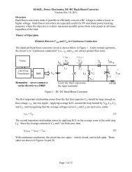
The idealized boost converter circuit is shown below in Figure 1. Under normal operation, the<br />
circuit is in “continuous conduction” (i.e., i L is never zero)<br />
i<br />
I L i d I out<br />
in<br />
Variac<br />
120/25Vac<br />
Transformer<br />
DBR<br />
Remember – never connect a variac directly<br />
toaDBR!<br />
V in<br />
Figure 1. <strong>DC</strong>-<strong>DC</strong> <strong>Boost</strong> <strong>Converter</strong><br />
L<br />
i C<br />
Leave the 10µF cap<br />
across the input terminals<br />
C<br />
0.01Ω<br />
+<br />
V out<br />
–<br />
The circuit is assumed to be lossless so that P in = P out , or<br />
V in • iLavg<br />
= Vout<br />
• Iout<br />
, where Lavg Iin<br />
i = . (1)<br />
Assuming continuous conduction, the circuit has two topologies – switch closed, and switch<br />
open. Both are shown in Figures 2a and 2b.<br />
+ v L<br />
−<br />
+ v L<br />
−<br />
i L<br />
I out<br />
i L<br />
I out<br />
V in<br />
L<br />
C<br />
i C<br />
+<br />
V out<br />
–<br />
V in<br />
L<br />
C<br />
i C<br />
+<br />
V out<br />
–<br />
Figure 2a. Switch Closed for DT<br />
Seconds<br />
Figure 2b. Switch Open for (1-D)T<br />
Seconds (Continuous Conduction)<br />
When the switch is closed, the diode is reverse biased and open, and i L increases at the rate of<br />
diL v V<br />
= L =<br />
in<br />
, 0 ≤ t ≤ DT , (2)<br />
dt L L<br />
and the inductor is “charging.” When the switch is open, the diode is forward biased, and i L<br />
decreases at the rate of<br />
Page 1 of 11
<strong>EE462L</strong>, <strong>Power</strong> <strong>Electronics</strong>, <strong>DC</strong>-<strong>DC</strong> <strong>Boost</strong> <strong>Converter</strong><br />
<strong>Version</strong> Oct. 3, 2011<br />
diL<br />
dt<br />
vL<br />
Vin<br />
−Vout<br />
= = , DT < t < T , (3)<br />
L L<br />
and the inductor is “discharging.” The inductor voltage is shown in Figure 3.<br />
V in<br />
0<br />
Vin − V out<br />
Figure 3. Inductor Voltage in Continuous Conduction<br />
Because of the steady-state inductor principle, the average voltage v L across L is zero. Since v L<br />
has two states, both having constant voltage, the average value is<br />
( V )<br />
in DT + ( Vin<br />
−Vout<br />
T<br />
)(1 − D)<br />
T<br />
= 0 ,<br />
so that<br />
Vin D + Vin<br />
−Vout<br />
−VinD<br />
+ Vout<br />
D = 0 .<br />
Simplifying the above yields the final input-output voltage expression<br />
Vout<br />
Vin<br />
= . (4)<br />
1 − D<br />
The graph of i L is shown in Figure 4.<br />
Inductor Current in Continuous Conduction<br />
Δ I<br />
T<br />
i<br />
L max<br />
i Lavg<br />
i<br />
L min<br />
= i<br />
= i<br />
Lavg<br />
Lavg<br />
ΔI<br />
+<br />
2<br />
ΔI<br />
−<br />
2<br />
DT<br />
(1–D)T<br />
Figure 4. Inductor Current Waveform for Continuous Conduction<br />
Page 2 of 11
<strong>EE462L</strong>, <strong>Power</strong> <strong>Electronics</strong>, <strong>DC</strong>-<strong>DC</strong> <strong>Boost</strong> <strong>Converter</strong><br />
<strong>Version</strong> Oct. 3, 2011<br />
From (2),<br />
diL<br />
dt<br />
Vin<br />
ΔI<br />
= = ,<br />
L DT<br />
so that<br />
Vin<br />
VinD<br />
Δ I = • DT = , (5)<br />
L Lf<br />
where f is the switching frequency.<br />
The boundary of continuous conduction is when<br />
T<br />
i L min = 0, as shown in Figure 5.<br />
Δ I<br />
iL max = 2I Lavg<br />
i Lavg<br />
i<br />
L min = 0<br />
DT<br />
(1–D)T<br />
Figure 5. Inductor Current at the Boundary of Continuous Conduction<br />
Using Figure 5 and the “inductor discharging” slope from (3),<br />
so that<br />
( V −V<br />
)( 1−<br />
D) V −V<br />
( 1−<br />
D)<br />
out in<br />
in in<br />
VinD<br />
Δ I =<br />
=<br />
=<br />
= 2I<br />
Lavg , (6)<br />
L f L f L f<br />
boundary<br />
boundary<br />
boundary<br />
L<br />
boundary<br />
VinD<br />
= . (7)<br />
2I<br />
f<br />
Lavg<br />
From (1),<br />
I Lavg = I in . (8)<br />
Substituting into (8) into (7) yields<br />
Page 3 of 11
<strong>EE462L</strong>, <strong>Power</strong> <strong>Electronics</strong>, <strong>DC</strong>-<strong>DC</strong> <strong>Boost</strong> <strong>Converter</strong><br />
<strong>Version</strong> Oct. 3, 2011<br />
Lboundary<br />
VinD<br />
= . (9)<br />
2Iin<br />
f<br />
Because the maximum value of D is 1, then<br />
Vin<br />
L > . (10)<br />
2Iin<br />
f<br />
will guarantee continuous conduction for all D. Note in (9) and (10) that continuous conduction<br />
can be achieved more easily when I out and f are large.<br />
Discontinuous Conduction<br />
At low load, the converter may slip into the discontinuous conduction mode. Referring back to<br />
Figure 2b, this occurs when the inductor current coasts to zero. At that moment, the capacitor<br />
attempts to reverse i L and “backfeed” the inductor, but the diode prevents current reversal. Thus,<br />
the diode opens, and the circuit assumes the topology shown in Figure 6 until the switch closes<br />
again. During this third state, all load power is provided by the capacitor.<br />
+ 0 –<br />
0<br />
I out<br />
V in<br />
L<br />
C<br />
+<br />
V out<br />
–<br />
Figure 6. Third State for Discontinuous Conduction<br />
Once discontinuous, the voltage across the inductor is zero. The corresponding voltage<br />
waveform is shown in Figure 7.<br />
V in<br />
Discontinuous<br />
Vin − V out<br />
0<br />
Figure 7. Inductor Voltage in Discontinuous Conduction<br />
Page 4 of 11
<strong>EE462L</strong>, <strong>Power</strong> <strong>Electronics</strong>, <strong>DC</strong>-<strong>DC</strong> <strong>Boost</strong> <strong>Converter</strong><br />
<strong>Version</strong> Oct. 3, 2011<br />
Current Waveforms in Continuous Conduction<br />
Continuous current waveforms are shown below.<br />
Δ I<br />
T<br />
Inductor<br />
i<br />
= i<br />
L max Lavg<br />
i Lavg = I in<br />
i<br />
L min<br />
= i<br />
Lavg<br />
ΔI<br />
+<br />
2<br />
ΔI<br />
−<br />
2<br />
DT<br />
(1–D)T<br />
Δ I<br />
ΔI<br />
MOSFET<br />
iL<br />
max = iLavg<br />
+<br />
2<br />
i Lavg = I in<br />
ΔI<br />
iL<br />
min = iLavg<br />
−<br />
2<br />
Δ I<br />
0<br />
ΔI<br />
i<br />
Diode<br />
L max = iLavg<br />
+<br />
2<br />
i Lavg = I in<br />
ΔI<br />
iL<br />
min = iLavg<br />
−<br />
2<br />
0<br />
Capacitor ( i<br />
C<br />
= i − I )<br />
L<br />
out<br />
ΔI<br />
iLavg − I out<br />
+ 2<br />
out<br />
Δ I<br />
0<br />
iLavg<br />
− Iout<br />
= Iin<br />
− I<br />
ΔI<br />
iLavg − − I out 2<br />
− I out<br />
(Note – compared to the other waveforms shown above, Δ I is exaggerated in the figure to<br />
illustrate how the capacitor current can be negative in both DT and (1–D)T regions)<br />
Figure 8. Current Waveforms for Continuous Conduction<br />
Page 5 of 11
<strong>EE462L</strong>, <strong>Power</strong> <strong>Electronics</strong>, <strong>DC</strong>-<strong>DC</strong> <strong>Boost</strong> <strong>Converter</strong><br />
<strong>Version</strong> Oct. 3, 2011<br />
Current Ratings in Continuous Conduction<br />
Conservative current ratings for the inductor in continuous conduction correspond to the<br />
situation where<br />
Δ Imax = 2I in , (11)<br />
which, as explained in the Buck <strong>Converter</strong> experiment, yields<br />
1 2<br />
2<br />
⎛ ⎞<br />
=<br />
2 +<br />
2 1<br />
I Lrms, max Iin<br />
( 2Iin<br />
) = Iin<br />
⎜1<br />
+ ⎟ , (12)<br />
12<br />
⎝ 3 ⎠<br />
so that<br />
2<br />
I Lrms , max = I in . (13)<br />
3<br />
Conservative current ratings for the MOSFET and diode are when D is large, so that (13) applies<br />
for them also.<br />
To determine the rms current through C, consider the capacitor current in Figure 8, and the<br />
worst-case scenario in Figure 9.<br />
2 I<br />
−<br />
in I out<br />
0<br />
Iin − I out<br />
DT<br />
(1–D)T<br />
Figure 9. Maximum Ripple Current Case for Capacitor Current<br />
When the switch is closed, the capacitor current is − Iout<br />
. When the switch is open, the<br />
capacitor current is iL<br />
− Iout<br />
. If the “switch closed” interval lasted for the entire T, the squared<br />
2<br />
rms value would be I out . If the “switch open” interval lasted for the entire T, the rms value<br />
would be, for the maximum ripple case, 2 1<br />
( I in − Iout<br />
) + ( 2Iin<br />
) 2 . The time-weighted average<br />
12<br />
of the two gives the squared rms current<br />
−<br />
I out<br />
Page 6 of 11
<strong>EE462L</strong>, <strong>Power</strong> <strong>Electronics</strong>, <strong>DC</strong>-<strong>DC</strong> <strong>Boost</strong> <strong>Converter</strong><br />
<strong>Version</strong> Oct. 3, 2011<br />
2 2<br />
⎛<br />
2 1 2 ⎞<br />
I Crms = DIout<br />
+ ( 1−<br />
D)<br />
• ⎜(<br />
Iin<br />
− Iout<br />
) + ( 2Iin<br />
) ⎟ . (14)<br />
⎝<br />
12 ⎠<br />
Now, substituting in I = I ( 1−<br />
D)<br />
yields<br />
out<br />
in<br />
2 2 2 ⎛<br />
2 1 2 ⎞<br />
I Crms = DIin<br />
( 1−<br />
D)<br />
+ (1 − D)<br />
• ⎜( Iin<br />
− Iin<br />
(1 − D)<br />
) + ( 2Iin<br />
) ⎟ .<br />
⎝<br />
12 ⎠<br />
Simplifying yields<br />
2 2 2 ⎛ 2 2 1 2 ⎞<br />
I Crms = DIin<br />
( 1−<br />
D)<br />
+ (1 − D)<br />
• ⎜ IinD<br />
+ Iin<br />
⎟ ,<br />
⎝ 3 ⎠<br />
I<br />
I<br />
⎛<br />
⎜ D(1<br />
− D)<br />
⎝<br />
(1 −<br />
+<br />
3<br />
) ⎞<br />
⎟<br />
⎠<br />
2 2<br />
2<br />
2 D<br />
Crms = Iin<br />
+ (1 − D)<br />
D<br />
,<br />
⎛ ⎞<br />
⎜ − D + 2 + 1⎟<br />
⎜<br />
⎟<br />
⎝<br />
3<br />
⎠<br />
2 2 3 2 D<br />
Crms = Iin<br />
,<br />
Setting the partial derivative with respect to D shows that the maximum occurs at<br />
yields<br />
2<br />
I Crms , max =<br />
3 I in .<br />
1<br />
D = , which<br />
3<br />
Since D = , then substituting for I in yields<br />
2 I<br />
I =<br />
3 ⎞<br />
⎜<br />
⎛ 1<br />
1 − ⎟<br />
⎝ 3 ⎠<br />
out<br />
Crms, max = • Iout<br />
. (15)<br />
Voltage Ratings for Continuous Conduction<br />
Referring to Figure 2b, when the MOSFET is open, it is subjected to Vout. Because of the usual<br />
double-voltage switching transients, the MOSFET should therefore be rated 2Vout.<br />
Referring to Figure 2a, when the MOSFET is closed, the diode is subjected to Vout . The diode<br />
should be conservatively rated 2Vout .<br />
Page 7 of 11
<strong>EE462L</strong>, <strong>Power</strong> <strong>Electronics</strong>, <strong>DC</strong>-<strong>DC</strong> <strong>Boost</strong> <strong>Converter</strong><br />
<strong>Version</strong> Oct. 3, 2011<br />
Capacitor Voltage Ripple<br />
Re-examining the capacitor current in Figure 9, and re-illustrated in Figure 10, it can be seen that<br />
the amount of charge taken from C when the switch is closed is represented by the dotted area.<br />
2 I<br />
−<br />
in I out<br />
0<br />
Iin − I out<br />
−<br />
I out<br />
DT (1–D)T ΔQ<br />
Figure 10. Capacitor Charge Given Up While Switch is Closed<br />
As D → 1, the width of the dotted area increases to fill almost the entire cycle, and the<br />
maximum peak-to-peak ripple becomes<br />
Iout<br />
• T Iout<br />
ΔV<br />
max = = . (16)<br />
C Cf<br />
The Experiment (Important - to avoid high output voltages, always keep a load attached to<br />
the boost converter output when input power is applied. Use a conventional 120V, 150W<br />
light bulb as your load. Do not exceed 120V on the output.<br />
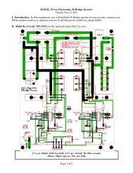
1. Convert a buck converter to a boost converter, using the circuit shown in Figure 1 of this<br />
document.<br />
2. Double-check that the polarity of your converter’s output capacitor is correct.<br />
3. Locate one of the 150W light bulb test load assemblies. Check the light bulb with an<br />
ohmmeter to make sure it is not burned out.<br />
4. Connect the light bulb test load to your circuit.<br />
5. Connect an oscilloscope Channel #1 to view V GS , and Channel #2 to view V DS . The<br />
ground clip of the Channel #2 probe should not be attached to the circuit, but instead it<br />
should be clipped back onto its own lead in-cable so that it does not dangle.<br />
Page 8 of 11
<strong>EE462L</strong>, <strong>Power</strong> <strong>Electronics</strong>, <strong>DC</strong>-<strong>DC</strong> <strong>Boost</strong> <strong>Converter</strong><br />
<strong>Version</strong> Oct. 3, 2011<br />
6. Do not connect a DBR yet. Connect a MOSFET firing circuit to your converter, using<br />
short wires, and then power-up your MOSFET firing circuit. Set the oscilloscope to<br />
trigger on Channel #1. Observe your oscilloscope to confirm that the controls are<br />
working properly.<br />
7. Raise the D potentiometer to the max, and then set the duty cycle limiter so D cannot<br />
exceed 0.8.<br />
8. Set D to the minimum setting, and F ≈ 100kHz.<br />
Important Note: the first time you energize your boost converter, feed the 120/25V<br />
transformer through a variac to the DBR, so that you can SLOWLY increase the voltage<br />
from zero and read the variac ammeter to detect short circuits before they become serious.<br />
A common problem is to have the MOSFET in backward, so that its internal antiparallel diode<br />
creates a short circuit. The ammeter on the variac is an excellent diagnostic tool. Once you are<br />
convinced that your circuit is working correctly, the variac is then optional. Remember – your<br />
boost converter requires <strong>DC</strong> input power from a DBR.<br />
Does your circuit have a short If so, do the following:<br />
1. Make sure that your MOSFET is not connected backwards.<br />
2. Observe VGS on the MOSFET as you vary D. Does the waveform look correct<br />
3. Unplug the wall wart. Does the short circuit go away If not, your MOSFET may be<br />
shorted – so, disconnect the MOSFET from the converter, and perform the voltagecontrolled<br />
resistance test on the MOSFET, or use the MOSFET tester.<br />
9. Connect a variac to a 25Vac transformer, and 25Vac transformer to a DBR. Connect the<br />
DBR to your boost converter, keeping the wires short. Then, energize the 25Vac<br />
transformer and DBR. Slowly raise the variac, checking for a short circuit, so that Vac of<br />
the transformer is approximately 27-28V.<br />
10. With F ≈ 100kHz, slowly raise D so that Vout increases in steps of about 10V up to the<br />
maximum obtained with D = 0.8 or 120V, whichever is less. Measure D, Vin, Iin, Vout,<br />
and Iout as you go. Save a screen snapshot of VDS for Vout = 100V that shows the peak<br />
value of VDS. Let the circuit run at the 100Vout condition for 1 or 2 more minutes, and<br />
then turn off your circuit.<br />
Page 9 of 11
<strong>EE462L</strong>, <strong>Power</strong> <strong>Electronics</strong>, <strong>DC</strong>-<strong>DC</strong> <strong>Boost</strong> <strong>Converter</strong><br />
<strong>Version</strong> Oct. 3, 2011<br />
Save screen<br />
snapshot #1<br />
VDS for 90kHz, 120V<br />
11. With your circuit turned off, quickly and carefully use your hand to check MOSFET<br />
heat sink temperature and any other hot components. You can also use an infrared<br />
thermometer for this step.<br />
12. Compare your measured Vout/Vin to theory. Multiply voltages and currents to compute<br />
input and output powers, and then compute the efficiency of your circuit for each Vout<br />
measured. Plot your results in your written report.<br />
13. Take can also take your solar lab data while you are doing the boost converter. Use a<br />
150W light bulb as a load. Connect a DBR between a solar panel pair and your boost<br />
converter to steady the panel current. Sweep D to find the maximum power point.<br />
Compute the maximum power point value of Rload = Vout/Iout and the corresponding<br />
equivalent max power resistance seen by the solar panels. Does the ratio of Rload<br />
resistance to equivalent resistance seem by the solar panels check with D<br />
Page 10 of 11
<strong>EE462L</strong>, <strong>Power</strong> <strong>Electronics</strong>, <strong>DC</strong>-<strong>DC</strong> <strong>Boost</strong> <strong>Converter</strong><br />
<strong>Version</strong> Oct. 3, 2011<br />
Page 11 of 11