
Create successful ePaper yourself
Turn your PDF publications into a flip-book with our unique Google optimized e-Paper software.
CML Microcircuits<br />
COMMUN<strong>IC</strong>ATION SEM<strong>IC</strong>ONDUCTORS<br />
D/869/2 July 2003<br />
<strong>CMX869</strong><br />
Low Power<br />
<strong>V.32</strong> <strong>bis</strong> <strong>Modem</strong><br />
Provisional Issue<br />
Features<br />
Applications<br />
• <strong>V.32</strong> <strong>bis</strong>/<strong>V.32</strong>/V.22 <strong>bis</strong>/V.22 automodem. (14400, • Telephone Telemetry Systems<br />
12000, 9600, 7200, 4800, 2400, 1200 bps duplex) • Remote Utility Meter Reading<br />
• V.23 (1200/75, 1200/1200, 75, 1200 bps FSK) • Security Systems<br />
• Bell 202 (1200/150, 1200/1200, 150, 1200 bps FSK) • Industrial Control Systems<br />
• V.21 or Bell 103 (300/300 bps FSK) • Electronic Cash Terminals<br />
• DTMF/Tones Transmit and Receive • Pay-Phones<br />
• ‘Powersave’ Standby Mode • Cable TV Set-Top Boxes<br />
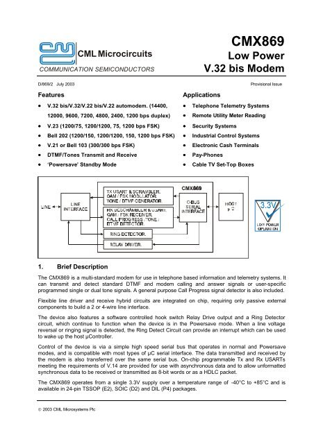
1. Brief Description<br />
The <strong>CMX869</strong> is a multi-standard modem for use in telephone based information and telemetry systems. It<br />
can transmit and detect standard DTMF and modem calling and answer signals or user-specific<br />
programmed single or dual tone signals. A general purpose Call Progress signal detector is also included.<br />
Flexible line driver and receive hybrid circuits are integrated on chip, requiring only passive external<br />
components to build a 2 or 4-wire line interface.<br />
The device also features a software controlled hook switch Relay Drive output and a Ring Detector<br />
circuit, which continue to function when the device is in the Powersave mode. When a line voltage<br />
reversal or ringing signal is detected, the Ring Detect Circuit can provide an interrupt which can be used<br />
to wake up the host µController.<br />
Control of the device is via a simple high speed serial bus that operates in normal and Powersave<br />
modes, and is compatible with most types of µC serial interface. The data transmitted and received by<br />
the modem is also transferred over the same serial bus. On-chip programmable Tx and Rx USARTs<br />
meeting the requirements of V.14 are provided for use with asynchronous data and to allow unformatted<br />
synchronous data to be received or transmitted as 8-bit words or as a HDLC packet.<br />
The <strong>CMX869</strong> operates from a single 3.3V supply over a temperature range of -40°C to +85°C and is<br />
available in 24-pin TSSOP (E2), SO<strong>IC</strong> (D2) and DIL (P4) packages.<br />
© 2003 CML Microsystems Plc
Low Power <strong>V.32</strong> <strong>bis</strong> <strong>Modem</strong><br />
<strong>CMX869</strong><br />
Section<br />
CONTENTS<br />
Page<br />
1. Brief Description..................................................................................1<br />
2. Block Diagram .....................................................................................3<br />
3. Signal List ............................................................................................4<br />
4. External Components .........................................................................6<br />
4.1 Power Supply Connections ....................................................7<br />
4.2 Ring Detector Interface...........................................................8<br />
4.3 Line Interface...........................................................................9<br />
5. General Description...........................................................................11<br />
5.1 Tx USART ..............................................................................12<br />
5.2 FSK and QAM Modulators ....................................................14<br />
5.3 Tx Filter and Equaliser..........................................................14<br />
5.4 DTMF/Tone Generator ..........................................................14<br />
5.5 Tx Level Control and Output Buffer.....................................14<br />
5.6 Rx DTMF/Tones Detectors ...................................................14<br />
5.7 Rx <strong>Modem</strong> Filterering and Demodulation ............................15<br />
5.8 Rx <strong>Modem</strong> Pattern Detectors ...............................................15<br />
5.9 Rx USART..............................................................................16<br />
6. C-BUS Interface and Software Description ......................................18<br />
6.1 General Reset Command .....................................................20<br />
6.2 General Control Register ......................................................20<br />
6.3 Transmit Mode Register .......................................................22<br />
6.4 Receive Mode Register.........................................................25<br />
6.5 QAM <strong>Modem</strong> Command Register.........................................27<br />
6.6 Tx Data Register....................................................................28<br />
6.7 Rx Data Register ...................................................................29<br />
6.8 Status Register......................................................................30<br />
6.9 QAM <strong>Modem</strong> Status Register ...............................................33<br />
6.10 Programming Register..........................................................35<br />
7. Application Notes ..............................................................................38<br />
8. Performance Specification................................................................39<br />
8.1 Electrical Performance .........................................................39<br />
8.1.2 Operating Limits .......................................................39<br />
8.1.3 Operating Characteristics ........................................40<br />
8.2 Packaging..............................................................................45<br />
© 2003 CML Microsystems Plc 2 D/869/2
Low Power <strong>V.32</strong> <strong>bis</strong> <strong>Modem</strong><br />
<strong>CMX869</strong><br />
2. Block Diagram<br />
Figure 1 Block Diagram<br />
© 2003 CML Microsystems Plc 3 D/869/2
Low Power <strong>V.32</strong> <strong>bis</strong> <strong>Modem</strong><br />
<strong>CMX869</strong><br />
3. Signal List<br />
<strong>CMX869</strong><br />
D2/E2/P4<br />
Signal<br />
Description<br />
Pin No. Name Type<br />
1 REPLY DATA TS A 3-state C-BUS serial data output to the µC. This<br />
output is high impedance when not sending data to the<br />
µC.<br />
2 RDRVN OP Relay Drive output, low resistance pull down to VSS<br />
when active and medium resistance pull up to VDD<br />
when inactive.<br />
4 SERIAL<br />
CLOCK<br />
IP The C-BUS serial clock input from the µC.<br />
5 COMMAND<br />
DATA<br />
IP<br />
The C-BUS serial data input from the µC.<br />
6 CSN IP The C-BUS chip select input from the µC.<br />
8 RXA IP The non-inverting input to the Rx Input Amplifier<br />
9 RXBN IP A second, switched inverting input to the Rx Input<br />
Amplifier. Used to increase the input stage gain. If not<br />
required, leave this pin unconnected.<br />
10 RXAN IP The inverting input to the Rx Input Amplifier<br />
11 RXAFB OP The output of the Rx Input Amplifier.<br />
13 V BIAS OP Internally generated bias voltage of approximately<br />
AV DD /2, except when the device is in ‘Powersave’<br />
mode when V BIAS will discharge to AV SS . Must be<br />
decoupled to AV SS by a capacitor mounted close to the<br />
device pins.<br />
14 TXAN OP The inverted output of the Tx Output Buffer.<br />
15 TXA OP The non-inverted output of the Tx Output Buffer.<br />
17 RDN IP Schmitt trigger input to the (inverting) Ring signal<br />
detector. Connect to DV DD if Ring Detector is not<br />
used.<br />
18 - NC Reserved for future use. Do not connect to this pin.<br />
20 V DEC PWR/<br />
OP<br />
Internally generated 2.5V supply voltage. Must be<br />
decoupled to DV SS by capacitors mounted close to the<br />
device pins. No other connections allowed.<br />
21 XTAL/CLOCK IP The input to the oscillator inverter from the Xtal circuit<br />
or external clock source.<br />
22 XTALN OP The output of the on-chip Xtal oscillator inverter.<br />
24 IRQN OP A ‘wire-ORable’ output for connection to a µC Interrupt<br />
Request input. This output is pulled down to DVSS<br />
when active and is high impedance when inactive. An<br />
external pullup resistor is required ie R1 of Figure 2<br />
© 2003 CML Microsystems Plc 4 D/869/2
Low Power <strong>V.32</strong> <strong>bis</strong> <strong>Modem</strong><br />
<strong>CMX869</strong><br />
Signal list (cont.)<br />
<strong>CMX869</strong> E2 Signal Description<br />
Pin No. Name Type<br />
3, 19 DV SS PWR The negative supply rail (ground) for the digital on-chip<br />
circuits.<br />
7, 16 AV SS PWR The negative supply rail (ground) for the analogue onchip<br />
circuits.<br />
12 AV DD PWR The positive supply rail for the analogue on-chip<br />
circuits. Levels and thresholds within the device are<br />
proportional to this voltage.<br />
23 DV DD PWR The positive supply rail for the digital on-chip circuits.<br />
Notes: IP = Input<br />
OP = Output<br />
TS = 3-state Output<br />
PWR = Power<br />
NC = No Connection<br />
© 2003 CML Microsystems Plc 5 D/869/2
Low Power <strong>V.32</strong> <strong>bis</strong> <strong>Modem</strong><br />
<strong>CMX869</strong><br />
4. External Components<br />
R1 100kΩ C2, C4, C7, C9 100nF<br />
X1 6.144MHz C5, C6 47pF (see text)<br />
C1, C3, C8 10uF<br />
Resistors ±5%, capacitors ±20% unless otherwise stated.<br />
Figure 2a Recommended External Components for a Typical Application<br />
This device is capable of detecting and decoding small amplitude signals. To achieve this DV DD , AV DD<br />
and V BIAS should be decoupled and the receive path protected from extraneous in-band signals. It is<br />
recommended that the printed circuit board is laid out with both AV SS and DV SS ground planes in the<br />
<strong>CMX869</strong> area, as shown in Figure 2b, with provision to make a link between them close to the <strong>CMX869</strong>.<br />
To provide a low impedance connection to ground, the decoupling capacitors (C1 – C4, C7, C8) must be<br />
mounted as close to the <strong>CMX869</strong> as possible and connected directly to their respective ground plane.<br />
This will be achieved more easily by using surface mounted capacitors.<br />
V BIAS is used as an internal reference for detecting and generating the various analogue signals. It must<br />
be carefully decoupled, to ensure its integrity. If V BIAS needs to be used (other than as shown in figures<br />
4a or 4b) to set external analogue levels, it must be buffered with a high input impedance buffer.<br />
The values for capacitors C5 and C6 are suggestions for use with many typical crystals. However the<br />
values of these capacitors must be chosen to comply with the crystal manufacturer’s specification, to<br />
ensure that the clock accuracy is within 100ppm. The DV SS connections to the Xtal oscillator capacitors<br />
C5 and C6 should also be of low impedance and preferably be part of the DV SS ground plane to ensure<br />
reliable start up of the oscillator.<br />
© 2003 CML Microsystems Plc 6 D/869/2
Low Power <strong>V.32</strong> <strong>bis</strong> <strong>Modem</strong><br />
<strong>CMX869</strong><br />
4.1 Power Supply Connections<br />
ANALOGUE<br />
DIGITAL<br />
C2, C9 100nF C4, C7 100nF<br />
C1 10uF C3, C8 10uF<br />
L2 100nH (optional) L1 100nH (optional)<br />
Figure 2b Recommended Power Supply Connections and De-coupling<br />
The inductors L1 and L2 can be omitted but this may degrade system performance.<br />
Ensure that the length of the tracks between capacitors C2, C4, C7 and C9 and their corresponding<br />
<strong>CMX869</strong> device pins (pins 12, 23, 20 and 13) are kept as short as possible.<br />
© 2003 CML Microsystems Plc 7 D/869/2
Low Power <strong>V.32</strong> <strong>bis</strong> <strong>Modem</strong><br />
<strong>CMX869</strong><br />
4.2 Ring Detector Interface<br />
R20 10kΩ, 0.5W C21 0.33µF<br />
R21 470kΩ D1, D2 18V zener<br />
R22 100Ω D3 Opto isolator (NEC PS2701-1)<br />
C20 0.33µF, 250V D4 1N4004<br />
Resistors ±5%, capacitors ±20%. Circuit and all component types and values TBD.<br />
Figure 3 Ring Signal Detector Interface Circuit<br />
Figure 3 shows how the <strong>CMX869</strong> may be used to detect the large amplitude Ringing signal voltage<br />
present on the 2-wire line at the start of an incoming telephone call. The ring signal is usually applied at<br />
the subscriber's exchange as an ac voltage inserted in series with one of the telephone wires and will<br />
pass through C20, R20, D1 and D2, and appear at the terminals of D3. When the signal reaches the<br />
zeners’ (D1, D2) turn-on voltage, current will flow into the opto-isolator diode, turning on its output<br />
transistor and discharging capacitor C21. Resistor R22 limits the current drawn by the opto-isolator<br />
output to ~30mA peak (TBD). Whilst the ring tone is active and exceeds the zener voltage, the RDN node<br />
will be taken low and the output of the Schmitt trigger will go high. The state of bit 14 (Ring Detect) of the<br />
Status Register directly corresponds to the state of the Ring Detect Schmitt trigger output. If the<br />
corresponding interrupt mask bit is set to 1, a C-BUS interrupt will be initiated (see the Status Register<br />
description in section 6.8).<br />
The minimum amplitude ringing signal that is certain to be detected is: Vzener + 2xVdiode + 2V (TBD).<br />
© 2003 CML Microsystems Plc 8 D/869/2
Low Power <strong>V.32</strong> <strong>bis</strong> <strong>Modem</strong><br />
<strong>CMX869</strong><br />
4.3 Line Interface<br />
A line interface circuit is needed to provide dc isolation and to terminate the line. The <strong>CMX869</strong> is<br />
connected to the line when the line relay is closed. The relay may be driven from the RDRVN output, as<br />
shown in figure 4a. Control of the output level of the RDRVN pin is described in section 6.2. The diagrams<br />
of Figure 4a and Figure 4b are functional representations only and should not be used in product designs.<br />
A reference design will be available separately.<br />
2-Wire Line Interface<br />
Figure 4a shows a simplified interface for use with a 600Ω 2-wire line. The line termination impedance is<br />
provided by the transformer, R13 and C10, high frequency noise is attenuated by C10 and C11, while<br />
R11 and R12 set the receive signal level into the modem. For clarity the 2-wire line protection circuits<br />
have not been shown.<br />
R11 130kΩ (see text) C3 See Figure 2<br />
R12 100kΩ C10 33nF<br />
R13 600Ω C11 100pF<br />
R14 15kΩ (see text) C12 100nF, 250V (see text)<br />
Resistors ±5%, capacitors ±20%<br />
Figure 4a 2-Wire Line Interface Circuit<br />
The transmit line signal level is determined by the voltage swing between the TXA and TXAN pins, less<br />
6dB due to the line termination resistor R13, and less the loss in the line coupling transformer. Allowing<br />
for 1dB loss in the transformer, with the Tx Mode Register set for a Tx Level Control gain of 0dB the<br />
nominal transmit line levels will be:<br />
QAM and FSK Tx modes (no guard tone)<br />
Single tone transmit mode<br />
DTMF transmit mode<br />
VDD = 3.3V<br />
-7.5 dBm<br />
-7.5 dBm<br />
-3.5 and -5.5 dBm<br />
For a line impedance of 600Ω, 0dBm = 775mVrms. See also section 8.1.3<br />
© 2003 CML Microsystems Plc 9 D/869/2
Low Power <strong>V.32</strong> <strong>bis</strong> <strong>Modem</strong><br />
<strong>CMX869</strong><br />
In the receive direction, the signal detection thresholds within the <strong>CMX869</strong> are proportional to AVDD and<br />
are affected by the Rx Gain Control gain setting in the Rx Mode Register. The signal level into the<br />
<strong>CMX869</strong> is affected by the line coupling transformer loss and the values of R11 and R12 of Figure 4a.<br />
The value of R11 should be chosen so that the received signal level at the RXAFB pin is 3.6dB lower<br />
than that on the 2-wire line. For example if the transformer loss is 1dB then R11 should be 130kΩ. The<br />
value of R14 (15kΩ) is chosen to apply approximately 20dB of extra gain, when required by Type 1 Caller<br />
Line Identification.<br />
For best Rx performance, it is recommended that the transformer coupling arrangement should provide at<br />
least 7dB trans-hybrid loss.<br />
The RXBN input can be selected by setting bit 14 of the General Control Register to 1, which internally<br />
connects RXBN to RXAN. With the components shown in Figures 4a and 4b, this will add approximately<br />
20dB to the Rx gain, by connecting R14 in parallel with R11. This facilitates detection of certain signals<br />
whilst on-hook, such as may be required for Type 1 Caller Line Identification reception. For the 2-wire<br />
line interface shown in Figure 4a, capacitor C12 is required to provide an AC path through to the device<br />
when the relay is open. If this facility is not required, R14 and C12 can be omitted.<br />
4-Wire Line Interface<br />
Figure 4b shows a simplified interface for use with a 600Ω 4-wire line. The line terminations are provided<br />
by R10 and R13, high frequency noise is attenuated by C11 while R11 and R12 set the receive signal<br />
level into the modem. Transmit and receive line level settings and the values of R11 and R14 are as for<br />
the 2-wire circuit.<br />
R10, 13 600Ω C3 See Figure 2<br />
R11 130kΩ (see text) C11 100pF<br />
R12 100kΩ C12 33nF<br />
R14 15kΩ (see text)<br />
Resistors ±5%, capacitors ±20%<br />
Figure 4b 4-Wire Line Interface Circuit<br />
© 2003 CML Microsystems Plc 10 D/869/2
Low Power <strong>V.32</strong> <strong>bis</strong> <strong>Modem</strong><br />
<strong>CMX869</strong><br />
5. General Description<br />
The <strong>CMX869</strong> can operate as a full duplex QAM (Quadrature Amplitude Modulation) or DPSK (Differential<br />
Phase Shift Keying) automodem, using the following modulation schemes:<br />
• <strong>V.32</strong><strong>bis</strong><br />
• <strong>V.32</strong><br />
• V.22<strong>bis</strong><br />
• V.22<br />
with data rates of 14400, 12000, 9600, 7200, 4800, 2400 or 1200bps.<br />
Note: reference to QAM elsewhere in the datasheet implies QAM or DPSK, according to selected<br />
operating mode.<br />
It can also be set to operate in the following low speed modem modes:<br />
• V.21 or Bell 103. 300/300bps duplex FSK (Frequency Shift Keying).<br />
• V.23 modem. 1200 or 75 bps FSK.<br />
• Bell 202 modem. 1200 or 150 bps FSK.<br />
The transmit circuits can also be set to any one of the following:<br />
• DTMF transmit.<br />
• Single tone transmit (from a range of modem calling, answer and other tone frequencies)<br />
• User programmed tone or tone pair transmit (programmable frequencies and levels)<br />
• Disabled.<br />
And the receive circuits can be set to:<br />
• DTMF detect.<br />
• 2100Hz and 2225Hz answer tone detect.<br />
• Call progress signal detect.<br />
• User programmed tone or tone pair detect.<br />
• Disabled.<br />
The Ring Detect, Tone Decoder and FSK modem circuits can be configured to facilitate Type 1 (On-<br />
Hook) Caller Identification. This facility is the subject of separate application notes.<br />
When not in use, the <strong>CMX869</strong> may be set into a Powersave mode, which disables all circuitry except for<br />
the on-chip regulator, the C-BUS interface and the Ring Detector.<br />
© 2003 CML Microsystems Plc 11 D/869/2
Low Power <strong>V.32</strong> <strong>bis</strong> <strong>Modem</strong><br />
<strong>CMX869</strong><br />
5.1 Tx USART<br />
A flexible Tx USART is provided for all modem modes, meeting the requirements of V.14 for the QAM<br />
(<strong>V.32</strong><strong>bis</strong>/<strong>V.32</strong>/V.22<strong>bis</strong>/V.22) modem modes.<br />
It can be programmed to transmit continuous patterns, Start-Stop characters, Synchronous unformatted<br />
data or HDLC formatted packets.<br />
In HDLC, Synchronous Data and Start-Stop modes the data to be transmitted is written by the µC into the<br />
C-BUS Tx Data Register. The Tx (and Rx) Data Register can be set to operate in 8 or 16-bit mode by<br />
setting the General Control Register b10 appropriately.<br />
In 16-bit (2 character) mode data written to the Tx Data Register at C-BUS address $E3 will be treated<br />
as two octets, b15-8 which will be transmitted first and b7-0 which will be transmitted second. If there is a<br />
need to transmit a single octet when the Tx Data Register has been set to 16-bit mode this can be<br />
achieved by writing the 8-bit data to C-BUS address $E4 instead of $E3.<br />
If the Tx Data Register has been set to operate in 8-bit (1 character) mode, data should normally be<br />
written to C-BUS address $E3, address $E4 being used to provide for Start-Stop transmit data<br />
overspeed as described later.<br />
If Synchronous Data mode has been selected the 8 data bits of each octet in the Tx Data Buffer are<br />
transmitted serially, the lsb being sent first.<br />
In Start-Stop mode an asynchronous character is transmitted for each octet in the Tx Data Register.<br />
Each character consists of a single Start bit followed by 5, 6, 7 or 8 data bits from the Tx Data Buffer -<br />
lsb first - followed by an optional Parity bit then - normally - one or two Stop bits. The Start, Parity and<br />
Stop bits are generated by the USART as determined by the Tx Mode Register settings and are not taken<br />
from the Tx Data Register.<br />
In HDLC mode the octets from the Tx Data Register are packetized into a HDLC Frame consisting of a<br />
Flag byte (01111110 binary) followed by the data octets themselves, each transmitted lsb first, followed<br />
by a 16-bit Frame Check Sequence followed by another Flag byte to mark the end of the Frame. To<br />
prevent the data or FCS aliasing a Flag byte a binary 0 is inserted in the transmit bit stream after every 5<br />
consecutive 1s in the data and FCS fields. The Flag bytes and FCS are automatically generated by the<br />
<strong>CMX869</strong>.<br />
Figure 5a Tx USART (in 16 Bit Mode)<br />
© 2003 CML Microsystems Plc 12 D/869/2
Low Power <strong>V.32</strong> <strong>bis</strong> <strong>Modem</strong><br />
<strong>CMX869</strong><br />
Figure 5b Tx USART Output: Start-Stop mode, 8 Data Bits + Parity<br />
Figure 5c HDLC Frame Structure<br />
Every time the contents of the C-BUS Tx Data Register have been transferred to the Tx Data Buffer the<br />
Tx Data Ready flag bit of the Status Register is set to 1 to indicate that new data should be loaded into<br />
the C-BUS Tx Data Register. This flag bit will be cleared to 0 when a new value is loaded into the Tx Data<br />
Register.<br />
If a new value is not loaded into the Tx Data Register in time for the next Tx Data Register to Tx Data<br />
Buffer transfer then the Status Register Tx Data Underflow bit will be set to 1. This bit will be cleared to 0<br />
when a new value is loaded into the Tx Data Register<br />
In Synchronous Data mode the last transmitted byte will be re-transmitted if there is no new data in the<br />
Transmit Data Register. In Start-Stop mode a continuous Stop signal (1) will be transmitted.<br />
In HDLC mode the Status Register Tx Data Underflow bit becoming set to 1 is taken by the <strong>CMX869</strong> to<br />
indicate the end of data for a frame. The <strong>CMX869</strong> will then transmit the FCS followed by at least one Flag<br />
byte. Flag bytes will continue to be transmitted until a new Frame is started by loading a new value into<br />
the Transmit Data Register.<br />
In all modes the transmitted bit and baud rates are the nominal rates for the selected modem type, with an<br />
accuracy determined by the XTAL frequency accuracy, however for QAM modes V.14 requires that Start-<br />
Stop characters can be transmitted at up to 1% overspeed (basic signalling rate range) or 2.3%<br />
overspeed (extended signalling rate range) by deleting a Stop bit from no more than one out of every 8<br />
(basic range) or 4 (extended range) consecutive transmitted characters.<br />
To accommodate this V.14 requirement the <strong>CMX869</strong> allows the controlling µC to reduce the number of<br />
transmitted Stop bits by one for selected characters in QAM Start-Stop modes. To do this, the device<br />
must be set to operate in 1 character mode for the entire transmission, by clearing General Control<br />
Register b10 to 0. Characters written to thc C-BUS Tx Data Register at address $E3 will then be<br />
transmitted with the programmed number of Stop bits, but a character written to $E4 will be transmitted<br />
with one less Stop bit than the number programmed in the Tx Mode Register.<br />
In FSK Start-Stop modes, if the device is set for 1 character mode (General Control Register b10 = 0)<br />
data written to $E4 will be transmitted with a 12.5% reduction in the length of the Stop bit at the end of<br />
that character. In all 8 bit Synchronous Data modes data, written to $E4 will be treated as though it had<br />
been written to $E3. The behaviour is not defined for 16 bit data mode.<br />
The underspeed transmission requirement of V.14 is automatically met by the <strong>CMX869</strong> as in Start-Stop<br />
mode it will insert extra Stop bit(s) if it has to wait for new data to be loaded into the C-BUS Tx Data<br />
Register.<br />
The QAM (<strong>V.32</strong><strong>bis</strong>/<strong>V.32</strong>/V.22<strong>bis</strong>/V.22) modulators include compatible data scrambler functions that are<br />
automatically enabled as required.<br />
© 2003 CML Microsystems Plc 13 D/869/2
Low Power <strong>V.32</strong> <strong>bis</strong> <strong>Modem</strong><br />
<strong>CMX869</strong><br />
5.2 FSK and QAM Modulators<br />
Serial data from the USART is fed to the FSK modulator if V.21, V.23, Bell 103 or Bell 202 mode has<br />
been selected, or to the QAM modulator for V.22<strong>bis</strong>, V.22, <strong>V.32</strong><strong>bis</strong> and <strong>V.32</strong> modes.<br />
The FSK modulator generates one of two frequencies according to the transmit mode and the value of<br />
current transmit data bit.<br />
In V.22<strong>bis</strong> and V.22 modes, QAM modulation is applied to a carrier of 1200Hz (Low Band, Calling modem)<br />
or 2400Hz (High Band, Answering modem).<br />
In <strong>V.32</strong><strong>bis</strong> and <strong>V.32</strong> modes, QAM modulation is applied to a carrier of 1800Hz, using Trellis encoding for<br />
most bit rates.<br />
5.3 Tx Filter and Equaliser<br />
The FSK or QAM modulator output signal is fed through the Transmit Filter and Equaliser block which<br />
limits the out-of-band signal energy to acceptable limits. The appropriate equalisation for the particular<br />
operating mode is determined and selected automatically, by the device.<br />
5.4 DTMF/Tone Generator<br />
In DTMF/Tones mode this block generates DTMF signals or single or dual frequency tones. In V.22 <strong>bis</strong><br />
modem mode it is used to generate the optional 550Hz or 1800Hz guard tone.<br />
5.5 Tx Level Control and Output Buffer<br />
The outputs (if present) of the Transmit Filter and DTMF/Tone Generator are summed then passed<br />
through the programmable Tx Level Control and Tx Output Buffer to the pins TXA and TXAN. The Tx<br />
Output Buffer has symmetrical outputs to provide sufficient line voltage swing and to reduce harmonic<br />
distortion of the signal.<br />
In normal (non loopback) mode, the output from the Rx Input Amplifier is fed to the Rx Gain Control block.<br />
This provides the ability to attenuate the received signal by up to 10.5dB, depending on the value<br />
programmed into the Receive Mode Register. The output from the Rx Gain Control block is routed either<br />
to the <strong>Modem</strong> functions or to the Tone Detectors.<br />
5.6 Rx DTMF/Tones Detectors<br />
In Rx Tones Detect mode the received signal, after passing through the Rx Gain Control block, is fed to<br />
the DTMF / Tones / Call Progress / Answer Tone Detector. The user may select any of four separate<br />
detectors:<br />
The DTMF Detector detects standard DTMF signals and identifies the transmitted character in the Status<br />
Register. A valid DTMF signal will set bit 5 of the Status Register to 1 for as long as the signal is<br />
detected.<br />
The Programmable Tone Pair Detector includes two separate tone detectors (see Figure 10). The first<br />
detector will set bit 6 of the Status Register for as long as a valid signal is detected, the second detector<br />
sets bit 7, and bit 10 of the Status Register will be set when both tones are detected.<br />
© 2003 CML Microsystems Plc 14 D/869/2
Low Power <strong>V.32</strong> <strong>bis</strong> <strong>Modem</strong><br />
<strong>CMX869</strong><br />
The Call Progress Detector measures the amplitude of the signal at the output of a 275Hz - 665Hz<br />
bandpass filter and sets bit 10 of the Status Register to 1 when the signal level exceeds the<br />
measurement threshold. The response of the Call Progress filter, including the effect of external<br />
components of figures 4a and 4b, is shown in Figure 6.<br />
10<br />
0<br />
-10<br />
dB<br />
-20<br />
-30<br />
-40<br />
-50<br />
-60<br />
0 0.5 1 1.5 2 2.5 3 3.5 4<br />
kHz<br />
Figure 6 Response of Call Progress Filter<br />
The Answer Tone Detector measures both amplitude and frequency of the received signal and sets bit 6<br />
or bit 7 of the Status Register when a valid 2225Hz or 2100Hz signal is received.<br />
5.7 Rx <strong>Modem</strong> Filterering and Demodulation<br />
When the receive part of the <strong>CMX869</strong> is operating as a modem, the received signal is fed through a<br />
bandpass filter to attenuate unwanted signals. The characteristics of the filter are determined by the<br />
chosen receive modem type and frequency band.<br />
The output of the filter is fed to the appropriate FSK or QAM demodulator depending on the selected<br />
modem type.<br />
In FSK modem modes the signal level at the output of the Filter is also measured, compared to a<br />
threshold value, and the result controls bit 10 of the Status Register.<br />
In QAM modem modes, a <strong>V.32</strong> <strong>bis</strong>/<strong>V.32</strong> echo canceller is included, which will work with a round trip delay<br />
of up to 1.25seconds.<br />
5.8 Rx <strong>Modem</strong> Pattern Detectors<br />
In FSK modem modes the received bit stream is monitored for continuous 1’s, for continuous 0’s, and for<br />
continuous alternating 1’s and 0’s. Bit 7, 8 or 9 of the Status Register will be set to 1 whenever 32 bits of<br />
the appropriate pattern has been received and will then remain at 1 for 12 bit times after the end of the<br />
detected pattern unless the receive operating mode is changed, in which case the pattern detectors are<br />
reset within 2 msec.<br />
In QAM modem modes a V.14 ‘Break’ signal detector is implemented in Start-Stop mode by monitoring<br />
the received data and setting bit 8 of the Status Register when 2N + 4 consecutive 0’s have been<br />
received, N being the total number of bits per character including the Start, Stop and any Parity bits.<br />
The demodulated data is passed through a de-scrambler according to the requirements of the receiver<br />
operating mode. This function is enabled automatically, as required.<br />
© 2003 CML Microsystems Plc 15 D/869/2
Low Power <strong>V.32</strong> <strong>bis</strong> <strong>Modem</strong><br />
<strong>CMX869</strong><br />
5.9 Rx USART<br />
A flexible Rx USART is provided for all modem modes, meeting the requirements of V.14 for QAM (V.22,<br />
V.22 <strong>bis</strong>, <strong>V.32</strong> and <strong>V.32</strong> <strong>bis</strong>) modem modes. Depending on the setting of the Rx Mode Register it will treat<br />
the received data bit stream as Synchronous data, as Start-Stop characters or as HDLC Frames.<br />
Synchronous mode<br />
In Synchronous mode the received data bits are all fed into an internal Rx Data Buffer which is copied<br />
into the C-BUS Rx Data Register after every 8 or 16 bits, depending on the setting of the General Control<br />
Register ‘2 character mode’ bit, b10.<br />
Start-Stop (asynchronous) mode<br />
In Start-Stop mode the USART Control logic looks for the start of each character, then feeds only the<br />
required number of data bits (not parity) into an internal Rx Data Buffer. If the parity bit is used, both<br />
parity and the presence of a Stop bit are checked. Depending on the setting of b10 of the General<br />
Control Register, the data bits from 1 or 2 received characters are placed into the C-BUS Rx Data<br />
Register. If parity has been enabled the C-BUS Status Register ‘Even Parity’ bit(s) are set or cleared<br />
according to the received parity.<br />
If the Stop bit is missing at the end of a character (a ‘0’ received instead of a ‘1’) the received character<br />
will still be placed into the C-BUS Rx Data Register, but unless allowed by the V.14 overspeed option<br />
described below, the Status Register Rx Framing Error bit will be set to ‘1’ and the USART will resynchronise<br />
onto the next ‘1’ – ‘0’ (Stop – Start) transition.<br />
If 2-character mode has been selected, received characters will normally be transferred to the C-BUS Rx<br />
Data Register two at a time and the Status Register b1 set to 1. However, the USART includes a time-out<br />
function so that if a message contains an odd number of characters the final character will be transferred<br />
to the Rx Data Register and b1 of the Status Register will be cleared to ‘0’. This indicates that the next<br />
data to be read from the Rx Data Register holds the single last character in the most significant byte.<br />
Figure 7 Rx USART (in 16 Bit Mode)<br />
© 2003 CML Microsystems Plc 16 D/869/2
Low Power <strong>V.32</strong> <strong>bis</strong> <strong>Modem</strong><br />
<strong>CMX869</strong><br />
HDLC mode<br />
In HDLC mode the <strong>CMX869</strong> recognises the start and end of an HDLC Frame by monitoring the received<br />
bit stream for the presence of the flag byte (01111110 binary). The received data and FCS octets within<br />
the Frame are then passed to the C-BUS Rx Data Register (one or two octets at a time depending on the<br />
setting of the ’2-character’ bit) after removal of any ‘stuffed’ 0’s. A 16-bit Frame Check Sequence is<br />
calculated from the received data octets and compared to the received FCS at the end of the Frame, bit<br />
4 of the Status Register being set to 1 if the two FCSs do not match.<br />
If 2-character mode has been selected, received data and FCS octets will normally be transferred to the<br />
C-BUS Rx Data Register two at a time, and Status Register bit 1 will be set to 1. However if the message<br />
contains an odd number of octets, Status Register bit 1 will be cleared to 0 when the final octet is<br />
transferred to the Rx Data Register. This indicates that the next data to be read from the Rx Data<br />
Register holds the single last character in the most significant byte.<br />
Status Register Rx Data Ready and Rx Data Overflow bits<br />
Whenever a new character or characters is copied into the C-BUS Rx Data Register, the Rx Data Ready<br />
flag bit b6 of the Status Register is set to ‘1’ to prompt the µC to read the new data.<br />
If the µC has not read the previous data from the Rx Data Register by the time that the <strong>CMX869</strong> places<br />
fresh data into it, the Rx Data Overflow flag bit, b5 of the Status Register, will be set to 1.<br />
The Rx Data Ready flag and Rx Data Overflow bits are cleared to 0 when the Rx Data Register is read<br />
by the µC.<br />
Overspeed<br />
For QAM (V.22, V.22 <strong>bis</strong>, <strong>V.32</strong> and <strong>V.32</strong> <strong>bis</strong>) Start-Stop modes, V.14 requires that the receive USART be<br />
able to cope with missing Stop bits; up to 1 missing Stop bit in every 8 consecutive received characters<br />
being allowed for the +1% overspeed (basic signalling rate) V.14 mode and 1 in 4 for the +2.3%<br />
overspeed (extended signalling rate) mode.<br />
To accommodate the requirements of V.14, the <strong>CMX869</strong> Rx Mode Register can be set for 0, +1% or<br />
+2.3% overspeed operation in QAM modes. Missing Stop bits beyond those allowed by the selected<br />
overspeed option will set the Rx Framing Error flag bit of the Status Register.<br />
© 2003 CML Microsystems Plc 17 D/869/2
Low Power <strong>V.32</strong> <strong>bis</strong> <strong>Modem</strong><br />
<strong>CMX869</strong><br />
6. C-BUS Interface and Software Description<br />
This block provides for the transfer of data and control or status information between the <strong>CMX869</strong>’s<br />
internal registers and the µC over the C-BUS serial bus. Each transaction consists of a single Register<br />
Address byte sent from the µC which may be followed by one or more data bytes sent from the µC to be<br />
written into one of the <strong>CMX869</strong>’s Write Only Registers, or one or more bytes of data read out from one<br />
of the <strong>CMX869</strong>’s Read Only Registers, as illustrated in Figure 8.<br />
Data sent from the µC on the Command Data line is clocked into the <strong>CMX869</strong> on the rising edge of the<br />
Serial Clock input. Reply Data sent from the <strong>CMX869</strong> to the µC is valid when the Serial Clock is high. The<br />
CSN line must be held low during a data transfer and kept high between transfers. The C-BUS interface is<br />
compatible with most common µC serial interfaces and may also be easily implemented with general<br />
purpose µC I/O pins controlled by a simple software routine. Figure 13 gives detailed C-BUS timing<br />
requirements.<br />
The following C-BUS addresses and registers are used by the <strong>CMX869</strong>:<br />
General Reset Command (address only, no data). Address $01<br />
General Control Register, 16-bit write only. Address $E0<br />
Transmit Mode Register, 16-bit write-only. Address $E1<br />
Receive Mode Register, 16-bit write-only. Address $E2<br />
Transmit Data Register, 8 or 16-bit write only. Address $E3<br />
Alternate Transmit Data Register, 8-bit write only. Address $E4<br />
Receive Data Register, 8 or 16-bit read-only. Address $E5<br />
Status Register, 16-bit read-only. Address $E6<br />
Programming Register, 16-bit write-only. Address $E8<br />
QAM <strong>Modem</strong> Command Register, 16-bit write-only. Address $EA<br />
QAM <strong>Modem</strong> Status Register, 16-bit read-only. Address $EB<br />
Note: The C-BUS addresses $E7, $E9, $EC, $ED, $EE and $EF are allocated for production testing and<br />
should not be accessed in normal operation.<br />
Interrupt Operation<br />
The <strong>CMX869</strong> will issue an interrupt, by taking the IRQN line low, when the IRQ bit 15 of the Status<br />
Register and the IRQ Enable bit 6 in the General Control Register are both set = 1. The IRQ bit operation<br />
is described in section 6.8.<br />
© 2003 CML Microsystems Plc 18 D/869/2
Low Power <strong>V.32</strong> <strong>bis</strong> <strong>Modem</strong><br />
<strong>CMX869</strong><br />
Figure 8 C-BUS Transactions<br />
© 2003 CML Microsystems Plc 19 D/869/2
Low Power <strong>V.32</strong> <strong>bis</strong> <strong>Modem</strong><br />
<strong>CMX869</strong><br />
6.1 General Reset Command<br />
General Reset Command (no data) C-BUS address $01<br />
This command resets the device and clears all bits of the General Control, Transmit Mode and Receive<br />
Mode Registers and bits 15 and 13-0 of the Status Register. The General Reset command places the<br />
device into Powersave mode.<br />
Whenever power is applied to the <strong>CMX869</strong>, a built in power-on-reset circuit ensures that the device<br />
powers up into the same state as follows a General Reset command. Nevertheless it is recommended<br />
that a General Reset command be sent to the device on power-up, after which the General Control<br />
Register should be set as required.<br />
6.2 General Control Register<br />
General Control Register: 16-bit write-only. C-BUS address $E0<br />
This register controls general features of the <strong>CMX869</strong> such as the Powersave and Loopback modes, the<br />
IRQ mask bits and the Relay Drive output.<br />
All bits of this register are cleared to 0 by a General Reset command.<br />
Bit: 15 14 13 12 11 10 9 8 7 6 5 4 3 2 1 0<br />
0 Hi<br />
Gain<br />
0 0 LB 2C Rly<br />
drv<br />
Pwr Rst Irqn<br />
en<br />
General Control Register b15: Reserved, set to 0<br />
IRQ Mask Bits<br />
General Control Register b14: Select high input gain<br />
This bit selects the RXBN input pin and is used to increase the input stage gain.<br />
B14 = 1 RXBN internally connected to RXAN<br />
B14 = 0 RXBN open circuit<br />
General Control Register b13,12: Reserved, set to 00<br />
General Control Register b11: Analogue Loopback test mode<br />
This bit controls the analogue loopback test mode. In loopback test mode both Transmit and<br />
Receive Mode Registers should be set to the same modem type, band and bit rate. The line<br />
interface relay must be open, as the test transmission that is fed back into the Rx path will<br />
appear at the Tx pins.<br />
b11 = 1 Local analogue loopback mode enabled<br />
b11 = 0 No loopback (normal modem operation)<br />
General Control Register b10: <strong>Modem</strong> 2-Character mode<br />
Selects whether the Tx Data and Rx Data Registers operate in 1 or 2 character mode.<br />
b10 = 1 2 character mode<br />
b10 = 0 1 character mode<br />
The character mode is only updated on exit from General Control initated reset, so General<br />
Control Register b7 must be set (written = 1) then cleared (written = 0), in conjunction with setting<br />
the desired character mode.<br />
© 2003 CML Microsystems Plc 20 D/869/2
Low Power <strong>V.32</strong> <strong>bis</strong> <strong>Modem</strong><br />
<strong>CMX869</strong><br />
General Control Register b9: Relay Drive<br />
This bit directly controls the RDRVN output pin.<br />
b9 = 1 RDRVN output pin pulled to VSS<br />
b9 = 0 RDRVN output pin pulled to VDD<br />
General Control Register b8: Power-up<br />
This bit controls the internal power supply to most of the internal circuits, including the Xtal<br />
oscillator, internal clock synthesizer and VBIAS supply. Note that the General Reset command<br />
clears this bit, putting the device into Powersave mode.<br />
b8 = 1 Device powered up normally<br />
b8 = 0 Powersave mode (all circuits disabled, except the on-chip regulator,<br />
Ring Detect, RDRVN and C-BUS interface)<br />
When power is first applied to the device, the following power-up procedure should be followed<br />
to ensure correct operation.<br />
i. (Power is applied to the device)<br />
ii. Issue a General Reset command.<br />
iii. Write to the General Control Register (address $E0 setting both the Power-up bit<br />
(b8) and the reset bit (b7) to 1 – leave in this state for a minimum of about 20ms –<br />
this is required to ensure that the crystal oscillator, on-chip regulator and the V BIAS<br />
supply are all operating prior to running any transmit or receive functions<br />
iv. The device is now ready to be programmed as and when required. Examples:<br />
• A General Reset command could be issued to clear all the registers and<br />
therefore powersave the device.<br />
• The Reset bit in the General Control Register could be set to 0 as part of a<br />
routine to program all the relevant registers for setting up a particular operating<br />
mode.<br />
When the device is switched from Powersave mode to normal operation by setting the Powerup<br />
bit to 1, the Reset bit should also be set to 1 and should be held at 1 for about 20ms while<br />
the on-chip regulator, crystal oscillator, clock synthesizer and V BIAS stabilise before starting to<br />
use the transmitter or receiver.<br />
General Control Register b7: Reset<br />
Setting this bit to 1 resets the <strong>CMX869</strong>’s internal circuitry, clearing all bits of the Transmit and<br />
Receive Mode Registers and b13-0 of the Status Register.<br />
b7 = 1 Internal circuitry in a reset condition.<br />
b7 = 0 Normal operation<br />
General Control Register b6: IRQNEN (IRQN O/P Enable)<br />
Setting this bit to 1 enables the IRQN output pin.<br />
b6 = 1 IRQN pin driven low (to VSS) if the IRQ bit of the Status Register = 1<br />
b6 = 0 IRQN pin disabled (high impedance)<br />
General Control Register b5-0: IRQ Mask bits<br />
These bits affect the operation of the IRQ bit of the Status Register as described in section 6.8<br />
© 2003 CML Microsystems Plc 21 D/869/2
Low Power <strong>V.32</strong> <strong>bis</strong> <strong>Modem</strong><br />
<strong>CMX869</strong><br />
6.3 Transmit Mode Register<br />
Transmit Mode Register: 16-bit write-only. C-BUS address $E1<br />
This register controls the <strong>CMX869</strong> transmit signal type and level. All bits of this register are cleared to 0<br />
by a General Reset command or when b7 (Reset) of the General Control Register is 1.<br />
Bit: 15 14 13 12 11 10 9 8 7 6 5 4 3 2 1 0<br />
Tx mode = modem Tx level Guard tone 00 Start-stop /<br />
synch data<br />
# data bits /<br />
synch data source<br />
Tx mode = DTMF/Tones Tx level 0 DTMF twist DTMF or Tone select<br />
Tx mode = Disabled Set to 0000 0000 0000<br />
Tx Mode Register b15-12: Tx mode<br />
These 4 bits select the transmit operating mode.<br />
b15 b14 b13 b12<br />
1 1 1 x Reserved, do not use<br />
1 1 0 1 Reserved, do not use<br />
1 1 0 0 V.22, V.22 <strong>bis</strong>, <strong>V.32</strong>, <strong>V.32</strong> <strong>bis</strong> QAM modem<br />
1 0 1 x Reserved, do not use<br />
1 0 0 1 V.21 300 bps FSK High band (Answering modem)<br />
1 0 0 0 “ Low band (Calling modem)<br />
0 1 1 1 Bell 103 300 bps FSK High band (Answering modem)<br />
0 1 1 0 “ Low band (Calling modem)<br />
0 1 0 1 V.23 FSK 1200 bps<br />
0 1 0 0 “ 75 bps<br />
0 0 1 1 Bell 202 FSK 1200 bps<br />
0 0 1 0 “ 150 bps<br />
0 0 0 1 DTMF / Tones<br />
0 0 0 0 Transmitter disabled<br />
Tx Mode Register b11-9: Tx level<br />
These 3 bits set the gain of the Tx Level Control block.<br />
b11 b10 b9<br />
1 1 1 0dB<br />
1 1 0 -1.5dB<br />
1 0 1 -3.0dB<br />
1 0 0 -4.5dB<br />
0 1 1 -6.0dB<br />
0 1 0 -7.5dB<br />
0 0 1 -9.0dB<br />
0 0 0 -10.5dB<br />
Tx Mode Register b8-7: Tx Guard tone (V.22 <strong>bis</strong> mode)<br />
These 2 bits select the guard tone to be transmitted together with the highband (answer)<br />
V.22 <strong>bis</strong> signal. Ignored in all other modes.<br />
b8<br />
b7<br />
1 1 Tx 550Hz guard tone<br />
1 0 Tx 1800Hz guard tone<br />
0 x No Tx guard tone<br />
© 2003 CML Microsystems Plc 22 D/869/2
Low Power <strong>V.32</strong> <strong>bis</strong> <strong>Modem</strong><br />
<strong>CMX869</strong><br />
Tx Mode Register b6-5: <strong>Modem</strong> Modes - Reserved, set to 00<br />
Tx Mode Register b4-3: Tx <strong>Modem</strong> Data format<br />
These two bits select Special or Start-stop mode and the addition of a parity bit to transmitted<br />
characters in Start-stop mode.<br />
b4<br />
b3<br />
1 1 Special modes (see below)<br />
1 0 Start-stop mode, no parity<br />
0 1 Start-stop mode, even parity bit added to data bits<br />
0 0 Start-stop mode, odd parity bit added to data bits<br />
Tx Mode Register b2-0: Tx <strong>Modem</strong> Data and Stop bits (Start-Stop modes)<br />
In Start-stop mode these three bits select the number of Tx data and stop bits.<br />
b2 b1 b0<br />
1 1 1 8 data bits, 2 stop bits<br />
1 1 0 8 data bits, 1 stop bit<br />
1 0 1 7 data bits, 2 stop bits<br />
1 0 0 7 data bits, 1 stop bit<br />
0 1 1 6 data bits, 2 stop bits<br />
0 1 0 6 data bits, 1 stop bit<br />
0 0 1 5 data bits, 2 stop bits<br />
0 0 0 5 data bits, 1 stop bit<br />
Tx Mode Register b2-0: Tx <strong>Modem</strong> Data source (Special modes)<br />
When b4-3 = 11 bits 2-0 select the source of the Transmitted data as below:<br />
b2 b1 b0<br />
1 1 1 Synchronous , data bytes taken directly from the Tx Data Buffer<br />
1 1 0 HDLC mode<br />
1 0 x Reserved, do not use.<br />
0 1 1 Continuous 1s<br />
0 1 0 Continuous 0s<br />
0 0 1 Continuous alternating 1s and 0s<br />
0 0 0 Reserved, do not use.<br />
Tx Mode Register b8: DTMF/Tones Mode - Reserved, set to 0<br />
Tx Mode Register b7-5: DTMF Twist (DTMF mode)<br />
These 3 bits allow for adjustment of the DTMF twist to compensate for the frequency response<br />
of different external circuits. The device varies the twist by making changes to the upper tone<br />
group levels. Note that the twist cannot be adjusted mid-tone.<br />
b7 b6 b5<br />
0 0 0 +2.0dB twist – normal setting when external response is flat<br />
0 0 1 +1.0dB twist<br />
0 1 0 +1.5dB twist<br />
0 1 1 +2.5dB twist<br />
1 0 0 +3.0dB twist<br />
1 0 1 +3.5dB twist<br />
1 1 0 +4.0dB twist<br />
1 1 1 +4.5dB twist – do not use in conjunction with the 0dB Tx level setting<br />
© 2003 CML Microsystems Plc 23 D/869/2
Low Power <strong>V.32</strong> <strong>bis</strong> <strong>Modem</strong><br />
<strong>CMX869</strong><br />
Tx Mode Register b4-0: DTMF/Tones mode<br />
When DTMF/Tones transmit mode is selected (Tx Mode Register b15-12 = 0001), bits 4-0<br />
select a DTMF signal or a fixed tone or one of four programmed tones or tone pairs for<br />
transmission.<br />
b4 = 0: Tx fixed tone or programmed tone pair<br />
b3 b2 b1 b0 Tone frequency (Hz)<br />
0 0 0 0 No tone<br />
0 0 0 1 697<br />
0 0 1 0 770<br />
0 0 1 1 852<br />
0 1 0 0 941<br />
0 1 0 1 1209<br />
0 1 1 0 1336<br />
0 1 1 1 1477<br />
1 0 0 0 1633<br />
1 0 0 1 1300 (Calling tone)<br />
1 0 1 0 2100 (Answer tone)<br />
1 0 1 1 2225 (Answer tone)<br />
1 1 0 0 Tone pair TA Programmed Tx tone or tone pair, see 6.10<br />
1 1 0 1 Tone pair TB “<br />
1 1 1 0 Tone pair TC “<br />
1 1 1 1 Tone pair TD “<br />
b4 = 1: Tx DTMF<br />
b3 b2 b1 b0 Low frequency (Hz) High frequency (Hz) Keypad symbol<br />
0 0 0 0 941 1633 D<br />
0 0 0 1 697 1209 1<br />
0 0 1 0 697 1336 2<br />
0 0 1 1 697 1477 3<br />
0 1 0 0 770 1209 4<br />
0 1 0 1 770 1336 5<br />
0 1 1 0 770 1477 6<br />
0 1 1 1 852 1209 7<br />
1 0 0 0 852 1336 8<br />
1 0 0 1 852 1477 9<br />
1 0 1 0 941 1336 0<br />
1 0 1 1 941 1209 *<br />
1 1 0 0 941 1477 #<br />
1 1 0 1 697 1633 A<br />
1 1 1 0 770 1633 B<br />
1 1 1 1 852 1633 C<br />
© 2003 CML Microsystems Plc 24 D/869/2
Low Power <strong>V.32</strong> <strong>bis</strong> <strong>Modem</strong><br />
<strong>CMX869</strong><br />
6.4 Receive Mode Register<br />
Receive Mode Register: 16-bit write-only. C-BUS address $E2<br />
This register controls the <strong>CMX869</strong> receive signal type and level.<br />
All bits of this register are cleared to 0 by a General Reset command or when b7 (Reset) of the General<br />
Control Register is 1.<br />
Bit: 15 14 13 12 11 10 9 8 7 6 5 4 3 2 1 0<br />
Rx mode = modem Rx level 000 Start-stop/Synch No. of bits and<br />
parity<br />
Rx mode = Tones detect Rx level DTMF/Tones/Call Progress select<br />
Rx mode = Disabled Set to 0000 0000 0000<br />
Rx Mode Register b15-12: Rx mode<br />
These 4 bits select the receive operating mode.<br />
b15 b14 b13 b12<br />
1 1 1 x Reserved, do not use<br />
1 1 0 1 Reserved, do not use<br />
1 1 0 0 V.22, V.22 <strong>bis</strong>, <strong>V.32</strong>, <strong>V.32</strong> <strong>bis</strong> QAM modem<br />
1 0 1 x Reserved, do not use<br />
1 0 0 1 V.21 300 bps FSK High band (Calling modem)<br />
1 0 0 0 “ Low band (Answering modem)<br />
0 1 1 1 Bell 103 300 bps FSK High band (Calling modem)<br />
0 1 1 0 “ Low band (Answering modem)<br />
0 1 0 1 V.23 FSK 1200 bps<br />
0 1 0 0 “ 75 bps<br />
0 0 1 1 Bell 202 FSK 1200 bps<br />
0 0 1 0 “ 150 bps<br />
0 0 0 1 DTMF, Programmed tone pair, Answer Tone, Call Progress detect<br />
0 0 0 0 Receiver disabled<br />
Rx Mode Register b11-9: Rx level<br />
These three bits set the internal gain of the Rx Gain Control block.<br />
b11 b10 b9<br />
1 1 1 0dB<br />
1 1 0 -1.5dB<br />
1 0 1 -3.0dB<br />
1 0 0 -4.5dB<br />
0 1 1 -6.0dB<br />
0 1 0 -7.5dB<br />
0 0 1 -9.0dB<br />
0 0 0 -10.5dB<br />
© 2003 CML Microsystems Plc 25 D/869/2
Low Power <strong>V.32</strong> <strong>bis</strong> <strong>Modem</strong><br />
<strong>CMX869</strong><br />
Rx Mode Register b8-6: <strong>Modem</strong> Modes - Reserved, set to 000<br />
Rx Mode Register b5-3: Rx <strong>Modem</strong> Data format<br />
These three bits select the Rx modem USART operating mode. The 1% and 2.3% overspeed<br />
options apply to QAM modes only.<br />
b5 b4 b3<br />
1 1 1 Rx Special modes<br />
1 1 0 Rx Start-stop mode, no overspeed<br />
1 0 1 Rx Start-stop mode, +1% overspeed (1 in 8 missing Stop bits allowed)<br />
1 0 0 Rx Start-stop mode, +2.3% overspeed (1 in 4 missing Stop bits<br />
allowed)<br />
0 x x Rx USART function disabled<br />
Rx Mode Register b2-0: Rx <strong>Modem</strong> Data bits and Parity (Start-Stop modes)<br />
In Start-stop mode these three bits select the number of data bits (plus any parity bit) in each<br />
received character.<br />
b2 b1 b0<br />
1 1 1 8 data bits + parity<br />
1 1 0 8 data bits<br />
1 0 1 7 data bits + parity<br />
1 0 0 7 data bits<br />
0 1 1 6 data bits + parity<br />
0 1 0 6 data bits<br />
0 0 1 5 data bits + parity<br />
0 0 0 5 data bits<br />
Rx Mode Register b2-0: Rx <strong>Modem</strong> Data bits and Parity (Special modes)<br />
When b5-3 = 111 bits 2-0 select special receive modes as below:<br />
b2 b1 b0<br />
1 1 1 Synchronous, received bits transferred directly to Rx Data Register<br />
1 1 0 HDLC mode<br />
1 0 X Reserved, do not use.<br />
0 x x Reserved, do not use.<br />
Rx Mode Register b2-0: Tones Detect mode<br />
In Tones Detect Mode (Rx Mode Register b15-12 = 0001) b8-3 should be set to 000000.<br />
Bits 2-0 select the detector type.<br />
b2 b1 b0<br />
1 0 0 Programmable Tone Pair Detect<br />
0 1 1 Call Progress Detect<br />
0 1 0 2100, 2225Hz Answer Tone Detect<br />
0 0 1 DTMF Detect<br />
0 0 0 Disabled<br />
© 2003 CML Microsystems Plc 26 D/869/2
Low Power <strong>V.32</strong> <strong>bis</strong> <strong>Modem</strong><br />
<strong>CMX869</strong><br />
6.5 QAM <strong>Modem</strong> Command Register<br />
QAM <strong>Modem</strong> Command Register: 16-bit write-only. C-BUS address $EA<br />
Bit: 15 14 13 12 11 10 9 8 7 6 5 4 3 2 1 0<br />
0 0 0 0 0 0 0 0 0 0<br />
Command<br />
Protocol/Bit Rate<br />
The V.22, V.22 <strong>bis</strong>, <strong>V.32</strong>, <strong>V.32</strong> <strong>bis</strong> QAM modem is controlled by writing the commands listed below to this<br />
register. B15-6 should all be cleared to 0. These commands will not take effect unless both Tx and Rx<br />
Mode Registers have both been set to QAM modem mode. This register should only be written to when<br />
b13 (Programming Flag bit) of the Status Register is 1.<br />
Bit: b5 b4 b3 b2 b1 b0 Command<br />
0 0 0 0 0 0 Stop modem<br />
F 0 1 Max bitrate Initiate retrain<br />
F 1 0 Max bitrate Start automodem in calling mode<br />
F 1 1 Max bitrate Start automodem in answer mode<br />
1 0 0 Max bitrate Initiate rate re-negotiation<br />
F is the fast training flag bit:<br />
In V.22 or V.22 <strong>bis</strong> modes: If F is set to 1 in a ‘start automodem in answer mode’ command the<br />
2100Hz answer tone will not be transmitted. The F bit has no effect in other commands.<br />
In <strong>V.32</strong> or <strong>V.32</strong> <strong>bis</strong> modes: If F is set to 1 a faster but less accurate echo cancellation training<br />
algorithm is used.<br />
The ‘Max bitrate’ field defines the maximum bitrate that will be allowed by the modem during rate<br />
negotiations.<br />
Max bitrate<br />
Bit: b2 b1 b0 bps Protocol<br />
1 1 1 14400 <strong>V.32</strong> <strong>bis</strong><br />
1 1 0 12000 <strong>V.32</strong> <strong>bis</strong><br />
1 0 1 9600 <strong>V.32</strong> / <strong>V.32</strong> <strong>bis</strong> (with Trellis coding)<br />
1 0 0 9600 <strong>V.32</strong> (no Trellis coding)<br />
0 1 1 7200 <strong>V.32</strong> <strong>bis</strong><br />
0 1 0 4800 <strong>V.32</strong> / <strong>V.32</strong> <strong>bis</strong><br />
0 0 1 2400 V.22 <strong>bis</strong><br />
0 0 0 1200 V.22 / V.22 <strong>bis</strong><br />
For most applications a connection can be established by ensuring that the Tx and Rx Mode registers<br />
have been set to QAM modem mode and that the Status Register b13 = 1 then writing a ‘Start<br />
automodem (calling or answer mode)’ command with the Max bitrate field set to 14400bps. The <strong>CMX869</strong><br />
will automatically attempt to execute the entire start-up procedure as described in <strong>V.32</strong> <strong>bis</strong>, including the<br />
V.25 automatic answering sequence, receiver training and rate negotiation. Significant events occurring<br />
during this process will be reported in the QAM <strong>Modem</strong> Status Register. When a data connection has<br />
been established b3-0 of the QAM <strong>Modem</strong> Status Register will show a value of between 1000 and 1111,<br />
indicating the negotiated bit rate.<br />
The <strong>CMX869</strong> will automatically respond to <strong>V.32</strong>/<strong>V.32</strong> <strong>bis</strong> retrain and rate re-negotiation requests from the<br />
distant modem; alternatively the ‘Initiate retrain’ and ‘Initiate rate re-negotiation’ commands can be used<br />
to initiate such requests. In both cases the progress of the retrain or rate re-negotiation will be reported<br />
in the QAM <strong>Modem</strong> Status Register. If the rate re-negotiation is unsuccessful with the maximum bit rate<br />
set to 4800 baud or above, re-initiate the rate re-negotiation with the maximum bit rate set to 2400 baud<br />
(V.22<strong>bis</strong>) or less.<br />
© 2003 CML Microsystems Plc 27 D/869/2
Low Power <strong>V.32</strong> <strong>bis</strong> <strong>Modem</strong><br />
<strong>CMX869</strong><br />
6.6 Tx Data Register<br />
Tx Data Register: 8 or 16-bit write-only. C-BUS addresses $E3 and $E4<br />
This register may be set to operate in 8 or 16-bit mode by b10 of the General Control Register. This<br />
setting should not be changed once data transmission has started.<br />
1-character mode (General Control Register b10 = 0). C-Bus addresses $E3 and $E4<br />
Bit: 7 6 5 4 3 2 1 0<br />
Byte to be transmitted<br />
2-character mode (General Control Register b10 = 1). C-Bus address $E3 only<br />
Bit: 15 14 13 12 11 10 9 8 7 6 5 4 3 2 1 0<br />
First byte to be transmitted<br />
Second byte to be transmitted<br />
This register should only be written to when the Tx Data Ready bit of the Status Register is set to 1.<br />
In Synchronous and HDLC Tx data modes all 8 bits of a byte are transmitted, bit 0 of each byte being<br />
transmitted first.<br />
In Tx Start-Stop modes the specified number of data bits will be taken from the byte in the Tx Data<br />
Register (b0 of the byte first). A Start bit, a Parity bit (if required) and Stop bit(s) will be added<br />
automatically.<br />
C-BUS address $E3 should normally be used, $E4 has special functions depending on the setting of b10<br />
of the General Control Register:<br />
If General Control Register b10 = 0 (1-character mode) then address $E4 is used to implement<br />
the V.14 overspeed transmission requirement in Start-Stop mode, see section 5.1.<br />
If General Control Register b10 = 1 (2-character mode) then a single character can be<br />
transmitted, say at the end of a message, by writing it as a single byte to address $E4.<br />
© 2003 CML Microsystems Plc 28 D/869/2
Low Power <strong>V.32</strong> <strong>bis</strong> <strong>Modem</strong><br />
<strong>CMX869</strong><br />
6.7 Rx Data Register<br />
Rx Data Register: 8 or 16-bit read-only. C-BUS address $E5<br />
This register may be set to operate in 8 or 16-bit mode by b10 of the General Control Register. This<br />
setting should not be changed once data reception has started.<br />
1-character mode (General Control Register b10 = 0).<br />
Bit: 7 6 5 4 3 2 1 0<br />
Received byte/character<br />
2-character mode (General Control Register b10 = 1).<br />
Bit: 15 14 13 12 11 10 9 8 7 6 5 4 3 2 1 0<br />
First received byte/character<br />
Second received byte/character<br />
In Synchronous and HDLC Rx data modes each byte contains 8 received data bits, b0 of the byte holding<br />
the earliest received bit, b7 the latest.<br />
In Rx Start-Stop modes each byte contains the specified number of data bits from a received character,<br />
b0 of the byte holding the first received bit. Unused bits are set to 0.<br />
© 2003 CML Microsystems Plc 29 D/869/2
Low Power <strong>V.32</strong> <strong>bis</strong> <strong>Modem</strong><br />
<strong>CMX869</strong><br />
6.8 Status Register<br />
Status Register: 16-bit read-only. C-BUS address $E6<br />
Bits 13-0 of this register are cleared to 0 by a General Reset command or when b7 (Reset) of the<br />
General Control Register is 1.<br />
Bit: 15 14 13 12 11 10 9 8 7 6 5 4 3 2 1 0<br />
IRQ RD PF TxD TxU See below for uses of these bits<br />
The meanings of the Status Register bits 10-0 depend on the receive mode.<br />
Status Register bits 15-11: All modes<br />
IRQ<br />
Mask bit<br />
b15 IRQ. B6<br />
b14 Set to 1 on Ring Detect b5<br />
b13 Programming Flag bit. See 6.10 b4<br />
b12 Set to 1 on Tx data ready. Cleared by write to Tx Data Register b3<br />
b11 Set to 1 on Tx data underflow. Cleared by write to Tx Data Register b3<br />
Status Register bits 10-0: Rx Tones Detect modes<br />
IRQ<br />
Mask bit<br />
b10 Set to 1 when energy is detected in Call Progress band or when both b2<br />
programmable tones are detected<br />
b9 0 b1<br />
b8 0 b1<br />
b7 Set to 1 when 2100Hz answer tone or when the second programmable b1<br />
tone is detected<br />
b6 Set to 1 when 2225Hz answer tone or when the first programmable tone b0<br />
is detected<br />
b5 Set to 1 when DTMF code is detected b0<br />
b4 0 -<br />
b3 Rx DTMF code b3, see table following -<br />
b2 Rx DTMF code b2 -<br />
b1 Rx DTMF code b1 -<br />
b0 Rx DTMF code b0 -<br />
Status Register bits 10-7: Rx FSK <strong>Modem</strong> modes<br />
IRQ<br />
Mask bit<br />
b10 1 while energy is detected in Rx modem signal band b2<br />
b9 1 while ‘1010..’ pattern is detected b1<br />
b8 1 while continuous 0s detected b1<br />
b7 1 while continuous 1s detected b1<br />
Status Register bits 10-7: QAM <strong>Modem</strong> (V.22, V.22 <strong>bis</strong>, <strong>V.32</strong>, <strong>V.32</strong> <strong>bis</strong>) modes IRQ<br />
Mask bit<br />
b10 0 b2<br />
b9 Set to 1 by modem event. Cleared by read of QAM modem Status<br />
B1<br />
Register<br />
b8 Set to 1 when V.14 ‘break’ signal detected in Start-Stop mode b1<br />
b7 0 b1<br />
© 2003 CML Microsystems Plc 30 D/869/2
Low Power <strong>V.32</strong> <strong>bis</strong> <strong>Modem</strong><br />
<strong>CMX869</strong><br />
Status Register bits 6-0: All Rx <strong>Modem</strong> modes<br />
IRQ<br />
Mask bit<br />
b6 Set to 1 on Rx data ready. Cleared by read from Rx Data Register b0<br />
b5 Set to 1 on Rx data overflow. Cleared by read from Rx Data Register b0<br />
b4 Set to 1 on Rx UART framing error or HDLC FCS error -<br />
b3 Start-Stop mode: set to 1 if Rx character has even parity (first character -<br />
if in 2-character mode)<br />
HDLC mode: set to 1 when last byte (FCS) of HDLC packet is received<br />
b2 Start-Stop mode: 1 if second Rx character has even parity (2-character -<br />
mode)<br />
b1 Set to 1 if Rx Data Register contains 2 characters (2-character mode) -<br />
b0 FSK frequency demodulator output (0 in QAM modes) -<br />
Notes: The IRQ Mask Bit column shows the corresponding IRQ Mask bits in the General Control<br />
Register. A 0 to 1 transition on any of the Status Register bits 14-5 will cause the IRQ bit 15 to<br />
be set to 1 if the corresponding IRQ Mask bit is 1. The IRQ bit is cleared by a read of the Status<br />
Register or a General Reset command or by setting b7 or b8 of the General Control Register to<br />
1.<br />
The IRQN output pin will be pulled low (to VSS) when the IRQ bit of the Status Register and the<br />
IRQNEN bit (b6) of the General Control Register are both set to 1.<br />
The operation of the FSK data demodulator and pattern detector circuits within the <strong>CMX869</strong> do<br />
not depend on the state of the Rx energy detect function.<br />
Figure 9a Operation of Status Register bits 5-10<br />
Changes to Status Register bits caused by a change of Tx or Rx operating mode can take up to<br />
150µs to take effect.<br />
The Ring Detect bit (b14) continues to operate in Powersave mode or when the Reset bit (b7) of<br />
the General Control Register is 1. The Ring Detect bit follows the inverted state of the RDN input<br />
pin. An interrupt is only generated as a result of a negative transition on the RDN pin, if General<br />
Control Register bits 5 and 6 are set to 1.<br />
© 2003 CML Microsystems Plc 31 D/869/2
Low Power <strong>V.32</strong> <strong>bis</strong> <strong>Modem</strong><br />
<strong>CMX869</strong><br />
In Rx FSK modem modes bit 0 will show the output of the frequency demodulator, updated at 8<br />
times the nominal data rate.<br />
Figure 9b Operation of Status Register in DTMF Rx Mode<br />
b3 b2 b1 b0 Low frequency (Hz) High frequency (Hz) Keypad symbol<br />
0 0 0 0 941 1633 D<br />
0 0 0 1 697 1209 1<br />
0 0 1 0 697 1336 2<br />
0 0 1 1 697 1477 3<br />
0 1 0 0 770 1209 4<br />
0 1 0 1 770 1336 5<br />
0 1 1 0 770 1477 6<br />
0 1 1 1 852 1209 7<br />
1 0 0 0 852 1336 8<br />
1 0 0 1 852 1477 9<br />
1 0 1 0 941 1336 0<br />
1 0 1 1 941 1209 *<br />
1 1 0 0 941 1477 #<br />
1 1 0 1 697 1633 A<br />
1 1 1 0 770 1633 B<br />
1 1 1 1 852 1633 C<br />
Received DTMF Code: b3-0 of Status Register<br />
© 2003 CML Microsystems Plc 32 D/869/2
Low Power <strong>V.32</strong> <strong>bis</strong> <strong>Modem</strong><br />
<strong>CMX869</strong><br />
6.9 QAM <strong>Modem</strong> Status Register<br />
QAM <strong>Modem</strong> Status Register: 16-bit read-only.<br />
C-BUS address $EB<br />
This register should only be read from when b13 (Programming Flag bit) of the Status Register is 1.<br />
Bit: 15 14 13 12 11 10 9 8 7 6 5 4 3 2 1 0<br />
Messages 0 0 0 SNR Mode<br />
QAM <strong>Modem</strong> Status Register b15-10: Messages<br />
b15 b14 b13 b12 b11 b10<br />
1 1 1 Bit Rate R5 received<br />
1 1 0 Bit Rate R4 received<br />
1 0 1 Bit Rate R3 received<br />
1 0 0 Bit Rate R2 received<br />
0 1 1 Bit Rate R1 received<br />
0 1 0 1 1 1 Rate negotiation request detected<br />
0 1 0 1 1 0 Retrain request detected<br />
0 1 0 1 0 1 Emergency retrain started<br />
0 1 0 1 0 0 Carrier lost<br />
0 1 0 0 1 1 <strong>V.32</strong> preamble detected<br />
0 1 0 0 1 0 S1 detected<br />
0 1 0 0 0 1 SB1 detected<br />
0 1 0 0 0 0 USB1 detected<br />
0 0 1 1 1 1 2100Hz detected<br />
Other combinations of b15-10 unused<br />
Bit Rate field of Messages (see above)<br />
b12 b11 b10<br />
1 1 1 14400 <strong>V.32</strong> <strong>bis</strong><br />
1 1 0 12000 <strong>V.32</strong> <strong>bis</strong><br />
1 0 1 9600 <strong>V.32</strong> / <strong>V.32</strong> <strong>bis</strong> (with Trellis coding)<br />
1 0 0 9600 <strong>V.32</strong> (no Trellis coding)<br />
0 1 1 7200 <strong>V.32</strong> <strong>bis</strong><br />
0 1 0 4800 <strong>V.32</strong> / <strong>V.32</strong> <strong>bis</strong><br />
0 0 1 2400 V.22 <strong>bis</strong><br />
0 0 0 1200 V.22 / V.22 <strong>bis</strong><br />
QAM <strong>Modem</strong> Status Register b9-7: Unused (000)<br />
© 2003 CML Microsystems Plc 33 D/869/2
Low Power <strong>V.32</strong> <strong>bis</strong> <strong>Modem</strong><br />
<strong>CMX869</strong><br />
QAM <strong>Modem</strong> Status Register b6-4: Signal to Noise<br />
b6 b5 b4<br />
1 1 1 Very good; could increase rate or retrain<br />
1 1 0 Good<br />
1 0 1 Normal<br />
1 0 0 Poor<br />
0 1 1 Bad; receiver will have a high error rate<br />
0 1 0 Really bad; should decrease data rate or retrain<br />
0 0 1 Unused<br />
0 0 0 SNR not yet determined<br />
QAM <strong>Modem</strong> Status Register b3-0: Operating Mode<br />
b3 b2 b1 b0<br />
1 1 1 1 14400 bps <strong>V.32</strong> <strong>bis</strong><br />
1 1 1 0 12000 bps <strong>V.32</strong> <strong>bis</strong><br />
1 1 0 1 9600 bps <strong>V.32</strong> / <strong>V.32</strong> <strong>bis</strong> (with Trellis coding)<br />
1 1 0 0 9600 bps <strong>V.32</strong> (no Trellis coding)<br />
1 0 1 1 7200 bps <strong>V.32</strong> <strong>bis</strong><br />
1 0 1 0 4800 bps <strong>V.32</strong> / <strong>V.32</strong> <strong>bis</strong><br />
1 0 0 1 2400 bps V.22 <strong>bis</strong><br />
1 0 0 0 1200 bps V.22 / V.22 <strong>bis</strong><br />
0 1 1 1 Unused<br />
0 1 1 0 Unused<br />
0 1 0 1 Unused<br />
0 1 0 0 Training / Rate negotiation<br />
0 0 1 1 Transmitting 2100Hz answer tone<br />
0 0 1 0 Tx silence, Rx idle<br />
0 0 0 1 Tx idle, Rx waiting<br />
0 0 0 0 Idle<br />
An update to the Messages status (b15 – b10) or any change in SNR or Mode status (b6 – b0) will cause<br />
b9 of the main Status Register to be set to 1.<br />
© 2003 CML Microsystems Plc 34 D/869/2
Low Power <strong>V.32</strong> <strong>bis</strong> <strong>Modem</strong><br />
<strong>CMX869</strong><br />
6.10 Programming Register<br />
Programming Register : 16-bit write-only. C-BUS address $E8<br />
This register is used to program the transmit and receive programmed tone pairs by writing appropriate<br />
values to RAM locations within the <strong>CMX869</strong>. Note that these RAM locations are cleared by Powersave<br />
or Reset.<br />
The Programming Register should only be written to when the Programming Flag bit (b13) of the Status<br />
Register is 1. The act of writing to the Programming Register clears the Programming Flag bit. When the<br />
programming action has been completed (normally within 150µs) the <strong>CMX869</strong> will set the bit back to 1.<br />
When programming Transmit or Receive Tone Pairs, do not change the Transmit or Receive Mode<br />
Registers until programming is complete and the Programming Flag bit has returned to 1.<br />
Transmit Tone Pair Programming<br />
4 transmit tone pairs (TA to TD) can be programmed.<br />
The frequency (max 3.4kHz) and level must be entered for each tone to be used.<br />
Single tones are programmed by setting both level and frequency values to zero for one of the pair.<br />
Programming is done by writing a sequence of seventeen 16-bit words to the Programming Register. The<br />
first word should be 32768 (8000 hex), the following 16-bit words set the frequencies and levels and are<br />
in the range 0 to 16383 (0-3FFF hex)<br />
Word Tone Pair Value written<br />
1 32768<br />
2 TA Tone 1 frequency<br />
3 TA Tone 1 level<br />
4 TA Tone 2 frequency<br />
5 TA Tone 2 level<br />
6 TB Tone 1 frequency<br />
7 TB Tone 1 level<br />
- - - - - - - - - - - - - - - -<br />
- - - - - - - - - - - - - - - -<br />
16 TD Tone 2 frequency<br />
17 TD Tone 2 level<br />
The Frequency values to be entered are calculated from the formula:<br />
Value to be entered = desired frequency (Hz) * 3.414<br />
i.e. for 1kHz the value to be entered is 3414 (or 0D56 in Hex).<br />
The Level values to be entered are calculated from the formula:<br />
Value to be entered = desired Vrms * 93780 / AVDD<br />
i.e. for 0.5Vrms at AVDD = 3.3V, the value to be entered is 14209 (3781 in Hex)<br />
Programming a notone pair is done by writing zero to all four tone pair words. On power-up or after a<br />
reset, the tone pairs TA-TC are set to notone, and TD is set to generate 2130Hz + 2750Hz at<br />
approximately –18dBm (100mVrms) each. Unprogrammed tone pairs retain their previous values.<br />
Allowance should be made for the transmit signal filtering in the <strong>CMX869</strong> which attenuates the output<br />
signal for frequencies above 2kHz, by 0.25dB at 2.5kHz, by 1dB at 3kHz, and by 2.2dB at 3.4kHz.<br />
© 2003 CML Microsystems Plc 35 D/869/2
Low Power <strong>V.32</strong> <strong>bis</strong> <strong>Modem</strong><br />
<strong>CMX869</strong><br />
Receive Tone Pair Programming<br />
The Programmable Tone Pair Detector is implemented as shown in Figure 10a. The filters are 4 th order<br />
IIR sections. The frequency detectors measure the time taken for a programmable number of complete<br />
input signal cycles and compare this time against programmable upper and lower limits.<br />
Figure 10a Programmable Tone Pair Detector<br />
Figure 10b Filter Implementation<br />
Programming is done by writing a sequence of twenty-seven 16-bit words to the Programming Register.<br />
The first word should be 32769 (8001 hex), the following twenty-six 16-bit words set the frequencies and<br />
levels and are in the range 0 to 32767 (0000-7FFF hex).<br />
Word Value written Word Value written<br />
1 32769<br />
2 Filter #1 coefficient b2 1 15 Filter #2 coefficient b2 1<br />
3 Filter #1 coefficient b1 1 16 Filter #2 coefficient b1 1<br />
4 Filter #1 coefficient b0 1 17 Filter #2 coefficient b0 1<br />
5 Filter #1 coefficient a2 1 18 Filter #2 coefficient a2 1<br />
6 Filter #1 coefficient a1 1 19 Filter #2 coefficient a1 1<br />
7 Filter #1 coefficient b2 2 20 Filter #2 coefficient b2 2<br />
8 Filter #1 coefficient b1 2 21 Filter #2 coefficient b1 2<br />
9 Filter #1 coefficient b0 2 22 Filter #2 coefficient b0 2<br />
10 Filter #1 coefficient a2 2 23 Filter #2 coefficient a2 2<br />
11 Filter #1 coefficient a1 2 24 Filter #2 coefficient a1 2<br />
© 2003 CML Microsystems Plc 36 D/869/2
Low Power <strong>V.32</strong> <strong>bis</strong> <strong>Modem</strong><br />
<strong>CMX869</strong><br />
12 Freq measurement #1 ncycles 25 Freq measurement #2 ncycles<br />
13 Freq measurement #1 mintime 26 Freq measurement #2 mintime<br />
14 Freq measurement #1 maxtime 27 Freq measurement #2 maxtime<br />
The coefficients are entered as 15-bit signed (two’s complement) integer values (the most significant bit<br />
of the 16-bit word entered should be zero) calculated as 8192 * coefficient value from the user’s filter<br />
design program (i.e. this allows for filter design values of -1.9999 to +1.9999).<br />
The design of the IIR filters should make allowance for the fixed receive signal filtering in the <strong>CMX869</strong><br />
which has a low pass characteristic above 1.5kHz, of 0.4dB at 2kHz, 1.2dB at 2.5kHz, 2.6dB at 3kHz and<br />
4.1dB at 3.4kHz.<br />
‘ncycles’ is the number of signal cycles for the frequency measurement.<br />
‘mintime’ is the smallest acceptable time for ncycles of the input signal expressed as the number of<br />
9.6kHz timer clocks. i.e. ‘mintime’ = 9600 * ncycles / high frequency limit<br />
‘maxtime’ is the highest acceptable time for ncycles of the input signal expressed as the number of<br />
9.6kHz timer clocks. i.e. ‘maxtime’ = 9600 * ncycles / low frequency limit<br />
The level detectors include hysteresis. The threshold levels - measured at the 2 or 4-wire line with unity<br />
gain filters, using the line interface circuits described in section 4.3, 1.0 dB line coupling transformer loss<br />
and with the Rx Gain Control block set to 0dB - are nominally:<br />
‘Off’ to ‘On’ -42.0dBm<br />
‘On’ to ‘Off’ -44.5dBm<br />
Note that if any changes are made to the programmed values while the <strong>CMX869</strong> is running in<br />
Programmed Tone Detect mode they will not take effect until the <strong>CMX869</strong> is next switched into<br />
Programmed Tone Detect mode.<br />
On power-up or after a reset, the programmable tone pair detector is set to act as a simple 2130Hz +<br />
2750Hz detector.<br />
© 2003 CML Microsystems Plc 37 D/869/2
Low Power <strong>V.32</strong> <strong>bis</strong> <strong>Modem</strong><br />
<strong>CMX869</strong><br />
7. Application Notes<br />
TBD<br />
© 2003 CML Microsystems Plc 38 D/869/2
Low Power <strong>V.32</strong> <strong>bis</strong> <strong>Modem</strong><br />
<strong>CMX869</strong><br />
8. Performance Specification<br />
8.1 Electrical Performance<br />
8.1.1 Absolute Maximum Ratings<br />
Exceeding these maximum ratings can result in damage to the device.<br />
Min. Max. Units<br />
Supply (AV DD - AV SS ) or (DV DD - DV SS ) -0.3 +4.0 V<br />
Voltage on any pin (except V DEC ) to AV SS or DV SS -0.3 V DD + 0.3 V<br />
Voltage between AV SS and DV SS -50 +50 mV<br />
Voltage between AV DD and DV DD -300 +300 mV<br />
Current into or out of AV SS , DV SS , AV DD or DV DD pins -50 +50 mA<br />
Current into RDRVN pin (RDRVN pin low) +50 mA<br />
Current into or out of any other pin -20 +20 mA<br />
D2 Package Min. Max. Units<br />
Total Allowable Power Dissipation at Tamb = 25°C 1000 mW<br />
... Derating 13 mW/°C<br />
Storage Temperature -55 +125 °C<br />
Operating Temperature -40 +85 °C<br />
E2 Package Min. Max. Units<br />
Total Allowable Power Dissipation at Tamb = 25°C 400 mW<br />
... Derating 5.3 mW/°C<br />
Storage Temperature -55 +125 °C<br />
Operating Temperature -40 +85 °C<br />
P4 Package Min. Max. Units<br />
Total Allowable Power Dissipation at Tamb = 25°C 1000 mW<br />
... Derating 13 mW/°C<br />
Storage Temperature -55 +125 °C<br />
Operating Temperature -40 +85 °C<br />
8.1.2 Operating Limits<br />
Correct operation of the device outside these limits is not implied.<br />
Notes Min. Max. Units<br />
Supply (AV DD - AV SS ) and (DV DD - DV SS ) 3.0 3.6 V<br />
Supply rise time (10% to 90%) 25 ms<br />
Operating Temperature -40 +85 °C<br />
© 2003 CML Microsystems Plc 39 D/869/2
Low Power <strong>V.32</strong> <strong>bis</strong> <strong>Modem</strong><br />
<strong>CMX869</strong><br />
8.1.3 Operating Characteristics<br />
For the following conditions unless otherwise specified:<br />
V DD = AV DD = DV DD = 3.0V to 3.6V at Tamb = -40 to +85°C; V SS = AV SS = DV SS ;<br />
Xtal Frequency = 6.144MHz ± 0.005% (50ppm);<br />
0dBm corresponds to 775mVrms. General Control Register bit 14 = 0 (High Rx Gain turned off).<br />
NOTE: All dBm limits TBD.<br />
DC Parameters Notes Min. Typ. Max. Units<br />
I DD (Powersave mode) 1, 2 - 10 TBD µA<br />
(Reset but not powersave) 1, 3 - 2 TBD mA<br />
(Running, AV DD = DV DD = 3.3V) 1 - 12 TBD mA<br />
Logic '1' Input Level 4 70% - - DV DD<br />
Logic '0' Input Level 4 - - 30% DV DD<br />
Logic Input Leakage Current (Vin = 0 to DV DD ), -1.0 - +1.0 µA<br />
(excluding XTAL/CLOCK input)<br />
Output Logic '1' Level (l OH = 0.6 mA) 80% - - V DD<br />
Output Logic '0' Level (l OL = -1.0 mA) - - +0.4 V<br />
IRQN O/P 'Off' State Current (Vout = V DD ) -1.0 - +1.0 µA<br />
RDN pin Schmitt trigger input high-going<br />
0.56 V DD - 0.56 V DD V<br />
threshold (Vthi) (see Figure 11)<br />
+0.6<br />
RDN pin Schmitt trigger input low-going<br />
0.44 V DD - 0.44 V DD V<br />
threshold (Vtlo) (see Figure 11)<br />
-0.6<br />
RDRVN ‘ON’ resistance to DV SS (DV DD = 3.3V) - 50 70 Ω<br />
RDRVN ‘OFF’ resistance to DV DD (DV DD = 3.3V) - 1170 3000 Ω<br />
Notes:<br />
1. At 25°C, not including any current drawn from the <strong>CMX869</strong> pins by external circuitry other<br />
than X1, C5 and C6.<br />
2. All logic inputs at DV SS except CSN input which is at DV DD .<br />
3. General Control Register b8 and b7 both set to 1.<br />
4. Excluding RDN pin.<br />
2.5<br />
2<br />
1.5<br />
Vin<br />
1<br />
Vthi<br />
Vtlo<br />
0.5<br />
0<br />
2.9 3 3.1 3.2 3.3 3.4 3.5 3.6 3.7<br />
Vdd<br />
Figure 11 Typical Schmitt Trigger Input Voltage Thresholds vs. V DD<br />
© 2003 CML Microsystems Plc 40 D/869/2
Low Power <strong>V.32</strong> <strong>bis</strong> <strong>Modem</strong><br />
<strong>CMX869</strong><br />
XTAL/CLOCK Input<br />
Notes Min. Typ. Max. Units<br />
(timings for an external clock input)<br />
'High' Pulse Width 60 - - ns<br />
'Low' Pulse Width 60 - - ns<br />
Transmit Output Level Notes Min. Typ. Max. Units<br />
<strong>Modem</strong> and Single Tone modes 5 -1.5 -0.5 0.5 dBm<br />
DTMF mode, Low Group tones 5 0.5 1.5 2.5 dBm<br />
DTMF: level of High Group tones wrt Low Group 5 +1.0 +2.0 +3.0 dB<br />
Tx output buffer gain control accuracy 5 -0.25 - +0.25 dB<br />
Notes:<br />
5. Measured between TXA and TXAN pins with Tx Level Control gain set to 0dB, 1.2kΩ load<br />
between TXA and TXAN, at AV DD = 3.3V (levels are proportional to AV DD - see section<br />
4.3). Level measurements for all modem modes are performed with random transmitted<br />
data and without any guard tone. 0dBm = 775mVrms. DTMF twist set to +2.0dB.<br />
0<br />
-10<br />
-20<br />
Bell 202<br />
dBm<br />
-30<br />
-40<br />
-50<br />
-60<br />
-70<br />
10 100 1000 10000 100000<br />
Figure 12 Maximum Out of Band Tx Line Energy Limits (see note 6)<br />
Notes: 6. Measured on the 2 or 4-wire line using the line interface circuits described in section 4.3<br />
with the Tx line signal level set to -10dBm for any modem mode or single tones, -6dBm<br />
and -8dBm for DTMF tones. Excludes any distortion due to external components such as<br />
the line coupling transformer.<br />
Hz<br />
© 2003 CML Microsystems Plc 41 D/869/2
Low Power <strong>V.32</strong> <strong>bis</strong> <strong>Modem</strong><br />
<strong>CMX869</strong><br />
Rx <strong>Modem</strong> Energy Detector (FSK modes) Notes Min. Typ. Max. Units<br />
Detect threshold (‘Off’ to ‘On) 7, 8 - - -43.0 dBm<br />
Undetect threshold (‘On’ to ‘Off’) 7, 8 -48.0 - - dBm<br />
Hysteresis 7, 8 2.0 - - dB<br />
Detect (‘Off’ to ‘On’) response time<br />
300 and 1200 baud FSK modes 7, 8 8.0 - 30.0 ms<br />
150 and 75 baud FSK modes 7, 8 16.0 - 60.0 ms<br />
Undetect (‘On’ to ‘Off’) response time<br />
300 and 1200 baud FSK modes 7, 8 10.0 - 40.0 ms<br />
150 and 75 baud FSK modes 7, 8 20.0 - 80.0 ms<br />
Rx Answer Tone Detectors Notes Min. Typ. Max. Units<br />
Detect threshold (‘Off’ to ‘On) 7,9 - - -43.0 dBm<br />
Undetect threshold (‘On’ to ‘Off’) 7,9 -48.0 - - dBm<br />
Detect (‘Off’ to ‘On’) response time 7,9 30.0 33.0 45.0 ms<br />
Undetect (‘On’ to ‘Off’) response time 7,9 7.0 18.0 25.0 ms<br />
2100Hz detector<br />
‘Will detect’ frequency 2050 - 2160 Hz<br />
‘Will not detect’ frequency - - 2000 Hz<br />
2225Hz detector<br />
‘Will detect’ frequency 2160 - 2285 Hz<br />
‘Will not detect’ frequency 2335 - - Hz<br />
Rx Call Progress Energy Detector Notes Min. Typ. Max. Units<br />
Bandwidth (-3dB points) See Figure 6 275 - 665 Hz<br />
Detect threshold (‘Off’ to ‘On) 7,10 - - -37.0 dBm<br />
Undetect threshold (‘On’ to ‘Off’) 7,10 -42.0 - - dBm<br />
Detect (‘Off’ to ‘On’) response time 7,10 30.0 36.0 45.0 ms<br />
Undetect (‘On’ to ‘Off’) response time 7,10 6.0 8.0 50.0 ms<br />
Notes: 7. Rx 2 or 4-wire line signal level with Rx Gain Control block set to 0dB and external components<br />
of section 4.3 set so that level at RXAFB pin is 3.6dB below the line signal level. Measured at<br />
AV DD = 3.3V.<br />
8. Thresholds and times measured with continuous binary ‘1’ for all FSK modes. Times measured<br />
with signal switched between off and -33dBm<br />
9. ‘Typical’ value refers to 2100Hz or 2225Hz signal switched between off and -33dBm. Times<br />
measured wrt. received line signal.<br />
10. ‘Typical’ values refers to 400Hz signal switched between off and -33dBm.<br />
© 2003 CML Microsystems Plc 42 D/869/2
Low Power <strong>V.32</strong> <strong>bis</strong> <strong>Modem</strong><br />
<strong>CMX869</strong><br />
DTMF Decoder Notes Min. Typ. Max. Unit<br />
Valid input signal levels<br />
(each tone of composite signal) 7 -30.0 - 0.0 dBm<br />
Not decode level<br />
(either tone of composite signal) 7 - - -36.0 dBm<br />
Twist = High Tone/Low Tone -10.0 - 6.0 dB<br />
Frequency Detect Bandwidth ±1.8 - - %<br />
Frequency Not Detect Bandwidth - - ±3.5 %<br />
Max level of low frequency noise (i.e dial tone)<br />
Interfering signal frequency
Low Power <strong>V.32</strong> <strong>bis</strong> <strong>Modem</strong><br />
<strong>CMX869</strong><br />
C-BUS Timings (See Figure 13) Notes Min. Typ. Max. Units<br />
t CSE CSN-Enable to Clock-High time 100 - - ns<br />
t CSH Last Clock-High to CSN-High time 100 - - ns<br />
t LOZ Clock-Low to Reply Output enable time 0.0 - - ns<br />
t HIZ CSN-High to Reply Output 3-state time - - 1.0 µs<br />
t CSOFF CSN-High Time between transactions 1.0 - - µs<br />
t NXT Inter-Byte Time 200 - - ns<br />
t CK Clock-Cycle time 200 - - ns<br />
t CH Serial Clock-High time 100 - - ns<br />
t CL Serial Clock-Low time 100 - - ns<br />
t CDS Command Data Set-Up time 75.0 - - ns<br />
t CDH Command Data Hold time 25.0 - - ns<br />
t RDS Reply Data Set-Up time 50.0 - - ns<br />
t RDH Reply Data Hold time 0.0 - - ns<br />
Maximum 30pF load on each C-BUS interface line.<br />
Figure 13 C-BUS Timing<br />
© 2003 CML Microsystems Plc 44 D/869/2
Low Power <strong>V.32</strong> <strong>bis</strong> <strong>Modem</strong><br />
<strong>CMX869</strong><br />
8.2 Packaging<br />
Figure 14a 24-pin SO<strong>IC</strong> (D2) Mechanical Outline: Order as part no. <strong>CMX869</strong>D2<br />
Figure 14b 24-pin TSSOP (E2) Mechanical Outline: Order as part no. <strong>CMX869</strong>E2<br />
© 2003 CML Microsystems Plc 45 D/869/2
Low Power <strong>V.32</strong> <strong>bis</strong> <strong>Modem</strong><br />
<strong>CMX869</strong><br />
Figure 14c 24-pin DIL (P4) Mechanical Outline: Order as part no. <strong>CMX869</strong>P4<br />
Handling precautions: This product includes input protection, however, precautions should be taken to prevent device damage<br />
from electro-static discharge. CML does not assume any responsibility for the use of any circuitry described. No IPR or<br />
circuit patent licences are implied. CML reserves the right at any time without notice to change the said circuitry and this<br />
product specification. CML has a policy of testing every product shipped using calibrated test equipment to ensure compliance<br />
with this product specification. Specific testing of all circuit parameters is not necessarily performed.<br />
www.cmlmicro.com<br />
For FAQs see: www.cmlmicro.com/products/faqs/<br />
For a full data sheet listing see: www.cmlmicro.com/products/datasheets/download.htm<br />
For detailed application notes: www.cmlmicro.com/products/applications/<br />
Oval Park, Langford,<br />
Maldon, Essex,<br />
CM9 6WG - England.<br />
4800 Bethania Station Road,<br />
Winston-Salem,<br />
NC 27105 - USA.<br />
No 2 Kallang Pudding Road,<br />
#09 to 05/06 Mactech<br />
Industrial Building,<br />
Singapore 349307<br />
No. 218, Tian Mu Road<br />
West, Tower 1, Unit 1008,<br />
Shanghai Kerry Everbright<br />
City, Zhabei,<br />
Shanghai 200070,<br />
China.<br />
Tel: +44 (0)1621 875500<br />
Fax: +44 (0)1621 875600<br />
Tel: +1 336 744 5050,<br />
800 638 5577<br />
Fax: +1 336 744 5054<br />
Tel: +65 6745 0426<br />
Fax: +65 6745 2917<br />
Tel: +86 21 6317 4107<br />
+86 21 6317 8916<br />
Fax: +86 21 6317 0243<br />
Sales:<br />
sales@cmlmicro.com<br />
Sales:<br />
us.sales@cmlmicro.com<br />
Sales:<br />
sg.sales@cmlmicro.com<br />
Sales:<br />
cn.sales@cmlmicro.com.cn<br />
Technical Support:<br />
techsupport@cmlmicro.com<br />
Technical Support:<br />
us.techsupport@cmlmicro.co<br />
m<br />
Technical Support:<br />
sg.techsupport@cmlmicro.co<br />
m<br />
Technical Support:<br />
sg.techsupport@cmlmicro.co<br />
m