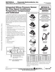
LM3445 Triac Dimmable Offline LED Driver
LM3445 Triac Dimmable Offline LED Driver
LM3445 Triac Dimmable Offline LED Driver

You also want an ePaper? Increase the reach of your titles
YUMPU automatically turns print PDFs into web optimized ePapers that Google loves.
Absolute Maximum Ratings (Notes 1, 2)<br />
If Military/Aerospace specified devices are required,<br />
please contact the National Semiconductor Sales Office/<br />
Distributors for availability and specifications.<br />
BLDR to GND -0.3V to +17V<br />
V CC , GATE, FLTR1 to GND -0.3V to +14V<br />
ISNS to GND<br />
-0.3V to +2.5V<br />
ASNS, DIM, FLTR2, COFF to<br />
GND<br />
-0.3V to +7.0V<br />
COFF Input Current<br />
100mA<br />
Continuous Power Dissipation Internally Limited<br />
(Note 3)<br />
ESD Susceptibility<br />
HBM (Note 4)<br />
2 kV<br />
Junction Temperature (T J-MAX ) 150°C<br />
Storage Temperature Range<br />
-65°C to +150°C<br />
Maximum Lead Temp.<br />
Range (Soldering) 300°C<br />
Operating Conditions<br />
V CC<br />
Junction Temperature<br />
8.0V to 12V<br />
−40°C to +125°C<br />
<strong>LM3445</strong><br />
Electrical Characteristics Limits in standard type face are for T J = 25°C and those with boldface type apply<br />
over the full Operating Temperature Range ( T J = −40°C to +125°C). Minimum and Maximum limits are guaranteed through test,<br />
design, or statistical correlation. Typical values represent the most likely parametric norm at T J = +25ºC, and are provided for<br />
reference purposes only.<br />
BLEEDER<br />
Symbol Parameter Conditions Min Typ Max Units<br />
V CC SUPPLY<br />
COFF<br />
R BLDR Bleeder resistance to GND I BLDR = 10mA 230 325 Ω<br />
I VCC Operating supply current 2.00 2.85 mA<br />
V CC-UVLO Rising threshold 7.4 7.7 V<br />
Falling threshold 6.0 6.4<br />
Hysterisis 1<br />
V COFF Time out threshold 1.225 1.276 1.327 V<br />
R COFF Off timer sinking impedance 33 60 Ω<br />
t COFF Restart timer 180 µs<br />
CURRENT LIMIT<br />
V ISNS ISNS limit threshold 1.174 1.269 1.364 V<br />
t ISNS Leading edge blanking time 125 ns<br />
INTERNAL PWM RAMP<br />
Current limit reset delay 180 µs<br />
ISNS limit to GATE delay ISNS = 0 to 1.75V step 33 ns<br />
f RAMP Frequency 5.85 kHz<br />
V RAMP Valley voltage 0.96 1.00 1.04 V<br />
Peak voltage 2.85 3.00 3.08<br />
D RAMP Maximum duty cycle 96.5 98.0 %<br />
DIM DECODER<br />
t ANG_DET Angle detect rising threshold Observed on BLDR pin 6.79 7.21 7.81 V<br />
V ASNS ASNS filter delay 4 µs<br />
ASNS VMAX 3.85 4.00 4.15 V<br />
I ASNS ASNS drive capability sink V ASNS = 2V 7.6 mA<br />
ASNS drive capability source V ASNS = 2V -4.3<br />
DIM low sink current V DIM = 1V 1.65 2.80<br />
DIM High source current V DIM = 4V -4.00 -3.00<br />
V DIM DIM low voltage PWM input voltage<br />
threshold<br />
0.9 1.33 V<br />
DIM high voltage 2.33 3.15<br />
V TSTH Tri-state threshold voltage Apply to FLTR1 pin 4.87 5.25 V<br />
R DIM DIM comparator tri-state impedance 10 MΩ<br />
3 www.national.com