LM3445 Triac Dimmable Offline LED Driver
LM3445 Triac Dimmable Offline LED Driver
LM3445 Triac Dimmable Offline LED Driver

You also want an ePaper? Increase the reach of your titles
YUMPU automatically turns print PDFs into web optimized ePapers that Google loves.
<strong>LM3445</strong><br />
<strong>Triac</strong> <strong>Dimmable</strong> <strong>Offline</strong> <strong>LED</strong> <strong>Driver</strong><br />
General Description<br />
The <strong>LM3445</strong> is an adaptive constant off-time AC/DC buck<br />
(step-down) constant current controller designed to be compatible<br />
with triac dimmers. The <strong>LM3445</strong> provides a constant<br />
current for illuminating high power <strong>LED</strong>s and includes a triac<br />
dim decoder. The dim decoder allows wide range <strong>LED</strong> dimming<br />
using standard triac dimmers. The high frequency capable<br />
architecture allows the use of small external passive<br />
components. The <strong>LM3445</strong> includes a bleeder circuit to ensure<br />
proper triac operation by allowing current flow while the line<br />
voltage is low to enable proper firing of the triac. A passive<br />
PFC circuit ensures good power factor by drawing current directly<br />
from the line for most of the cycle, and provides a<br />
constant positive voltage to the buck regulator. Additional<br />
features include thermal shutdown, current limit and V CC under-voltage<br />
lockout.<br />
Features<br />
February 10, 2009<br />
■ <strong>Triac</strong> dim decoder circuit for <strong>LED</strong> dimming<br />
■ Application voltage range 80V AC – 270V AC<br />
■ Capable of controlling <strong>LED</strong> currents greater than 1A<br />
■ Adjustable switching frequency<br />
■ Low quiescent current<br />
■ Adaptive programmable off-time allows for constant ripple<br />
current<br />
■ Thermal shutdown<br />
■ No 120Hz flicker<br />
■ Low profile 10 pin MSOP Package<br />
■ Patent pending drive architecture<br />
Applications<br />
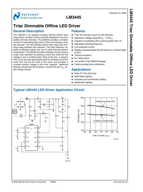
Typical <strong>LM3445</strong> <strong>LED</strong> <strong>Driver</strong> Application Circuit<br />
■ Retro Fit <strong>Triac</strong> Dimming<br />
■ Solid State Lighting<br />
■ Industrial and Commercial Lighting<br />
■ Residential Lighting<br />
<strong>LM3445</strong> <strong>Triac</strong> <strong>Dimmable</strong> <strong>Offline</strong> <strong>LED</strong> <strong>Driver</strong><br />
30060305<br />
30060301<br />
© 2009 National Semiconductor Corporation 300603 www.national.com
<strong>LM3445</strong><br />
Connection Diagram<br />
Top View<br />
10-Pin MSOP<br />
NS Package Number MUB10A<br />
30060303<br />
Ordering Information<br />
Order Number Spec. Package<br />
Type<br />
NSC Package<br />
Drawing<br />
Top Mark<br />
Supplied As<br />
<strong>LM3445</strong>MM NOPB MSOP-10 MUB10A SULB 1000 Units, Tape and Reel<br />
<strong>LM3445</strong>MMX NOPB MSOP-10 MUB10A SULB 3500 Units, Tape and Reel<br />
Pin Descriptions<br />
Pin # Name Description<br />
1 ASNS PWM output of the triac dim decoder circuit. Outputs a 0 to 4V PWM signal with a duty cycle proportional to<br />
the triac dimmer on-time.<br />
2 FLTR1 First filter input. The 120Hz PWM signal from ASNS is filtered to a DC signal and compared to a 1 to 3V, 5.85<br />
kHz ramp to generate a higher frequency PWM signal with a duty cycle proportional to the triac dimmer firing<br />
angle. Pull above 4.9V (typical) to tri-state DIM.<br />
3 DIM Input/output dual function dim pin. This pin can be driven with an external PWM signal to dim the <strong>LED</strong>s. It may<br />
also be used as an output signal and connected to the DIM pin of other <strong>LM3445</strong> or <strong>LED</strong> drivers to dim multiple<br />
<strong>LED</strong> circuits simultaneously.<br />
4 COFF OFF time setting pin. A user set current and capacitor connected from the output to this pin sets the constant<br />
OFF time of the switching controller.<br />
5 FLTR2 Second filter input. A capacitor tied to this pin filters the PWM dimming signal to supply a DC voltage to control<br />
the <strong>LED</strong> current. Could also be used as an analog dimming input.<br />
6 GND Circuit ground connection.<br />
7 ISNS <strong>LED</strong> current sense pin. Connect a resistor from main switching MOSFET source, ISNS to GND to set the<br />
maximum <strong>LED</strong> current.<br />
8 GATE Power MOSFET driver pin. This output provides the gate drive for the power switching MOSFET of the buck<br />
controller.<br />
9 V CC Input voltage pin. This pin provides the power for the internal control circuitry and gate driver.<br />
10 BLDR Bleeder pin. Provides the input signal to the angle detect circuitry as well as a current path through a switched<br />
230Ω resistor to ensure proper firing of the triac dimmer.<br />
www.national.com 2
Absolute Maximum Ratings (Notes 1, 2)<br />
If Military/Aerospace specified devices are required,<br />
please contact the National Semiconductor Sales Office/<br />
Distributors for availability and specifications.<br />
BLDR to GND -0.3V to +17V<br />
V CC , GATE, FLTR1 to GND -0.3V to +14V<br />
ISNS to GND<br />
-0.3V to +2.5V<br />
ASNS, DIM, FLTR2, COFF to<br />
GND<br />
-0.3V to +7.0V<br />
COFF Input Current<br />
100mA<br />
Continuous Power Dissipation Internally Limited<br />
(Note 3)<br />
ESD Susceptibility<br />
HBM (Note 4)<br />
2 kV<br />
Junction Temperature (T J-MAX ) 150°C<br />
Storage Temperature Range<br />
-65°C to +150°C<br />
Maximum Lead Temp.<br />
Range (Soldering) 300°C<br />
Operating Conditions<br />
V CC<br />
Junction Temperature<br />
8.0V to 12V<br />
−40°C to +125°C<br />
<strong>LM3445</strong><br />
Electrical Characteristics Limits in standard type face are for T J = 25°C and those with boldface type apply<br />
over the full Operating Temperature Range ( T J = −40°C to +125°C). Minimum and Maximum limits are guaranteed through test,<br />
design, or statistical correlation. Typical values represent the most likely parametric norm at T J = +25ºC, and are provided for<br />
reference purposes only.<br />
BLEEDER<br />
Symbol Parameter Conditions Min Typ Max Units<br />
V CC SUPPLY<br />
COFF<br />
R BLDR Bleeder resistance to GND I BLDR = 10mA 230 325 Ω<br />
I VCC Operating supply current 2.00 2.85 mA<br />
V CC-UVLO Rising threshold 7.4 7.7 V<br />
Falling threshold 6.0 6.4<br />
Hysterisis 1<br />
V COFF Time out threshold 1.225 1.276 1.327 V<br />
R COFF Off timer sinking impedance 33 60 Ω<br />
t COFF Restart timer 180 µs<br />
CURRENT LIMIT<br />
V ISNS ISNS limit threshold 1.174 1.269 1.364 V<br />
t ISNS Leading edge blanking time 125 ns<br />
INTERNAL PWM RAMP<br />
Current limit reset delay 180 µs<br />
ISNS limit to GATE delay ISNS = 0 to 1.75V step 33 ns<br />
f RAMP Frequency 5.85 kHz<br />
V RAMP Valley voltage 0.96 1.00 1.04 V<br />
Peak voltage 2.85 3.00 3.08<br />
D RAMP Maximum duty cycle 96.5 98.0 %<br />
DIM DECODER<br />
t ANG_DET Angle detect rising threshold Observed on BLDR pin 6.79 7.21 7.81 V<br />
V ASNS ASNS filter delay 4 µs<br />
ASNS VMAX 3.85 4.00 4.15 V<br />
I ASNS ASNS drive capability sink V ASNS = 2V 7.6 mA<br />
ASNS drive capability source V ASNS = 2V -4.3<br />
DIM low sink current V DIM = 1V 1.65 2.80<br />
DIM High source current V DIM = 4V -4.00 -3.00<br />
V DIM DIM low voltage PWM input voltage<br />
threshold<br />
0.9 1.33 V<br />
DIM high voltage 2.33 3.15<br />
V TSTH Tri-state threshold voltage Apply to FLTR1 pin 4.87 5.25 V<br />
R DIM DIM comparator tri-state impedance 10 MΩ<br />
3 www.national.com
<strong>LM3445</strong><br />
Symbol Parameter Conditions Min Typ Max Units<br />
CURRENT SENSE COMPARATOR<br />
V FLTR2 FLTR2 open circuit voltage 720 750 780 mV<br />
R FLTR2 FLTR2 impedance 420 kΩ<br />
V OS Current sense comparator offset voltage -4.0 0.1 4.0 mV<br />
GATE DRIVE OUTPUT<br />
V DRVH GATE high saturation I GATE = 50 mA 0.24 0.50 V<br />
V DRVL GATE low saturation I GATE = 100 mA 0.22 0.50<br />
I DRV Peak souce current GATE = V CC /2 -0.77 A<br />
Peak sink current GATE = V CC /2 0.88<br />
t DV Rise time C load = 1 nF 15 ns<br />
Fall time C load = 1 nF 15<br />
THERMAL SHUTDOWN<br />
T SD Thermal shutdown temperature (Note 5) 165 °C<br />
Thermal shutdown hysteresis 20<br />
THERMAL SHUTDOWN<br />
R θJA<br />
MSOP-10 junction to ambient 121 °C/W<br />
Note 1: Absolute maximum ratings are limits beyond which damage to the device may occur. Operating Ratings are conditions for which the device is intended<br />
to be functional, but device parameter specifications may not be guaranteed. For guaranteed specifications and test conditions, see the Electrical Characteristics.<br />
Note 2: All voltages are with respect to the potential at the GND pin, unless otherwise specified.<br />
Note 3: Internal thermal shutdown circuitry protects the device from permanent damage. Thermal shutdown engages at T J = 165°C (typ.) and disengages at T J<br />
= 145°C (typ).<br />
Note 4: Human Body Model, applicable std. JESD22-A114-C.<br />
Note 5: Junction-to-ambient thermal resistance is highly application and board-layout dependent. In applications where high maximum power dissipation exists,<br />
special care must be paid to thermal dissipation issues in board design. In applications where high power dissipation and/or poor package thermal resistance is<br />
present, the maximum ambient temperature may have to be derated. Maximum ambient temperature (T A-MAX ) is dependent on the maximum operating junction<br />
temperature (T J-MAX-OP = 125°C), the maximum power dissipation of the device in the application (P D-MAX ), and the junction-to ambient thermal resistance of the<br />
part/package in the application (R θJA ), as given by the following equation: T A-MAX = T J-MAX-OP – (R θJA × P D-MAX ).<br />
www.national.com 4
Typical Performance Characteristics<br />
f SW vs Input Line Voltage<br />
Efficiency vs Input Line Voltage<br />
<strong>LM3445</strong><br />
30060304<br />
30060305<br />
BLDR Resistor vs Temperature<br />
V CC UVLO vs Temperature<br />
Min On-Time (t ON ) vs Temperature<br />
30060306<br />
Off Threshold (C11) vs Temperature<br />
30060307<br />
30060308<br />
30060309<br />
5 www.national.com
<strong>LM3445</strong><br />
Normalized Variation in f SW over V BUCK Voltage<br />
Leading Edge Blanking Variation Over Temperature<br />
30060310<br />
30060372<br />
www.national.com 6
Simplified Internal Block Diagram<br />
<strong>LM3445</strong><br />
30060311<br />
FIGURE 1. Simplified Block Diagram<br />
7 www.national.com
<strong>LM3445</strong><br />
Application Information<br />
FUNCTIONAL DESCRIPTION<br />
The <strong>LM3445</strong> contains all the necessary circuitry to build a linepowered<br />
(mains powered) constant current <strong>LED</strong> driver whose<br />
output current can be controlled with a conventional triac dimmer.<br />
OVERVIEW OF PHASE CONTROL DIMMING<br />
A basic "phase controlled" triac dimmer circuit is shown in<br />
Figure 2.<br />
30060312<br />
FIGURE 2. Basic <strong>Triac</strong> Dimmer<br />
An RC network consisting of R1, R2, and C1 delay the turn<br />
on of the triac until the voltage on C1 reaches the trigger voltage<br />
of the diac. Increasing the resistance of the potentiometer<br />
(wiper moving downward) increases the turn-on delay which<br />
decreases the on-time or "conduction angle" of the triac (θ).<br />
This reduces the average power delivered to the load. Voltage<br />
waveforms for a simple triac dimmer are shown in Figure 3.<br />
Figure 3a shows the full sinusoid of the input voltage. Even<br />
when set to full brightness, few dimmers will provide 100%<br />
on-time, i.e., the full sinusoid.<br />
FIGURE 3. Line Voltage and Dimming Waveforms<br />
30060313<br />
Figure 3b shows a theoretical waveform from a dimmer. The<br />
on-time is often referred to as the "conduction angle" and may<br />
be stated in degrees or radians. The off-time represents the<br />
delay caused by the RC circuit feeding the triac. The off-time<br />
be referred to as the "firing angle" and is simply 180° - θ.<br />
Figure 3c shows a waveform from a so-called reverse phase<br />
dimmer, sometimes referred to as an electronic dimmer.<br />
These typically are more expensive, microcontroller based<br />
dimmers that use switching elements other than triacs. Note<br />
that the conduction starts from the zero-crossing, and terminates<br />
some time later. This method of control reduces the<br />
noise spike at the transition.<br />
Since the <strong>LM3445</strong> has been designed to assess the relative<br />
on-time and control the <strong>LED</strong> current accordingly, most phasecontrol<br />
dimmers, both forward and reverse phase, may be<br />
used with success.<br />
www.national.com 8
Theory of Operation<br />
Refer to figure 4 below which shows the <strong>LM3445</strong> along with<br />
basic external circuitry.<br />
<strong>LM3445</strong><br />
30060301<br />
FIGURE 4. <strong>LM3445</strong> Schematic<br />
9 www.national.com
<strong>LM3445</strong><br />
SENSING THE RECTIFIED TRIAC WAVEFORM<br />
A bridge rectifier, BR1, converts the line (mains) voltage (5c)<br />
into a series of half-sines as shown in 5b. Figure 5a shows a<br />
typical voltage waveform after diode D3 (valley fill circuit, or<br />
V BUCK ).<br />
30060315<br />
FIGURE 5. Voltage Waveforms After Bridge Rectifier<br />
Without <strong>Triac</strong> Dimming<br />
Figure 6c and 6b show typical triac dimmed voltage waveforms<br />
before and after the bridge rectifier. Figure 6a shows a<br />
typical triac dimmed voltage waveform after diode D3 (valley<br />
fill circuit, or V BUCK ).<br />
30060316<br />
FIGURE 6. Voltage Waveforms After Bridge Rectifier With<br />
<strong>Triac</strong> Dimming<br />
<strong>LM3445</strong> LINE SENSING CIRCUITRY<br />
An external series pass regulator (R2, D1, and Q1) translates<br />
the rectified line voltage to a level where it can be sensed by<br />
the BLDR pin on the <strong>LM3445</strong>.<br />
30060317<br />
FIGURE 7. <strong>LM3445</strong> AC Line Sense Circuitry<br />
D1 is typically a 15V zener diode which forces transistor Q1<br />
to “stand-off” most of the rectified line voltage. Having no capacitance<br />
on the source of Q1 allows the voltage on the BLDR<br />
pin to rise and fall with the rectified line voltage as the line<br />
voltage drops below zener voltage D1 (see the section on<br />
Angle Detect).<br />
A diode-capacitor network (D2, C5) is used to maintain the<br />
voltage on the VCC pin while the voltage on the BLDR pin<br />
goes low. This provides the supply voltage to operate the<br />
<strong>LM3445</strong>.<br />
Resistor R5 is used to bleed charge out of any stray capacitance<br />
on the BLDR node and may be used to provide the<br />
necessary holding current for the dimmer when operating at<br />
light output currents.<br />
TRIAC HOLDING CURRENT RESISTOR<br />
In order to emulate an incandescent light bulb (essentially a<br />
resistor) with any <strong>LED</strong> driver, the existing triac will require a<br />
small amount of holding current throughout the AC line cycle.<br />
An external resistor (R5) needs to be placed on the source of<br />
Q1 to GND to perform this function. Most existing triac dimmers<br />
only require a few milliamps of current to hold them on.<br />
A few “less expensive” triacs sold on the market will require<br />
a bit more current. The value of resistor R5 will depend on:<br />
• What type of triac the <strong>LM3445</strong> will be used with<br />
• How many light fixtures are running off of the triac<br />
With a single <strong>LM3445</strong> circuit on a common triac dimmer, a<br />
holding current resistor between 3 kΩ and 5 kΩ will be required.<br />
As the number of <strong>LM3445</strong> circuits is added to a single<br />
dimmer, the holding resistor R5’s resistance can be increased.<br />
A few triac dimmers will require a resistor as low as<br />
1 kΩ or lower for a single <strong>LM3445</strong> circuit. The trade-off will be<br />
www.national.com 10
performance vs efficiency. As the holding resistor R5 is increased,<br />
the overall efficiency per <strong>LM3445</strong> will also increase.<br />
ANGLE DETECT<br />
The Angle Detect circuit uses a comparator with a fixed<br />
threshold voltage of 7.21V to monitor the BLDR pin to determine<br />
whether the triac is on or off. The output of the comparator<br />
drives the ASNS buffer and also controls the Bleeder<br />
circuit. A 4 µs delay line on the output is used to filter out noise<br />
that could be present on this signal.<br />
The output of the Angle Detect circuit is limited to a 0V to 4.0V<br />
swing by the buffer and presented to the ASNS pin. R1 and<br />
C3 comprise a low-pass filter with a bandwidth on the order<br />
of 1.0Hz.<br />
The Angle Detect circuit and its filter produce a DC level which<br />
corresponds to the duty cycle (relative on-time) of the triac<br />
dimmer. As a result, the <strong>LM3445</strong> will work equally well with<br />
50Hz or 60Hz line voltages.<br />
BLEEDER<br />
While the BLDR pin is below the 7.21V threshold, the bleeder<br />
MOSFET is on to place a small load (230Ω) on the series pass<br />
regulator. This additional load is necessary to complete the<br />
circuit through the triac dimmer so that the dimmer delay circuit<br />
can operate correctly. Above 7.21V, the bleeder resistor<br />
is removed to increase efficiency.<br />
FLTR1 PIN<br />
The FLTR1 pin has two functions. Normally, it is fed by ASNS<br />
through filter components R1 and C3 and drives the dim decoder.<br />
However, if the FLTR1 pin is tied above 4.9V (typical),<br />
e.g., to VCC, the Ramp Comparator is tri-stated, disabling the<br />
dim decoder. See the Master/Slave section.<br />
DIM DECODER<br />
The ramp generator produces a 5.85 kHz saw tooth wave with<br />
a minimum of 1.0V and a maximum of 3.0V. The filtered ASNS<br />
signal enters pin FLTR1 where it is compared against the<br />
output of the Ramp Generator.<br />
The output of the ramp comparator will have an on-time which<br />
is inversely proportional to the average voltage level at pin<br />
FLTR1. However, since the FLTR1 signal can vary between<br />
0V and 4.0V (the limits of the ASNS pin), and the Ramp Generator<br />
signal only varies between 1.0V and 3.0V, the output<br />
of the ramp comparator will be on continuously for V FLTR1 <<br />
1.0V and off continuously for V FLTR1 > 3.0V. This allows a decoding<br />
range from 45° to 135° to provide a 0 – 100% dimming<br />
range.<br />
The output of the ramp comparator drives both a commonsource<br />
N-channel MOSFET through a Schmitt trigger and the<br />
DIM pin (see the Master/Slave section for further functions of<br />
the DIM pin). The MOSFET drain is pulled up to 750 mV by a<br />
50 kΩ resistor.<br />
Since the MOSFET inverts the output of the ramp comparator,<br />
the drain voltage of the MOSFET is proportional to the duty<br />
cycle of the line voltage that comes through the triac dimmer.<br />
The amplitude of the ramp generator causes this proportionality<br />
to "hard limit" for duty cycles above 75% and below 25%.<br />
The MOSFET drain signal next passes through an RC filter<br />
comprised of an internal 370 kΩ resistor, and an external capacitor<br />
on pin FLTR2. This forms a second low pass filter to<br />
further reduce the ripple in this signal, which is used as a reference<br />
by the PWM comparator. This RC filter is generally set<br />
to 10Hz.<br />
The net effect is that the output of the dim decoder is a DC<br />
voltage whose amplitude varies from near 0V to 750 mV as<br />
the duty cycle of the dimmer varies from 25% to 75%. This<br />
corresponds to conduction angles of 45° to 135°, respectively.<br />
The output voltage of the Dim Decoder directly controls the<br />
peak current that will be delivered by Q2 during its on-time.<br />
See the Buck Converter section for details.<br />
As the triac fires beyond 135°, the DIM decoder no longer<br />
controls the dimming. At this point the <strong>LED</strong>s will dim gradually<br />
for one of two reasons:<br />
1. The voltage at V BUCK decreases and the buck converter<br />
runs out of headroom and causes <strong>LED</strong> current to<br />
decrease as V BUCK decreases.<br />
2. Minimum on-time is reached which fixes the duty-cycle<br />
and therefore reduces the voltage at V BUCK .<br />
The transition from dimming with the DIM decoder to headroom<br />
or minimum on-time dimming is seamless. <strong>LED</strong> currents<br />
from full load to as low as 0.5 mA can be easily achieved.<br />
VALLEY-FILL CIRCUIT<br />
V BUCK supplies the power which drives the <strong>LED</strong> string. Diode<br />
D3 allows V BUCK to remain high while V+ cycles on and off.<br />
V BUCK has a relatively small hold capacitor C10 which reduces<br />
the voltage ripple when the valley fill capacitors are being<br />
charged. However, the network of diodes and capacitors<br />
shown between D3 and C10 make up a "valley-fill" circuit. The<br />
valley-fill circuit can be configured with two or three stages.<br />
The most common configuration is two stages. Figure 8 illustrates<br />
a two and three stage valley-fill circuit.<br />
<strong>LM3445</strong><br />
30060318<br />
FIGURE 8. Two and Three Stage Valley Fill Circuit<br />
11 www.national.com
<strong>LM3445</strong><br />
The valley-fill circuit allows the buck regulator to draw power<br />
throughout a larger portion of the AC line. This allows the capacitance<br />
needed at V BUCK to be lower than if there were no<br />
valley-fill circuit, and adds passive power factor correction<br />
(PFC) to the application. Besides better power factor correction,<br />
a valley-fill circuit allows the buck converter to operate<br />
while separate circuitry translates the dimming information.<br />
This allows for dimming that isn’t subject to 120Hz flicker that<br />
can be perceived by the human eye.<br />
VALLEY-FILL OPERATION<br />
When the “input line is high”, power is derived directly through<br />
D3. The term “input line is high” can be explained as follows.<br />
The valley-fill circuit charges capacitors C7 and C9 in series<br />
(see figure 9) when the input line is high.<br />
30060319<br />
FIGURE 9. Two stage Valley-Fill Circuit when AC Line is<br />
High<br />
A three stage valley-fill circuit performs exactly the same as<br />
two-stage valley-fill circuit except now three capacitors are<br />
now charged in series, and when the line voltage decreases<br />
to:<br />
Diode D3 is reversed biased and three capacitors are in parallel<br />
to each other.<br />
The valley-fill circuit can be optimized for power factor, voltage<br />
hold up and overall application size and cost. The<br />
<strong>LM3445</strong> will operate with a single stage or a three stage valley-fill<br />
circuit as well. Resistor R8 functions as a current<br />
limiting resistor during start-up, and during the transition from<br />
series to parallel connection. Resistors R6 and R7 are 1 MΩ<br />
bleeder resistors, and may or may not be necessary for each<br />
application.<br />
BUCK CONVERTER<br />
The <strong>LM3445</strong> is a buck controller that uses a proprietary constant<br />
off-time method to maintain constant current through a<br />
string of <strong>LED</strong>s. While transistor Q2 is on, current ramps up<br />
through the inductor and <strong>LED</strong> string. A resistor R3 senses this<br />
current and this voltage is compared to the reference voltage<br />
at FLTR2. When this sensed voltage is equal to the reference<br />
voltage, transistor Q2 is turned off and diode D10 conducts<br />
the current through the inductor and <strong>LED</strong>s. Capacitor C12<br />
eliminates most of the ripple current seen in the inductor. Resistor<br />
R4, capacitor C11, and transistor Q3 provide a linear<br />
current ramp that sets the constant off-time for a given output<br />
voltage.<br />
The peak voltage of a two stage valley-fill capacitor is:<br />
As the AC line decreases from its peak value every cycle,<br />
there will be a point where the voltage magnitude of the AC<br />
line is equal to the voltage that each capacitor is charged. At<br />
this point diode D3 becomes reversed biased, and the capacitors<br />
are placed in parallel to each other (figure 10), and<br />
V BUCK equals the capacitor voltage.<br />
30060321<br />
FIGURE 10. Two stage Valley-Fill Circuit when AC Line is<br />
Low<br />
www.national.com 12
<strong>LM3445</strong><br />
30060323<br />
FIGURE 11. <strong>LM3445</strong> Buck Regulation Circuit<br />
OVERVIEW OF CONSTANT OFF-TIME CONTROL<br />
A buck converter’s conversion ratio is defined as:<br />
against the voltage of dim decoder output, FLTR2, at which<br />
point Q2 is turned off by the controller.<br />
Constant off-time control architecture operates by simply<br />
defining the off-time and allowing the on-time, and therefore<br />
the switching frequency, to vary as either V IN or V O changes.<br />
The output voltage is equal to the <strong>LED</strong> string voltage (V <strong>LED</strong> ),<br />
and should not change significantly for a given application.<br />
The input voltage or V BUCK in this analysis will vary as the<br />
input line varies. The length of the on-time is determined by<br />
the sensed inductor current through a resistor to a voltage<br />
reference at a comparator. During the on-time, denoted by<br />
t ON , MOSFET switch Q2 is on causing the inductor current to<br />
increase. During the on-time, current flows from V BUCK ,<br />
through the <strong>LED</strong>s, through L2, Q2, and finally through R3 to<br />
ground. At some point in time, the inductor current reaches a<br />
maximum (I L2-PK ) determined by the voltage sensed at R3 and<br />
the ISNS pin. This sensed voltage across R3 is compared<br />
FIGURE 12. Inductor Current Waveform in CCM<br />
30060325<br />
During the off-period denoted by t OFF , the current through L2<br />
continues to flow through the <strong>LED</strong>s via D10.<br />
13 www.national.com
<strong>LM3445</strong><br />
MASTER/SLAVE OPERATION<br />
Multiple <strong>LM3445</strong>s can be configured so that large strings of<br />
<strong>LED</strong>s can be controlled by a single triac dimmer. By doing so,<br />
smooth consistent dimming for multiple <strong>LED</strong> circuits is<br />
achieved.<br />
When the FLTR1 pin is tied above 4.9V (typical), preferably<br />
to VCC, the ramp comparator is tri-stated, disabling the dim<br />
decoder. This allows one or more <strong>LM3445</strong> devices or PWM<br />
<strong>LED</strong> driver devices (slaves) to be controlled by a single<br />
<strong>LM3445</strong> (master) by connecting their DIM pins together.<br />
MASTER/SLAVE CONFIGURATION<br />
National Semiconductor offers an <strong>LM3445</strong> demonstration<br />
PCB for customer evaluation through our website. The following<br />
description and theory uses reference designators that<br />
follow our evaluation PCB. The <strong>LM3445</strong> Master/Slave<br />
schematics are illustrated below (figures 13 - 15) for clarity.<br />
Each board contains a separate circuit for the Master and<br />
Slave function. Both the Master and Slave boards will need<br />
to be modified from their original stand alone function so that<br />
they can be coupled together. Only the Master <strong>LM3445</strong> requires<br />
use of the Master/Slave circuit for any number of<br />
slaves.<br />
MASTER BOARD MODIFICATIONS<br />
• Remove R10 and replace with a BAS40 diode<br />
• Connect TP18 to TP14 (V CC )<br />
• Connect TP17 (gate of Q5) to TP15 (gate of Q2)<br />
SLAVE BOARD(S) MODIFICATIONS<br />
• Remove R11 (disconnects BLDR)<br />
• Tie TP14 (FLTR1) to V CC<br />
MASTER/SLAVE(S) INTERCONNECTION<br />
• Connect TP19 of Master to TP10 of Slave (Master VCC<br />
Control)<br />
• Connect TP6 (DIM pin) of Master to TP6 (DIM pin) of Slave<br />
(Master DIM Control)<br />
MASTER/SLAVE THEORY OF OPERATION<br />
By placing two series diodes on the Master VCC circuit one<br />
forces the master VCC UVLO to become the dominant threshold.<br />
When Master VCC drops below UVLO, GATE stops<br />
switching and the RC timer (>200 µs) rises above the TL431<br />
threshold (2.5V) which in turn pulls down on the gate of the<br />
Slave pass device (Q1).<br />
The valley-fill circuit could consist of one large circuit to power<br />
all <strong>LM3445</strong> series connected, or each <strong>LM3445</strong> circuit could<br />
have a separate valley-fill circuit located near the buck converter.<br />
www.national.com 14
MASTER/SLAVE CONNECTION DIAGRAM<br />
<strong>LM3445</strong><br />
30060326<br />
FIGURE 13. Master Slave Configuration<br />
MASTER/SLAVE BLOCK DIAGRAMS<br />
30060327<br />
FIGURE 14. Master/Slave configuration with Separate Valley-Fill Circuits<br />
15 www.national.com
<strong>LM3445</strong><br />
30060328<br />
FIGURE 15. Master/Slave configuration with One Valley-Fill Circuit<br />
THERMAL SHUTDOWN<br />
Thermal shutdown limits total power dissipation by turning off<br />
the output switch when the IC junction temperature exceeds<br />
165°C. After thermal shutdown occurs, the output switch<br />
doesn’t turn on until the junction temperature drops to approximately<br />
145°C.<br />
www.national.com 16
Design Guide<br />
DETERMINING DUTY-CYCLE (D)<br />
Duty cycle (D) approximately equals:<br />
With efficiency of the buck converter in mind:<br />
<strong>LM3445</strong><br />
Substitute equations and rearrange:<br />
With efficiency considered:<br />
For simplicity, choose efficiency between 75% and 85%.<br />
CALCULATING OFF-TIME<br />
The “Off-Time” of the <strong>LM3445</strong> is set by the user and remains<br />
fairly constant as long as the voltage of the <strong>LED</strong> stack remains<br />
constant. Calculating the off-time is the first step in determining<br />
the switching frequency of the converter, which is integral<br />
in determining some external component values.<br />
PNP transistor Q3, resistor R4, and the <strong>LED</strong> string voltage<br />
define a charging current into capacitor C11. A constant current<br />
into a capacitor creates a linear charging characteristic.<br />
Resistor R4, capacitor C11 and the current through resistor<br />
R4 (i COLL ), which is approximately equal to V <strong>LED</strong> /R4, are all<br />
fixed. Therefore, dv is fixed and linear, and dt (t OFF ) can now<br />
be calculated.<br />
Off-time, and switching frequency can now be calculated using<br />
the equations above.<br />
SETTING THE SWITCHING FREQUENCY<br />
Selecting the switching frequency for nominal operating conditions<br />
is based on tradeoffs between efficiency (better at low<br />
frequency) and solution size/cost (smaller at high frequency).<br />
The input voltage to the buck converter (V BUCK ) changes with<br />
both line variations and over the course of each half-cycle of<br />
the input line voltage. The voltage across the <strong>LED</strong> string will,<br />
however, remain constant, and therefore the off-time remains<br />
constant.<br />
The on-time, and therefore the switching frequency, will vary<br />
as the V BUCK voltage changes with line voltage. A good design<br />
practice is to choose a desired nominal switching frequency<br />
knowing that the switching frequency will decrease as the line<br />
voltage drops and increase as the line voltage increases (see<br />
figure 16).<br />
Common equations for determining duty cycle and switching<br />
frequency in any buck converter:<br />
30060310<br />
Therefore:<br />
FIGURE 16. Graphical Illustration of Switching<br />
Frequency vs V BUCK<br />
17 www.national.com
<strong>LM3445</strong><br />
The off-time of the <strong>LM3445</strong> can be programmed for switching<br />
frequencies ranging from 30 kHz to over 1 MHz. A trade-off<br />
between efficiency and solution size must be considered<br />
when designing the <strong>LM3445</strong> application.<br />
The maximum switching frequency attainable is limited only<br />
by the minimum on-time requirement (200 ns).<br />
Worst case scenario for minimum on time is when V BUCK is at<br />
its maximum voltage (AC high line) and the <strong>LED</strong> string voltage<br />
(V <strong>LED</strong> ) is at its minimum value.<br />
The maximum voltage seen by the Buck Converter is:<br />
Given a fixed inductor value, L, this equation states that the<br />
change in the inductor current over time is proportional to the<br />
voltage applied across the inductor.<br />
During the on-time, the voltage applied across the inductor is,<br />
V L(ON-TIME) = V BUCK - (V <strong>LED</strong> + V DS(Q2) + I L2 x R3)<br />
Since the voltage across the MOSFET switch (Q2) is relatively<br />
small, as is the voltage across sense resistor R3, we<br />
can simplify this to approximately,<br />
V L(ON-TIME) = V BUCK - V <strong>LED</strong><br />
During the off-time, the voltage seen by the inductor is approximately:<br />
V L(OFF-TIME) = V <strong>LED</strong><br />
The value of V L(OFF-TIME) will be relatively constant, because<br />
the <strong>LED</strong> stack voltage will remain constant. If we rewrite the<br />
equation for an inductor inserting what we know about the<br />
circuit during the off-time, we get:<br />
INDUCTOR SELECTION<br />
The controlled off-time architecture of the <strong>LM3445</strong> regulates<br />
the average current through the inductor (L2), and therefore<br />
the <strong>LED</strong> string current. The input voltage to the buck converter<br />
(V BUCK ) changes with line variations and over the course of<br />
each half-cycle of the input line voltage. The voltage across<br />
the <strong>LED</strong> string is relatively constant, and therefore the current<br />
through R4 is constant. This current sets the off-time of the<br />
converter and therefore the output volt-second product<br />
(V <strong>LED</strong> x off-time) remains constant. A constant volt-second<br />
product makes it possible to keep the ripple through the inductor<br />
constant as the voltage at V BUCK varies.<br />
Re-arranging this gives:<br />
From this we can see that the ripple current (Δi) is proportional<br />
to off-time (t OFF ) multiplied by a voltage which is dominated<br />
by V <strong>LED</strong> divided by a constant (L2).<br />
These equations can be rearranged to calculate the desired<br />
value for inductor L2.<br />
Where:<br />
Finally:<br />
30060340<br />
FIGURE 17. <strong>LM3445</strong> External Components of the Buck<br />
Converter<br />
The equation for an ideal inductor is:<br />
Refer to “Design Example” section of the datasheet to better<br />
understand the design process.<br />
www.national.com 18
SETTING THE <strong>LED</strong> CURRENT<br />
The <strong>LM3445</strong> constant off-time control loop regulates the peak<br />
inductor current (I L2 ). The average inductor current equals the<br />
average <strong>LED</strong> current (I AVE ). Therefore the average <strong>LED</strong> current<br />
is regulated by regulating the peak inductor current.<br />
This is important to calculate because this peak current multiplied<br />
by the sense resistor R3 will determine when the<br />
internal comparator is tripped. The internal comparator turns<br />
the control MOSFET off once the peak sensed voltage reaches<br />
750 mV.<br />
<strong>LM3445</strong><br />
FIGURE 18. Inductor Current Waveform in CCM<br />
30060325<br />
Knowing the desired average <strong>LED</strong> current, I AVE and the nominal<br />
inductor current ripple, Δi L , the peak current for an application<br />
running in continuous conduction mode (CCM) is<br />
defined as follows:<br />
Current Limit: Under normal circumstances, the trip voltage<br />
on the PWM comparator would be less than or equal to 750<br />
mV, depending on the amount of dimming. However, if there<br />
is a short circuit or an excessive load on the output, higher<br />
than normal switch currents will cause a voltage above 1.27V<br />
on the ISNS pin which will trip the I-LIM comparator. The I-<br />
LIM comparator will reset the RS latch, turning off Q2. It will<br />
also inhibit the Start Pulse Generator and the COFF comparator<br />
by holding the COFF pin low. A delay circuit will<br />
prevent the start of another cycle for 180 µs.<br />
VALLEY FILL CAPACITORS<br />
Determining voltage rating and capacitance value of the valley-fill<br />
capacitors:<br />
The maximum voltage seen by the valley-fill capacitors is:<br />
Or, the maximum, or "undimmed", <strong>LED</strong> current would then be,<br />
This is, of course, if the capacitors chosen have identical capacitance<br />
values and split the line voltage equally. Often a<br />
20% difference in capacitance could be observed between<br />
like capacitors. Therefore a voltage rating margin of 25% to<br />
50% should be considered.<br />
19 www.national.com
<strong>LM3445</strong><br />
Determining the capacitance value of the valley-fill capacitors:<br />
The valley fill capacitors should be sized to supply energy to<br />
the buck converter (V BUCK ) when the input line is less than its<br />
peak divided by the number of stages used in the valley fill<br />
(t X ). The capacitance value should be calculated when the<br />
triac is not firing, i.e. when full <strong>LED</strong> current is being drawn by<br />
the <strong>LED</strong> string. The maximum power is delivered to the <strong>LED</strong><br />
string at this time, and therefore the most capacitance will be<br />
needed.<br />
operate at much lower and higher input voltages a range<br />
is needed to illustrate the design process.<br />
2. How many stages are implemented in the valley-fill circuit<br />
(1, 2 or 3).<br />
In this example the most common valley-fill circuit will be used<br />
(two stages).<br />
30060354<br />
FIGURE 20. AC Line with Firing Angles<br />
30060352<br />
FIGURE 19. Two Stage Valley-Ffill V BUCK Voltage with no<br />
TRIAC Dimming<br />
Figure 21 show three triac dimmed waveforms. One can easily<br />
see that the peak voltage (V PEAK ) from 0° to 90° will always<br />
be:<br />
From the above illustration and the equation for current in a<br />
capacitor, i = C x dV/dt, the amount of capacitance needed at<br />
V BUCK will be calculated as follows:<br />
At 60Hz, and a valley-fill circuit of two stages, the hold up time<br />
(t X ) required at V BUCK is calculated as follows. The total angle<br />
of an AC half cycle is 180° and the total time of a half AC line<br />
cycle is 8.33 ms. When the angle of the AC waveform is at<br />
30° and 150°, the voltage of the AC line is exactly ½ of its<br />
peak. With a two stage valley-fill circuit, this is the point where<br />
the <strong>LED</strong> string switches from power being derived from AC<br />
line to power being derived from the hold up capacitors (C7<br />
and C9). 60° out of 180° of the cycle or 1/3 of the cycle the<br />
power is derived from the hold up capacitors (1/3 x 8.33 ms<br />
= 2.78 ms). This is equal to the hold up time (dt) from the<br />
above equation, and dv is the amount of voltage the circuit is<br />
allowed to droop. From the next section (“Determining Maximum<br />
Number of Series Connected <strong>LED</strong>s Allowed”) we know<br />
the minimum V BUCK voltage will be about 45V for a 90V AC to<br />
135V AC line. At 90V AC low line operating condition input, ½ of<br />
the peak voltage is 64V. Therefore with some margin the voltage<br />
at V BUCK can not droop more than about 15V (dv). (i) is<br />
equal to (P OUT /V BUCK ), where P OUT is equal to (V <strong>LED</strong> x I <strong>LED</strong> ).<br />
Total capacitance (C7 in parallel with C9) can now be calculated.<br />
See “ Design Example" section for further calculations<br />
of the valley-fill capacitors.<br />
Determining Maximum Number of Series Connected<br />
<strong>LED</strong>s Allowed:<br />
The <strong>LM3445</strong> is an off-line buck topology <strong>LED</strong> driver. A buck<br />
converter topology requires that the input voltage (V BUCK ) of<br />
the output circuit must be greater than the voltage of the <strong>LED</strong><br />
stack (V <strong>LED</strong> ) for proper regulation. One must determine what<br />
the minimum voltage observed by the buck converter will be<br />
before the maximum number of <strong>LED</strong>s allowed can be determined.<br />
Two variables will have to be determined in order to<br />
accomplish this.<br />
1. AC line operating voltage. This is usually 90V AC to<br />
135V AC for North America. Although the <strong>LM3445</strong> can<br />
Once the triac is firing at an angle greater than 90° the peak<br />
voltage will lower and equal to:<br />
The voltage at V BUCK with a valley fill stage of two will look<br />
similar to the waveforms of figure 22.<br />
The purpose of the valley fill circuit is to allow the buck converter<br />
to pull power directly off of the AC line when the line<br />
voltage is greater than its peak voltage divided by two (two<br />
stage valley fill circuit). During this time, the capacitors within<br />
the valley fill circuit (C7 and C8) are charged up to the peak<br />
of the AC line voltage. Once the line drops below its peak<br />
divided by two, the two capacitors are placed in parallel and<br />
deliver power to the buck converter. One can now see that if<br />
the peak of the AC line voltage is lowered due to variations in<br />
the line voltage, or if the triac is firing at an angle above 90°,<br />
the DC offset (V DC ) will lower. V DC is the lowest value that<br />
voltage V BUCK will encounter.<br />
Example:<br />
Line voltage = 90V AC to 135V AC<br />
Valley-Fill = two stage<br />
Depending on what type and value of capacitors are used,<br />
some derating should be used for voltage droop when the<br />
www.national.com 20
capacitors are delivering power to the buck converter. When<br />
the triac is firing at 135° the current through the <strong>LED</strong> string will<br />
be small. Therefore the droop should be small at this point<br />
and a 5% voltage droop should be a sufficient derating. With<br />
this derating, the lowest voltage the buck converter will see is<br />
about 42.5V in this example.<br />
<strong>LM3445</strong><br />
30060355<br />
FIGURE 21. AC Line with Various Firing Angles<br />
30060356<br />
FIGURE 22. V BUCK Waveforms with Various Firing Angles<br />
To determine how many <strong>LED</strong>s can be driven, take the minimum<br />
voltage the buck converter will see (42.5V) and divide it<br />
by the worst case forward voltage drop of a single <strong>LED</strong>.<br />
Example: 42.5V/3.7V = 11.5 <strong>LED</strong>s (11 <strong>LED</strong>s with margin)<br />
OUTPUT CAPACITOR<br />
A capacitor placed in parallel with the <strong>LED</strong> or array of <strong>LED</strong>s<br />
can be used to reduce the <strong>LED</strong> current ripple while keeping<br />
the same average current through both the inductor and the<br />
<strong>LED</strong> array. With a buck topology the output inductance (L2)<br />
can now be lowered, making the magnetics smaller and less<br />
expensive. With a well designed converter, you can assume<br />
that all of the ripple will be seen by the capacitor, and not the<br />
<strong>LED</strong>s. One must ensure that the capacitor you choose can<br />
handle the RMS current of the inductor. Refer to<br />
manufacture’s datasheets to ensure compliance. Usually an<br />
X5R or X7R capacitor between 1 µF and 10 µF of the proper<br />
voltage rating will be sufficient.<br />
SWITCHING MOSFET<br />
The main switching MOSFET should be chosen with efficiency<br />
and robustness in mind. The maximum voltage across the<br />
switching MOSFET will equal:<br />
The average current rating should be greater than:<br />
I DS-MAX = I <strong>LED</strong>(-AVE) (D MAX )<br />
RE-CIRCULATING DIODE<br />
The <strong>LM3445</strong> Buck converter requires a re-circulating diode<br />
D10 (see the Typical Application circuit figure 4) to carry the<br />
inductor current during the MOSFET Q2 off-time. The most<br />
efficient choice for D10 is a diode with a low forward drop and<br />
near-zero reverse recovery time that can withstand a reverse<br />
voltage of the maximum voltage seen at V BUCK . For a common<br />
110V AC ± 20% line, the reverse voltage could be as high as<br />
190V.<br />
The current rating must be at least:<br />
Or:<br />
I D = 1 - (D MIN ) x I <strong>LED</strong>(AVE)<br />
21 www.national.com
<strong>LM3445</strong><br />
Design Example<br />
The following design example illustrates the process of calculating<br />
external component values.<br />
Known:<br />
1. Input voltage range (90V AC – 135V AC )<br />
2. Number of <strong>LED</strong>s in series = 7<br />
3. Forward voltage drop of a single <strong>LED</strong> = 3.6V<br />
4. <strong>LED</strong> stack voltage = (7 x 3.6V) = 25.2V<br />
Choose:<br />
1. Nominal switching frequency, f SW-TARGET = 250 kHz<br />
2. I <strong>LED</strong>(AVE) = 400 mA<br />
3. Δi (usually 15% - 30% of I<strong>LED</strong>(AVE) ) = (0.30 x 400 mA) =<br />
120 mA<br />
4. Valley fill stages (1,2, or 3) = 2<br />
5. Assumed minimum efficiency = 80%<br />
Calculate:<br />
1. Calculate minimum voltage V BUCK equals:<br />
5. Calculate C11 and R4:<br />
6. Choose current through R4: (between 50 µA and 100 µA)<br />
70 µA<br />
7. Use a standard value of 365 kΩ<br />
8. Calculate C11:<br />
9.<br />
10. Use standard value of 120 pF<br />
11. Calculate ripple current: 400 mA X 0.30 = 120 mA<br />
12. Calculate inductor value at t OFF = 3 µs:<br />
2. Calculate maximum voltage V BUCK equals:<br />
3. Calculate t OFF at V BUCK nominal line voltage:<br />
13. Choose C10: 1.0 µF 200V<br />
14. Calculate valley-fill capacitor values: V AC low line =<br />
90V AC , V BUCK minimum equals 60V (no triac dimming at<br />
maximum <strong>LED</strong> current). Set droop for 20V maximum at<br />
full load and low line.<br />
4. Calculate t ON(MIN) at high line to ensure that<br />
t ON(MIN) > 200 ns:<br />
i) equals P OUT /V BUCK (270 mA), dV equals 20V, dt equals<br />
2.77 ms, and then C TOTAL equals 37 µF. Therefore C7 =<br />
C9 = 22 µF<br />
www.national.com 22
<strong>LM3445</strong> Design Example 1:<br />
Input = 90V AC<br />
to 135V AC<br />
, V <strong>LED</strong><br />
= 7 x HB <strong>LED</strong> String Application @ 400 mA<br />
<strong>LM3445</strong><br />
30060369<br />
23 www.national.com
<strong>LM3445</strong><br />
Bill of Materials<br />
Qty Ref Des Description Mfr Mfr PN<br />
1 U1 IC, CTRLR, DRVR-<strong>LED</strong>, MSOP10 NSC <strong>LM3445</strong>MM<br />
1 BR1 Bridge Rectifiier, SMT, 400V, 800 mA DiodesInc HD04-T<br />
1 L1 Common mode filter DIP4NS, 900 mA, 700<br />
µH<br />
Panasonic<br />
ELF-11090E<br />
1 L2 Inductor, SHLD, SMT, 1A, 470 µH Coilcraft MSS1260-474-KLB<br />
2 L3, L4 Diff mode inductor, 500 mA 1 mH Coilcraft MSS1260-105KL-KLB<br />
1 L5 Bead Inductor, 160Ω, 6A Steward HI1206T161R-10<br />
3 C1, C2, C15 Cap, Film, X2Y2, 12.5MM, 250V AC , 20%, 10<br />
nF<br />
Panasonic<br />
ECQ-U2A103ML<br />
1 C3 Cap, X7R, 0603, 16V, 10%, 470 nF MuRata GRM188R71C474KA88D<br />
1 C4 Cap, X7R, 0603, 16V, 10%, 100 nF MuRata GRM188R71C104KA01D<br />
2 C5, C6 Cap, X5R, 1210, 25V, 10%, 22 µF MuRata GRM32ER61E226KE15L<br />
2 C7, C9 Cap, AL, 200V, 105C, 20%, 33 µF UCC EKXG201ELL330MK20S<br />
1 C10 Cap, Film, 250V, 5%, 10 nF Epcos B32521C3103J<br />
1 C12 Cap, X7R, 1206, 50V, 10%, 1.0 uF Kemet C1206F105K5RACTU<br />
1 C11 Cap, C0G, 0603, 100V, 5%, 120 pF MuRata GRM1885C2A121JA01D<br />
1 C13 Cap, X7R, 0603, 50V, 10%, 1.0 nF Kemet C0603C102K5RACTU<br />
1 C14 Cap, X7R, 0603, 50V, 10%, 22 nF Kemet C0603C223K5RACTU<br />
1 D1 Diode, ZNR, SOT23, 15V, 5% OnSemi BZX84C15LT1G<br />
2 D2, D13 Diode, SCH, SOD123, 40V, 120 mA NXP BAS40H<br />
4 D3, D4, D8, D9 Diode, FR, SOD123, 200V, 1A Rohm RF071M2S<br />
1 D10 Diode, FR, SMB, 400V, 1A OnSemi MURS140T3G<br />
1 D11 IC, SHNT, ADJ, SOT23, 2.5V, 0.5% TI TL431BIDBZR<br />
1 D12 TVS, VBR = 144V Fairchild SMBJ130CA<br />
1 R1 Resistor, 0603, 1%, 280 kΩ Panasonic ERJ-3EKF2803V<br />
1 R2 Resistor, 1206, 1%, 100 kΩ Panasonic ERJ-8ENF1003V<br />
1 R3 Resistor, 1210, 5%, 1.8Ω Panasonic ERJ-14RQJ1R8U<br />
1 R4 Resistor, 0603, 1%, 576 kΩ Panasonic ERJ-3EKF5763V<br />
1 R5 Resistor, 1206, 1%, 1.00 kΩ Panasonic ERJ-8ENF1001V<br />
2 R6, R7 Resistor, 0805, 1%, 1.00 MΩ Rohm MCR10EZHF1004<br />
2 R8, R10 Resistor, 1206, 0.0Ω Yageo RC1206JR-070RL<br />
1 R9 Resistor, 1812, 0.0Ω<br />
1 R11 Resistor, 0603, 0.0Ω Yageo RC0603JR-070RL<br />
1 R12 Resistor, 0603, 1%, 33.2 kΩ Panasonic ERJ-3EKF3322V<br />
1 R13 Resistor, 0603, 1%, 2.0 kΩ Panasonic ERJ-3EKF2001V<br />
1 R14 Resistor, 0805, 1%, 3.3 MΩ Rohm MCR10EZHF3304<br />
1 RT1 Thermistor, 120V, 1.1A, 50Ω @ 25°C Thermometrics CL-140<br />
2 Q1, Q2 XSTR, NFET, DPAK, 300V, 4A Fairchild FQD7N30TF<br />
1 Q3 XSTR, PNP, SOT23, 300V, 500 mA Fairchild MMBTA92<br />
1 Q5 XSTR, NFET, SOT23, 100V, 170 mA Fairchild BSS123<br />
1 J1 Terminal Block 2 pos Phoenix Contact 1715721<br />
1 F1 Fuse, 125V, 1,25A bel SSQ 1.25<br />
www.national.com 24
Physical Dimensions inches (millimeters) unless otherwise noted<br />
<strong>LM3445</strong><br />
MSOP-10 Pin Package (MM)<br />
For Ordering, Refer to Ordering Information Table<br />
NS Package Number MUB10A<br />
25 www.national.com
<strong>LM3445</strong> <strong>Triac</strong> <strong>Dimmable</strong> <strong>Offline</strong> <strong>LED</strong> <strong>Driver</strong><br />
Notes<br />
For more National Semiconductor product information and proven design tools, visit the following Web sites at:<br />
Products<br />
Design Support<br />
Amplifiers www.national.com/amplifiers WEBENCH® Tools www.national.com/webench<br />
Audio www.national.com/audio App Notes www.national.com/appnotes<br />
Clock and Timing www.national.com/timing Reference Designs www.national.com/refdesigns<br />
Data Converters www.national.com/adc Samples www.national.com/samples<br />
Interface www.national.com/interface Eval Boards www.national.com/evalboards<br />
LVDS www.national.com/lvds Packaging www.national.com/packaging<br />
Power Management www.national.com/power Green Compliance www.national.com/quality/green<br />
Switching Regulators www.national.com/switchers Distributors www.national.com/contacts<br />
LDOs www.national.com/ldo Quality and Reliability www.national.com/quality<br />
<strong>LED</strong> Lighting www.national.com/led Feedback/Support www.national.com/feedback<br />
Voltage Reference www.national.com/vref Design Made Easy www.national.com/easy<br />
PowerWise® Solutions www.national.com/powerwise Solutions www.national.com/solutions<br />
Serial Digital Interface (SDI) www.national.com/sdi Mil/Aero www.national.com/milaero<br />
Temperature Sensors www.national.com/tempsensors SolarMagic www.national.com/solarmagic<br />
Wireless (PLL/VCO) www.national.com/wireless Analog University® www.national.com/AU<br />
THE CONTENTS OF THIS DOCUMENT ARE PROVIDED IN CONNECTION WITH NATIONAL SEMICONDUCTOR CORPORATION<br />
(“NATIONAL”) PRODUCTS. NATIONAL MAKES NO REPRESENTATIONS OR WARRANTIES WITH RESPECT TO THE ACCURACY<br />
OR COMPLETENESS OF THE CONTENTS OF THIS PUBLICATION AND RESERVES THE RIGHT TO MAKE CHANGES TO<br />
SPECIFICATIONS AND PRODUCT DESCRIPTIONS AT ANY TIME WITHOUT NOTICE. NO LICENSE, WHETHER EXPRESS,<br />
IMPLIED, ARISING BY ESTOPPEL OR OTHERWISE, TO ANY INTELLECTUAL PROPERTY RIGHTS IS GRANTED BY THIS<br />
DOCUMENT.<br />
TESTING AND OTHER QUALITY CONTROLS ARE USED TO THE EXTENT NATIONAL DEEMS NECESSARY TO SUPPORT<br />
NATIONAL’S PRODUCT WARRANTY. EXCEPT WHERE MANDATED BY GOVERNMENT REQUIREMENTS, TESTING OF ALL<br />
PARAMETERS OF EACH PRODUCT IS NOT NECESSARILY PERFORMED. NATIONAL ASSUMES NO LIABILITY FOR<br />
APPLICATIONS ASSISTANCE OR BUYER PRODUCT DESIGN. BUYERS ARE RESPONSIBLE FOR THEIR PRODUCTS AND<br />
APPLICATIONS USING NATIONAL COMPONENTS. PRIOR TO USING OR DISTRIBUTING ANY PRODUCTS THAT INCLUDE<br />
NATIONAL COMPONENTS, BUYERS SHOULD PROVIDE ADEQUATE DESIGN, TESTING AND OPERATING SAFEGUARDS.<br />
EXCEPT AS PROVIDED IN NATIONAL’S TERMS AND CONDITIONS OF SALE FOR SUCH PRODUCTS, NATIONAL ASSUMES NO<br />
LIABILITY WHATSOEVER, AND NATIONAL DISCLAIMS ANY EXPRESS OR IMPLIED WARRANTY RELATING TO THE SALE<br />
AND/OR USE OF NATIONAL PRODUCTS INCLUDING LIABILITY OR WARRANTIES RELATING TO FITNESS FOR A PARTICULAR<br />
PURPOSE, MERCHANTABILITY, OR INFRINGEMENT OF ANY PATENT, COPYRIGHT OR OTHER INTELLECTUAL PROPERTY<br />
RIGHT.<br />
LIFE SUPPORT POLICY<br />
NATIONAL’S PRODUCTS ARE NOT AUTHORIZED FOR USE AS CRITICAL COMPONENTS IN LIFE SUPPORT DEVICES OR<br />
SYSTEMS WITHOUT THE EXPRESS PRIOR WRITTEN APPROVAL OF THE CHIEF EXECUTIVE OFFICER AND GENERAL<br />
COUNSEL OF NATIONAL SEMICONDUCTOR CORPORATION. As used herein:<br />
Life support devices or systems are devices which (a) are intended for surgical implant into the body, or (b) support or sustain life and<br />
whose failure to perform when properly used in accordance with instructions for use provided in the labeling can be reasonably expected<br />
to result in a significant injury to the user. A critical component is any component in a life support device or system whose failure to perform<br />
can be reasonably expected to cause the failure of the life support device or system or to affect its safety or effectiveness.<br />
National Semiconductor and the National Semiconductor logo are registered trademarks of National Semiconductor Corporation. All other<br />
brand or product names may be trademarks or registered trademarks of their respective holders.<br />
Copyright© 2009 National Semiconductor Corporation<br />
For the most current product information visit us at www.national.com<br />
National Semiconductor<br />
Americas Technical<br />
Support Center<br />
Email: support@nsc.com<br />
Tel: 1-800-272-9959<br />
National Semiconductor Europe<br />
Technical Support Center<br />
Email: europe.support@nsc.com<br />
German Tel: +49 (0) 180 5010 771<br />
English Tel: +44 (0) 870 850 4288<br />
National Semiconductor Asia<br />
Pacific Technical Support Center<br />
Email: ap.support@nsc.com<br />
National Semiconductor Japan<br />
Technical Support Center<br />
Email: jpn.feedback@nsc.com<br />
www.national.com