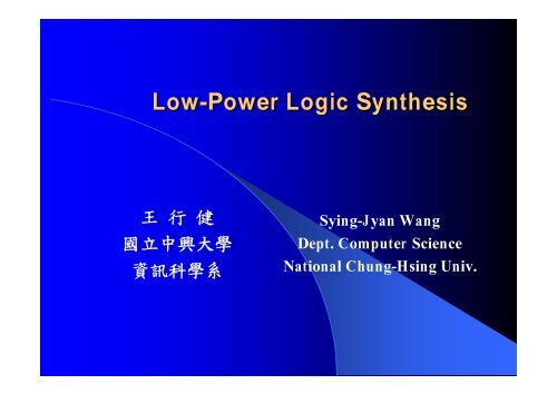
Low-Power Logic Synthesis
Low-Power Logic Synthesis
Low-Power Logic Synthesis

You also want an ePaper? Increase the reach of your titles
YUMPU automatically turns print PDFs into web optimized ePapers that Google loves.
<strong>Low</strong>-<strong>Power</strong> <strong>Logic</strong> <strong>Synthesis</strong><br />
王 行 健<br />
國 立 中 興 大 學<br />
資 訊 科 學 系<br />
Sying-Jyan Wang<br />
Dept. Computer Science<br />
National Chung-Hsing Univ.
Outline<br />
• Overview<br />
– <strong>Power</strong> model<br />
– <strong>Low</strong>-power design techniques<br />
• <strong>Low</strong> <strong>Power</strong> <strong>Logic</strong> <strong>Synthesis</strong><br />
• Switching Activity Reduction<br />
– Sequential<br />
– Combinational<br />
• Retiming-Based Approach<br />
• Preliminary Results<br />
• Conclusion and Future Work<br />
NCHUCS 2
<strong>Power</strong> Model<br />
• Total power<br />
P total<br />
= P s<br />
+ P d<br />
+ P sc<br />
– P s<br />
: Static power due to leakage current<br />
– P d<br />
: Short circuit current due to switching transient<br />
– P d<br />
: Charge and discharge of capacitance<br />
• Dynamic power (P d<br />
) is usually the dominant<br />
factor in CMOS technology<br />
NCHUCS 3
Dynamic <strong>Power</strong><br />
• Dynamic power of a CMOS gate<br />
1<br />
2<br />
Pavg = × CL<br />
× VDD<br />
× fp<br />
× N<br />
2<br />
– C L : Load capacitance<br />
– V DD : <strong>Power</strong> supply voltage<br />
– f p : Clock frequency<br />
– N: Average # of gate output transition (switching<br />
activity) per cycle<br />
NCHUCS 4
<strong>Low</strong>-<strong>Power</strong> Design Techniques<br />
• Can be applied in any<br />
level of the design process<br />
• Various technologies can<br />
be applied simultaneously<br />
• Goal of optimization<br />
– Reduce C L<br />
– Reduce V DD<br />
– Reduce N<br />
– Clock frequency is NOT a<br />
target<br />
Architectural<br />
RTL<br />
<strong>Logic</strong><br />
Circuit<br />
Physical<br />
NCHUCS 5
Architecture Level Techniques<br />
• Sleep Mode<br />
– Deactivate non-operating functional units<br />
– Require little hardware and design complexity<br />
• Asynchronous data processing<br />
– Conduct computation only when necessary<br />
– Reduce switching activities<br />
• Multiple power supply voltages<br />
– Reduce power supply voltages without sacrificing performance<br />
• Architecture transformation<br />
NCHUCS 6
Multiple Supply Voltages<br />
• Basic idea<br />
– Slow down non-critical paths won’t increase cycle time<br />
– So supply voltages of non-critical components can be reduced<br />
• Implementation<br />
– Architecture level: reduce power supply voltage for selected<br />
modules<br />
– <strong>Logic</strong> level: use dual power supply voltages<br />
• Integer Linear Programming (ILP) technique is used to find the best<br />
solution<br />
• Problem: unmatched voltage swing may actually increase power<br />
NCHUCS 7
RTL Techniques<br />
• State encoding for FSM<br />
– Assign adjacent codes to<br />
neighboring states<br />
– To reduce switching<br />
activities in the<br />
combinational logic<br />
• Retiming<br />
– Moving registers to reduce<br />
glitches<br />
00 11<br />
S 1 S 2<br />
S 3<br />
01<br />
NCHUCS 8
Circuit Level Techniques<br />
• Transistor sizing<br />
– Trade silicon area for speed and/or power<br />
• Special flip-flop and latch<br />
– Reduce power in storage elements<br />
• Special logic family<br />
– PPRPL<br />
– PCFL3<br />
– DyCML<br />
– SCSL<br />
– Etc.<br />
NCHUCS 9
<strong>Low</strong>-<strong>Power</strong> <strong>Logic</strong> <strong>Synthesis</strong><br />
• Gate reorganization<br />
– Try to reduce capacitive load<br />
• Pass transistor logic<br />
• Reducing switching activities<br />
– Precomputation<br />
– Partition<br />
– Retiming<br />
NCHUCS 10
Gate Reorganization<br />
• Transform one logic circuit to another that<br />
– Functionally equivalent<br />
– Consume less power<br />
• Apply at<br />
– <strong>Logic</strong> synthesis<br />
– Technology mapping<br />
NCHUCS 11
Pass Transistor <strong>Logic</strong><br />
• Most logic synthesis systems are based on logic<br />
gates<br />
– Processed through Boolean equations<br />
– Implemented with NAND/NOR gates<br />
• Pass transistor logic can implement certain<br />
complex Boolean function efficiently<br />
• In some cases, the power consumption may be<br />
reduced<br />
NCHUCS 12
Switching Activity Reduction<br />
• Basic idea<br />
– Circuit output may be solely decided by part of the<br />
circuit function<br />
– Thus the remaining part of the circuit can be “turned off”<br />
dynamically<br />
• Implementation<br />
– Extract part of the circuit so it can be computed first<br />
• This part of the circuit is usually small<br />
– “Freeze” registers that are not useful if the output is<br />
decided<br />
NCHUCS 13
Example<br />
• Consider the following n-bit comparator<br />
a n–1 …a 0 b n–1 …b 0<br />
Comparator<br />
><br />
– The output is known if a n–1 b n–1 = 10 or 01<br />
– So at least 50% switching activities can be reduced if FFs<br />
corresponding to a n–2 …a 0 and b n–2 …b 0 can be disabled<br />
NCHUCS 14
Precomputation<br />
• Proposed by M. Alidina et al (IEEE Tran. CAD,<br />
1994)<br />
– Synthesize a small “precomputation logic” in addition<br />
to the normal circuit<br />
– This block operated one cycle ahead of the normal<br />
functional circuit (“precomputatiuon”)<br />
– Part of the normal circuit is suspended when the<br />
precomputation condition is true<br />
– The precomputation block is decided by the ODC<br />
(Observability Don’t-Care) of the output function<br />
NCHUCS 15
Basic Architecture<br />
Inputs<br />
Input<br />
Registers<br />
Controllable<br />
Input<br />
Registers<br />
Circuit<br />
Outputs<br />
Precomputaion<br />
<strong>Logic</strong><br />
NCHUCS 16
Precomputation <strong>Logic</strong>— Version 1<br />
x 1<br />
2<br />
‧‧‧‧‧‧<br />
x n<br />
‧‧‧‧‧‧<br />
R1<br />
LE<br />
‧‧‧‧‧‧<br />
A<br />
R2<br />
f<br />
g1<br />
g2<br />
FF<br />
FF<br />
g1=1 ⇒ f = 1<br />
g2=1 ⇒ f = 0<br />
NCHUCS 17
Precomputation <strong>Logic</strong>— Version 1<br />
• Idea<br />
(Cnt’d)<br />
– g1 implements ON-set of f<br />
– g2 implements OFF-set of f<br />
– R1 is disabled if the precomputation condition is TRUE.<br />
• Problem:<br />
– Delay is increased<br />
– Performance is degraded.<br />
NCHUCS 18
Precomputation <strong>Logic</strong>— Version 2<br />
x 1<br />
2<br />
R1<br />
‧‧‧‧<br />
‧‧‧‧<br />
‧‧‧‧<br />
A<br />
R3<br />
f<br />
x n<br />
R2<br />
LE<br />
g1<br />
g2<br />
NCHUCS 19
Self-Timed<br />
Precomputation<br />
x 1<br />
x 2<br />
A<br />
R1<br />
en<br />
x 3<br />
x 4<br />
R2<br />
en<br />
B<br />
f<br />
x 5<br />
g<br />
NCHUCS 20
Partition<br />
• Based on Shannon’s Expansion<br />
f ( x 1<br />
, K,<br />
x ) = x f +<br />
n<br />
i<br />
x<br />
x<br />
i<br />
f<br />
i x i<br />
R<br />
1<br />
f<br />
xi<br />
MUX<br />
f<br />
x 1 … x n<br />
R<br />
2<br />
f<br />
xi<br />
x i<br />
NCHUCS 21
A Retiming-Based Approach<br />
• Move a part of the functional block, rather than<br />
reproduce the block.<br />
– Assume the controlling value of gate G be c<br />
t-1<br />
t-1<br />
x<br />
x 1<br />
1<br />
t-1 R t<br />
t-1<br />
x k 1 C y 1<br />
x k<br />
t<br />
f<br />
t-1<br />
t<br />
t-1<br />
x k+1<br />
G<br />
x k+1<br />
t-1 R 2<br />
x<br />
D<br />
t<br />
t-1<br />
n x n<br />
t-1<br />
C<br />
t-1<br />
y 1<br />
y m<br />
y 2<br />
y 1 ≠c<br />
LE<br />
R 2<br />
D<br />
FF<br />
t<br />
y 2<br />
t<br />
y 1<br />
t<br />
y m<br />
G<br />
f<br />
t<br />
NCHUCS 22
An Example<br />
a<br />
b<br />
c<br />
d<br />
e<br />
f<br />
g<br />
h<br />
i<br />
j<br />
FFa<br />
FFb<br />
FFc<br />
FFd<br />
FFe<br />
FFf<br />
FFg<br />
FFh<br />
FFi<br />
FFj<br />
a'<br />
b'<br />
c'<br />
d'<br />
e'<br />
f'<br />
g'<br />
h'<br />
i'<br />
j'<br />
l<br />
m<br />
n<br />
o<br />
k<br />
p<br />
q<br />
r<br />
z<br />
NCHUCS 23
NCHUCS 24<br />
An Example<br />
An Example (Cnt<br />
(Cnt’d)<br />
d)<br />
a'<br />
b'<br />
c<br />
d<br />
e<br />
f<br />
g<br />
h<br />
i<br />
j<br />
z<br />
k'<br />
r<br />
l<br />
m<br />
n<br />
o<br />
p<br />
q<br />
c'<br />
d'<br />
e'<br />
f'<br />
g'<br />
h'<br />
i'<br />
j'<br />
FFj<br />
E<br />
FFh<br />
E<br />
FFf<br />
E<br />
FFd<br />
E<br />
FFk<br />
FFc<br />
E<br />
FFe<br />
E<br />
FFg<br />
E<br />
FFi<br />
E<br />
k
Data Synchronization<br />
• A retimed block may create synchronization if its<br />
internal node has fanout branches to other gates<br />
• Need extra registers to solve this problem<br />
t-1<br />
x1<br />
t-1<br />
R C<br />
yi t<br />
xk<br />
yj t<br />
t-1<br />
x1<br />
t-1<br />
xk<br />
C<br />
yi t-1<br />
yj t-1<br />
FF<br />
FF<br />
yi t<br />
yj t<br />
NCHUCS 25
Selecting Load-Enabled Registers<br />
• Not all registers can be disabled<br />
– Inputs with fanout to other outputs can not be disabled<br />
– Ex: R 2 can not be disabled<br />
C<br />
FF<br />
yi<br />
R1<br />
D<br />
G<br />
R2<br />
yj<br />
NCHUCS 26
Selecting Retimed Block<br />
• Goal<br />
– Find a logic block which, when retimed, maximizes the<br />
reduced switching activities<br />
– The retimed block must be small in order to reduce the<br />
extra registers<br />
• In our experiment, at most 2 registers are need<br />
• Need to estimate the switching activities<br />
NCHUCS 27
Estimating Switching Activities<br />
• For a net y, let PS(y) be the probability of signal<br />
switching on a clock cycle<br />
PS(<br />
y)<br />
=<br />
=<br />
=<br />
Pr<br />
Pr<br />
Pr<br />
{ a transitionon y at time t}<br />
{<br />
t−1<br />
t<br />
y ⊕ y = 1}<br />
{ t−1<br />
t<br />
( 0) ( 1) ) t−1<br />
t<br />
y = ∧ y = ∨ ( y = 0) ∧ ( y = 1) )}<br />
• ESC(y, c): the expected amount of saved switching<br />
activity if net y is set to value c<br />
ESC(<br />
p)<br />
=<br />
Pr{ y = c}<br />
×∑z<br />
∈<br />
DCNS(<br />
p)<br />
PS(<br />
z)<br />
NCHUCS 28
Algorithm<br />
• Algorithm: Finding the optimal C-cones to be retimed.<br />
• Input: A netlist N and a given k.<br />
• Output: A subset of N to be retimed.<br />
• 1. MaxSaving←0, BestSolution←∅;<br />
• 2. Construct the set of all controlling points CP;<br />
• 3. for (i=1; i MaxSaving) {<br />
• 9. MaxSaving← ES(P);<br />
• 10. BestSolution←P;<br />
}<br />
}<br />
}<br />
11. Report CNS(P);<br />
NCHUCS 29
Experimental Results<br />
NCHUCS 30
CKT NAME New Results Old Paper Reference [1]<br />
cmb 51.76% 22.60% 43.00%<br />
cm138a 52.73% 72.40% 47.00%<br />
majority 55.97% 41.00% 19.00%<br />
cht 43.73% 30.30% 16.00%<br />
cm150 51.27% 22.60% 43.00%<br />
c 43.11% 29.30% 39.00% o<br />
mux 50.20% 52.20% 22.00%<br />
pcle 52.17% 60.40% 30.00%<br />
pcler8 56.09% 41.20% 38.00%<br />
unreg 48.87% 28.40% 18.00%<br />
dalu 43.94% 34.00%<br />
i2 59.40% 65.00%<br />
sao2 41.51% 65.00%<br />
spla 52.31% 41.00%<br />
seq 54.02% 65.00%<br />
apex2 68.40% 42.00%<br />
cps 39.84% 41.00%<br />
duke2 42.57% 23.00%<br />
misex2 48.79% 15.00%<br />
misex3 29.63% 19.00%<br />
e64 66.03% 75.00%<br />
Average 50.11% 40.04% 38.10%<br />
NCHUCS 31
A Comparison<br />
Precomputation Partition Retiming<br />
Area overhead Medium Large Small or No<br />
Critical path delay Unchanged More Unchanged or<br />
Less<br />
Critical path delay<br />
in previous stage<br />
Unchanged or<br />
More<br />
Unchanged<br />
Unchanged or<br />
More<br />
Testability<br />
Problem<br />
Yes No No<br />
NCHUCS 32
Conclusion<br />
• Many low-power design techniques have been developed<br />
– Most of them can be applied simultaneously<br />
– Ad hoc solutions usually work well in practice<br />
• A new logic level low-power synthesis is presented<br />
– The target is to reduce switching activities<br />
– The performance is better than previous methods in terms of<br />
• Reduction in switching activities<br />
• Area<br />
• Critical path delay<br />
NCHUCS 33
Future Works<br />
• Accurate power estimation<br />
• Extension of methods to datapath components<br />
– Should be useful for pipelined ALU<br />
• Retiming circuit to optimize<br />
– <strong>Power</strong><br />
– Speed<br />
• Testability issues<br />
NCHUCS 34