TDA2050 - 32W Hi-Fi Audio Power Amplifier Datasheet - DIY Audio ...
TDA2050 - 32W Hi-Fi Audio Power Amplifier Datasheet - DIY Audio ...
TDA2050 - 32W Hi-Fi Audio Power Amplifier Datasheet - DIY Audio ...

You also want an ePaper? Increase the reach of your titles
YUMPU automatically turns print PDFs into web optimized ePapers that Google loves.
®<br />
<strong>TDA2050</strong><br />
<strong>32W</strong> <strong>Hi</strong>-<strong>Fi</strong> AUDIO POWER AMPLIFIER<br />
HIGH OUTPUT POWER<br />
(50W MUSIC POWER IEC 268.3 RULES)<br />
HIGH OPERATING SUPPLY VOLTAGE (50V)<br />
SINGLE OR SPLIT SUPPLY OPERATIONS<br />
VERY LOW DISTORTION<br />
SHORT CIRCUIT PROTECTION (OUT TO<br />
GND)<br />
THERMAL SHUTDOWN<br />
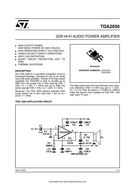
DESCRIPTION<br />
The TDA 2050 is a monolithic integrated circuit in<br />
Pentawatt package, intended for use as an audio<br />
class AB audio amplifier. Thanks to its high power<br />
capability the <strong>TDA2050</strong> is able to provide up to<br />
35W true rms power into 4 ohm load @ THD =<br />
10%, VS = ±18V, f = 1KHz and up to <strong>32W</strong> into<br />
8ohm load @ THD = 10%, VS = ±22V, f = 1KHz.<br />
Moreover, the TDA 2050 delivers typically 50W<br />
music power into 4 ohm load over 1 sec at VS=<br />
22.5V, f = 1KHz.<br />
Pentawatt<br />
ORDERING NUMBERS: <strong>TDA2050</strong>V<br />
<strong>TDA2050</strong>H<br />
The high power and very low harmonic and crossover<br />
distortion (THD = 0.05% typ, @ VS = ±22V,<br />
PO = 0.1 to 15W, RL=8ohm, f = 100Hz to 15KHz)<br />
make the device most suitable for both <strong>Hi</strong><strong>Fi</strong> and<br />
high class TV sets.<br />
TEST AND APPLICATION CIRCUIT<br />
March 2002<br />
This is advanced information on a new product now in development or undergoing evaluation. Details are subject to change without notice.<br />
1/13<br />
Downloaded from http://diy<strong>Audio</strong>Projects.com/
<strong>TDA2050</strong><br />
ABSOLUTE MAXIMUM RATINGS<br />
Symbol Parameter Value Unit<br />
V S Supply Voltage ±25 V<br />
V i Input Voltage V S<br />
V i Differential Input Voltage ±15 V<br />
I O Output Peak Current (internally limited) 5 A<br />
P tot <strong>Power</strong> Dissipation T CASE = 75°C 25 W<br />
T stg , T j Storage and Junction Temperature -40 to 150 °C<br />
PIN CONNECTION (Top view)<br />
SCHEMATIC DIAGRAM<br />
THERMAL DATA<br />
Symbol Description Value Unit<br />
R th j-case Thermal Resistance junction-case Max 3 °C/W<br />
2/13<br />
Downloaded from http://diy<strong>Audio</strong>Projects.com/
<strong>TDA2050</strong><br />
ELECTRICAL CHARACTERISTICS (Refer to the Test Circuit, VS = ±18V, Tamb = 25°C, f = 1 kHz; unless<br />
otherwise specified)<br />
Symbol Parameter Test Condition Min. Typ. Max. Unit<br />
V S Supply Voltage Range ±4.5 ±25 V<br />
I d Quiescent Drain Current V S = ±4.5V<br />
V S = ±25V<br />
I b Input Bias Current V S = ±22V 0.1 0.5 µA<br />
V OS Input Offset Voltage V S = ±22V ±15 mV<br />
I OS Input Offset Current V S = ±22V ±200 nA<br />
P O RMS Output <strong>Power</strong> d = 0.5%<br />
R L = 4Ω<br />
R L = 8Ω<br />
V S = ±22V R L = 8Ω<br />
d = 10%<br />
R L = 4Ω<br />
R L = 8Ω<br />
V S = ±22V R L = 8Ω<br />
Music <strong>Power</strong><br />
IEC268.3 RULES<br />
24<br />
22<br />
30<br />
55<br />
28<br />
18<br />
25<br />
35<br />
22<br />
32<br />
50<br />
90<br />
mA<br />
mA<br />
d = 10%; T = 1s<br />
V S = ±22.5V; R L = 4Ω 50 W<br />
d Total Harmonic Distortion R L = 4Ω<br />
f = 1kHz, P O = 0.1 to 24W<br />
f = 100Hz to 10kHz, P O = 0.1 to 18W<br />
V S = ±22V R L = 8Ω<br />
f = 1kHz, P O = 0.1 to 20W<br />
f = 100Hz to 10kHz, P O = 0.1 to 15W<br />
0.03 0.5<br />
0.5<br />
0.02<br />
%<br />
0.5 %<br />
SR Slew Rate 5 8 V/µs<br />
G V Open Loop Voltage Gain 80 dB<br />
G V Closed Loop Voltage Gain 30 30.5 31 dB<br />
BW <strong>Power</strong> Bandwidth (-3dB) R L = 4Ω V i = 200mV 20 to 80,000 Hz<br />
e N Total Input Noise curve A<br />
B = 22Hz to 22kHz<br />
4<br />
5 10<br />
R i Input Resistance (pin 1) 500 kΩ<br />
SVR Supply Voltage Rejection R s = 22kΩ; f = 100Hz;<br />
V ripple = 0.5Vrms 45 dB<br />
η Efficiency P O = 28W; R L = 4Ω 65 %<br />
P O = 25W; R L = 8Ω;<br />
V S = ±22V 67 %<br />
T sd-j Thermal Shut-down<br />
Junction Temperature<br />
150 °C<br />
W<br />
W<br />
W<br />
W<br />
W<br />
W<br />
%<br />
%<br />
µV<br />
µV<br />
3/13<br />
Downloaded from http://diy<strong>Audio</strong>Projects.com/
<strong>TDA2050</strong><br />
<strong>Fi</strong>gure 1: Split Supply Typical Application Circuit<br />
<strong>Fi</strong>gure 2: P.C. Board and Components Layout of the Circuit of <strong>Fi</strong>g. 1 (1:1)<br />
<strong>TDA2050</strong><br />
C2<br />
R3<br />
R2<br />
R1<br />
C3<br />
R4<br />
C7<br />
C5<br />
RL<br />
+Vs<br />
Vi<br />
C1<br />
C4<br />
C6<br />
-Vs<br />
4/13<br />
Downloaded from http://diy<strong>Audio</strong>Projects.com/
<strong>TDA2050</strong><br />
SPLIT SUPPLY APPLICATION SUGGESTIONS<br />
The recommended values of the external components<br />
are those shown on the application circuit<br />
of fig. 2. Different values can be used. The following<br />
table can help the designer.<br />
Component<br />
Recommended<br />
Value<br />
Purpose<br />
Larger than<br />
Recommended Value<br />
R1 22kΩ Input Impedance Increase of Input<br />
Impedance<br />
Smaller than<br />
Recommended Value<br />
Decrease of Input<br />
Impedance<br />
R2 680Ω Feedback Resistor Decrease of Gain (*) Increase of Gain<br />
R3 22kΩ Increase of Gain Decrease of Gain (*)<br />
R4 2.2Ω Frequency Stability Danger of Oscillations<br />
C1 1µF Input Decoupling DC <strong>Hi</strong>gher Low-frequency<br />
cut-off<br />
C2 22µF Inverting Input<br />
DC Decoupling<br />
C3<br />
C4<br />
C5<br />
C6<br />
Increase of Switch<br />
ON/OFF Noise<br />
<strong>Hi</strong>gher Low-frequency<br />
cut-off<br />
100nF Supply Voltage Bypass Danger of Oscillations<br />
220µF Supply Voltage Bypass Danger of Oscillations<br />
C7 0.47µF Frequency Stability Danger of Oscillations<br />
(*) The gain must be higher than 24dB<br />
PRINTED CIRCUIT BOARD<br />
The layout shown in fig. 2 should be adopted by<br />
the designers. If different layouts are used, the<br />
ground points of input 1 and input 2 must be well<br />
decoupled from the ground return of the output in<br />
which a high current flows.<br />
5/13<br />
Downloaded from http://diy<strong>Audio</strong>Projects.com/
<strong>TDA2050</strong><br />
<strong>Fi</strong>gure 3: Single Supply Typical Application Circuit<br />
<strong>Fi</strong>gure 4: P.C. Board and Components Layout of the Circuit of <strong>Fi</strong>g. 3 (1:1)<br />
6/13<br />
Downloaded from http://diy<strong>Audio</strong>Projects.com/
<strong>TDA2050</strong><br />
SINGLE SUPPLY APPLICATION SUGGESTIONS<br />
The recommended values of the external components<br />
are those shown on the application circuit<br />
of fig. 3. Different values can be used. The following<br />
table can help the designer.<br />
Component<br />
Recommended<br />
Value<br />
Purpose<br />
R1, R2, R3 22kΩ Biasing Resistor<br />
R4<br />
680Ω<br />
Feedback Resistors<br />
Larger than<br />
Recommended Value<br />
Smaller than<br />
Recommended Value<br />
Increase of Gain Decrease of Gain (*)<br />
R5 22kΩ Decrease of Gain (*) Increase of Gain<br />
R6 2.2Ω Frequency Stability Danger of Oscillations<br />
C1 2.2µF Input Decoupling DC <strong>Hi</strong>gher Low-frequency<br />
cut-off<br />
C2 100µF Supply Voltage Rejection Worse Turn-off Transient<br />
Worse Turn-on Delay<br />
C3 1000µF Supply Voltage Bypass Danger of Oscillations<br />
Worse of Turn-off<br />
Transient<br />
C4 22µF Inverting Input DC<br />
Decoupling<br />
Increase of Switching<br />
ON/OFF<br />
<strong>Hi</strong>gher Low-frequency<br />
cut-off<br />
C5 100nF Supply Voltage Bypass Danger of Oscillations<br />
C6 0.47µF Frequency Stability Danger of Oscillations<br />
C7 1000µF Output DC Decoupling <strong>Hi</strong>gher Low-frequency<br />
cut-off<br />
(*) The gain must be higher than 24dB<br />
NOTE<br />
If the supply voltage is lower than 40V and the<br />
load is 8ohm (or more) a lower value of C2 can<br />
be used (i.e. 22µF).<br />
C7 can be larger than 1000uF only if the supply<br />
voltage does not exceed 40V.<br />
TYPICAL CHARACTERISTICS (Split Supply Test Circuit unless otherwise specified)<br />
<strong>Fi</strong>gure 5: Output <strong>Power</strong> vs. Supply Voltage<br />
<strong>Fi</strong>gure 6: Distortion vs. Output <strong>Power</strong><br />
7/13<br />
Downloaded from http://diy<strong>Audio</strong>Projects.com/
<strong>TDA2050</strong><br />
<strong>Fi</strong>gure 7: Output <strong>Power</strong> vs. Supply Voltage<br />
<strong>Fi</strong>gure 8: Distortion vs. Output <strong>Power</strong><br />
<strong>Fi</strong>gure. 9: Distortion vs. Frequency<br />
<strong>Fi</strong>gure 10: Distortion vs. Frequency<br />
<strong>Fi</strong>gure 11: Quiescent Current vs. Supply Voltage<br />
<strong>Fi</strong>gure 12: Supply Voltage Rejection vs. Frequency<br />
8/13<br />
Downloaded from http://diy<strong>Audio</strong>Projects.com/
<strong>TDA2050</strong><br />
<strong>Fi</strong>gure 13: Supply Voltage Rejection vs. Frequency<br />
(Single supply) for Different<br />
values of C2 (circuit of fig. 3)<br />
<strong>Fi</strong>gure 16: Total <strong>Power</strong> Dissipation and Efficiency<br />
vs. Output <strong>Power</strong><br />
<strong>Fi</strong>gure 14: Supply Voltage Rejection vs. Frequency<br />
(Single supply) for Different<br />
values of C2 (circuit of fig. 3)<br />
SHORT CIRCUIT PROTECTION<br />
The TDA 2050 has an original circuit which limits<br />
the current of the output transistors. The maximum<br />
output current is a function of the collector<br />
emitter voltage; hence the output transistors work<br />
within their safe operating area. This function can<br />
therefore be considered as being peak power limiting<br />
rather than simple current limiting.<br />
It reduces the possibility that the device gets<br />
damaged during an accidental short circuit from<br />
AC output to ground.<br />
<strong>Fi</strong>gure 15: Total <strong>Power</strong> Dissipation and Efficiency<br />
vs. Output <strong>Power</strong><br />
THERMAL SHUTDOWN<br />
The presence of a thermal limiting circuit offers<br />
the following advantages:<br />
1)An overload on the output (even if it is permanent),<br />
or an above limit ambient temperature<br />
can be easily tolerated since the Tj cannot be<br />
higher than 150°C.<br />
2)The heatsink can have a smaller factor of<br />
safety compared with that of a conventional<br />
circuit. There is no possibility of device damage<br />
due to high junction temperature. If for<br />
any reason, the junction temperature increases<br />
up to 150°C, the thermal shutdown<br />
simply reduces the power dissipation and the<br />
current consumption.<br />
The maximum allowable power dissipation depends<br />
upon the thermal resistance junction-ambi-<br />
9/13<br />
Downloaded from http://diy<strong>Audio</strong>Projects.com/
<strong>TDA2050</strong><br />
ent. <strong>Fi</strong>g. 17 shows this dissipable power as a<br />
function of ambient temperature for different thermal<br />
resistance.<br />
<strong>Fi</strong>gure 17: Maximum Allowable <strong>Power</strong> Dissipation<br />
vs. Ambient Temperature<br />
MOUNTING INSTRUCTIONS<br />
The power dissipated in the circuit must be removed<br />
by adding an external heatsink.<br />
Thanks to the PENTAWATT package, the<br />
heatsink mounting operation is very simple, a<br />
screw or a compression spring (clip) being sufficient.<br />
Between the heatsink and the package is<br />
better to insert a layer of silicon grease, to optimize<br />
the thermal contact; no electrical isolation is<br />
needed between the two surfaces. <strong>Fi</strong>g. 18 shows<br />
an example of heatsink.<br />
Dimension suggestion<br />
The following table shows the length that the<br />
heatsink in fig. 18 must have for several values<br />
of Ptot and Rth.<br />
P tot (W) 12 8 6<br />
Lenght of heatsink (mm) 60 40 30<br />
R th of heatsink (°C/W) 4.2 6.2 8.3<br />
<strong>Fi</strong>gure 18: Example of heat-sink<br />
APPENDIX A<br />
A.1 - MUSIC POWER CONCEPT<br />
MUSIC POWER is (according to the IEC clauses<br />
n.268-3 of Jan 83) the maximum power which the<br />
amplifier is capable of producing across the rated<br />
load resistance (regardless of non linearity) 1 sec<br />
after the application of a sinusoidal input signal of<br />
frequency 1 KHz.<br />
According to this definition our method of measurement<br />
comprises the following steps:<br />
- Set the voltage supply at the maximum operating<br />
value;<br />
- Apply a input signal in the form of a 1KHz tone<br />
burst of 1 sec duration: the repetition period<br />
of the signal pulses is 60 sec;<br />
- The output voltage is measured 1 sec from the<br />
start of the pulse;<br />
- Increase the input voltage until the output signal<br />
shows a THD=10%;<br />
- The music power is then V 2 out /RL, where<br />
Vout is the output voltage measured in the<br />
condition of point 4 and RL is the rated load<br />
impedance;<br />
The target of this method is to avoid excessive<br />
dissipation in the amplifier.<br />
A.2 - INSTANTANEOUS POWER<br />
Another power measurement (MAXIMUM IN-<br />
STANTANEOUS OUTPUT POWER) was proposed<br />
by IEC in 1988 (IEC publication 268-3 subclause<br />
19.A).<br />
We give here only a brief extract of the concept,<br />
and a circuit useful for the measurement.<br />
The supply voltage is set at the maximum operating<br />
value.<br />
The test signal consists of a sinusoidal signal<br />
whose frequency is 20 Hz, to which are added alternate<br />
positive and negative pulses of 50 µs duration<br />
and 500 Hz repetition rate. The amplitude<br />
of the 20 Hz signal is chosen to drive the amplifier<br />
to its voltage clipping limits, while the amplitude of<br />
the pulses takes the amplifier alternately into its<br />
current-overload limits.<br />
10/13<br />
Downloaded from http://diy<strong>Audio</strong>Projects.com/
<strong>TDA2050</strong><br />
A circuit for generating the test signal is given in<br />
fig. 19.<br />
The load network consists of a 40 µF capacitor, in<br />
series with a 1 ohm resistor. The capacitor limits<br />
the current due to the 20 Hz signal to a low value,<br />
whereas for he short pulses the effective load impedance<br />
is of the order of 1 ohm, and a high output<br />
current is produced.<br />
Using this signal and load network the measurement<br />
may be made without causing excessive<br />
dissipation in the amplifier. The dissipation in the<br />
1 ohm resistor is much lower than a rated output<br />
power of the amplifier, because the duty-cycle of<br />
the high output current is low.<br />
By feeding the amplifier output voltage to the X-<br />
plates of an oscilloscope, and the voltage across<br />
the 1 ohm resistor (representing the output current)<br />
to the Y=plates, it is possible to read on the<br />
display the value of the maximum instantaneous<br />
output power.<br />
The result of this test applied at the TDA 2050 is:<br />
PEAK POWER = 100W typ<br />
<strong>Fi</strong>gure 19: Test circuit for peak power measurement<br />
11/13<br />
Downloaded from http://diy<strong>Audio</strong>Projects.com/
<strong>TDA2050</strong><br />
DIM.<br />
mm<br />
inch<br />
MIN. TYP. MAX. MIN. TYP. MAX.<br />
A 4.8 0.189<br />
C 1.37 0.054<br />
D 2.4 2.8 0.094 0.110<br />
D1 1.2 1.35 0.047 0.053<br />
E 0.35 0.55 0.014 0.022<br />
E1 0.76 1.19 0.030 0.047<br />
F 0.8 1.05 0.031 0.041<br />
F1 1.0 1.4 0.039 0.055<br />
G 3.2 3.4 3.6 0.126 0.134 0.142<br />
G1 6.6 6.8 7.0 0.260 0.268 0.276<br />
H2 10.4 0.409<br />
H3 10.05 10.4 0.396 0.409<br />
L 17.55 17.85 18.15 0.691 0.703 0.715<br />
L1 15.55 15.75 15.95 0.612 0.620 0.628<br />
L2 21.2 21.4 21.6 0.831 0.843 0.850<br />
L3 22.3 22.5 22.7 0.878 0.886 0.894<br />
L4 1.29 0.051<br />
L5 2.6 3.0 0.102 0.118<br />
L6 15.1 15.8 0.594 0.622<br />
L7 6.0 6.6 0.236 0.260<br />
L9 2.1 2.7 0.008 0.106<br />
L10 4.3 4.8 0.17 0.189<br />
M 4.23 4.5 4.75 0.167 0.178 0.187<br />
M1 3.75 4.0 4.25 0.148 0.157 0.167<br />
V4<br />
40˚ (typ.)<br />
V5<br />
90˚ (typ.)<br />
Dia 3.65 3.85 0.144 0.152<br />
OUTLINE AND<br />
MECHANICAL DATA<br />
Weight: 2.00gr<br />
Pentawatt V<br />
L<br />
L1<br />
E<br />
M1<br />
A<br />
C<br />
L5<br />
D1<br />
L2<br />
L3<br />
D<br />
V5<br />
M<br />
H2<br />
V4<br />
E<br />
F<br />
E1<br />
H3<br />
G<br />
G1<br />
Dia.<br />
L9<br />
L10<br />
L4<br />
F1<br />
H2<br />
F<br />
V4<br />
L7<br />
L6<br />
RESIN BETWEEN<br />
LEADS<br />
PENTVME<br />
0015981<br />
12/13<br />
Downloaded from http://diy<strong>Audio</strong>Projects.com/
<strong>TDA2050</strong><br />
Information furnished is believed to be accurate and reliable. However, STMicroelectronics assumes no responsibility for the consequences<br />
of use of such information nor for any infringement of patents or other rights of third parties which may result from its use. No license is<br />
granted by implication or otherwise under any patent or patent rights of STMicroelectronics. Specification mentioned in this publication are<br />
subject to change without notice. This publication supersedes and replaces all information previously supplied. STMicroelectronics products<br />
are not authorized for use as critical components in life support devices or systems without express written approval of STMicroelectronics.<br />
The ST logo is a registered trademark of STMicroelectronics<br />
© 2002 STMicroelectronics – Printed in Italy – All Rights Reserved<br />
PENTAWATT® is a Registered Trademark of SGS-THOMSON Microelectronics<br />
STMicroelectronics GROUP OF COMPANIES<br />
Australia - Brazil - Canada - China - <strong>Fi</strong>nland - France - Germany - Hong Kong - India - Israel - Italy - Japan - Malaysia - Malta - Morocco -<br />
Singapore - Spain - Sweden - Switzerland - United Kingdom - United States.<br />
http://www.st.com<br />
13/13<br />
Downloaded from http://diy<strong>Audio</strong>Projects.com/