Hardware Design Guide Revision 0.3 - elinux
Hardware Design Guide Revision 0.3 - elinux
Hardware Design Guide Revision 0.3 - elinux

Create successful ePaper yourself
Turn your PDF publications into a flip-book with our unique Google optimized e-Paper software.
Doc No: WG7310-00-HDG-R03<br />
� Power Trace<br />
� Power trace for VBAT should be 40mil wide. 1.8V trace<br />
should be 18mil wide.<br />
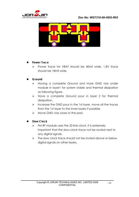
� Ground<br />
� Having a complete Ground and more GND vias under<br />
module in layer1 for system stable and thermal dissipation<br />
as following figure.<br />
� Have a complete Ground pour in layer 2 for thermal<br />
dissipation.<br />
� Increase the GND pour in the 1st layer, move all the traces<br />
from the 1st layer to the inner layers if possible.<br />
� Move GND vias close to the pad.<br />
� Slow Clock<br />
� FM RF module uses the 32-kHz clock, it is extremely<br />
important that the slow-clock trace not be routed next to<br />
any digital signals.<br />
� The slow clock trace should not be routed above or below<br />
digital signals on other layers.<br />
Copyright © JORJIN TECHNOLOGIES INC. LIMITED 2009<br />
CONFIDENTIAL<br />
- 24-