Hardware Design Guide Revision 0.3 - elinux
Hardware Design Guide Revision 0.3 - elinux
Hardware Design Guide Revision 0.3 - elinux

Create successful ePaper yourself
Turn your PDF publications into a flip-book with our unique Google optimized e-Paper software.
Figure 5. SDIO Clock Timing<br />
Table 4. SDIO Timing requirement<br />
Doc No: WG7310-00-HDG-R03<br />
Parameter Min. Max. Unit<br />
fclock Clock frequency, CLK 0 25 MHZ<br />
DC Low/high duty cycle 40 60 %<br />
tWL Pulse duration, CLK low 10 ns<br />
tWH Pulse duration, CLK high 10 ns<br />
tTLH Rise time, CLK 4.3 ns<br />
tTHL Fall time, CLK 3.5 ns<br />
tISU Setup time, input valid before CLK↑ 5 ns<br />
t1H Hold time, input valid after CLK↑ 5 ns<br />
tODLY1 Delay time, CLK↓ to output valid 0 14 ns<br />
TODLY2 Delay time, CLK↓ to output invalid 0 14 ns<br />
4.2. WLAN wSPI Characteristics<br />
The SPI interface signals are shared with the SDIO bus in the WG7310.<br />
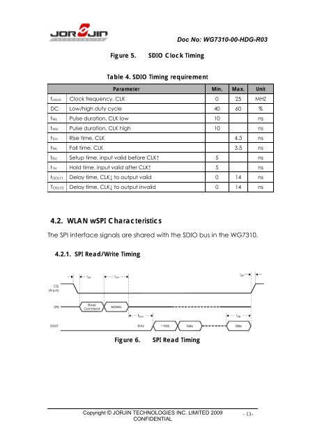
4.2.1. SPI Read/Write Timing<br />
Figure 6. SPI Read Timing<br />
Copyright © JORJIN TECHNOLOGIES INC. LIMITED 2009<br />
CONFIDENTIAL<br />
- 13-