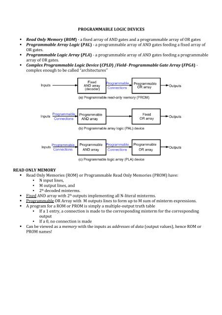
PROGRAMMABLE LOGIC DEVICES Read Only Memory (ROM) - a ...
PROGRAMMABLE LOGIC DEVICES Read Only Memory (ROM) - a ...
PROGRAMMABLE LOGIC DEVICES Read Only Memory (ROM) - a ...

Create successful ePaper yourself
Turn your PDF publications into a flip-book with our unique Google optimized e-Paper software.
<strong>PROGRAMMABLE</strong> <strong>LOGIC</strong> <strong>DEVICES</strong><br />
<strong>Read</strong> <strong>Only</strong> <strong>Memory</strong> (<strong>ROM</strong>) - a fixed array of AND gates and a programmable array of OR gates<br />
Programmable Array Logic (PAL) - a programmable array of AND gates feeding a fixed array of<br />
OR gates.<br />
Programmable Logic Array (PLA) - a programmable array of AND gates feeding a programmable<br />
array of OR gates.<br />
Complex Programmable Logic Device (CPLD) /Field- Programmable Gate Array (FPGA) -<br />
complex enough to be called “architectures”<br />
READ ONLY MEMORY<br />
<strong>Read</strong> <strong>Only</strong> Memories (<strong>ROM</strong>) or Programmable <strong>Read</strong> <strong>Only</strong> Memories (P<strong>ROM</strong>) have:<br />
• N input lines,<br />
• M output lines, and<br />
• 2 N decoded minterms.<br />
Fixed AND array with 2 N outputs implementing all N-literal minterms.<br />
Programmable OR Array with M outputs lines to form up to M sum of minterm expressions.<br />
A program for a <strong>ROM</strong> or P<strong>ROM</strong> is simply a multiple-output truth table<br />
• If a 1 entry, a connection is made to the corresponding minterm for the corresponding<br />
output<br />
• If a 0, no connection is made<br />
Can be viewed as a memory with the inputs as addresses of data (output values), hence <strong>ROM</strong> or<br />
P<strong>ROM</strong> names!
Figure: Block diagram and Internal Logic of a <strong>ROM</strong><br />
Depending on the programming technology and approaches, read-only memories have different<br />
names<br />
1. <strong>ROM</strong> – mask programmed<br />
2. P<strong>ROM</strong> – fuse or antifuse programmed<br />
3. EP<strong>ROM</strong> – erasable floating gate programmed<br />
4. EEP<strong>ROM</strong> or E 2 P<strong>ROM</strong> – electrically erasable floating gate programmed<br />
5. FLASH memory: electrically erasable floating gate with multiple erasure and programming<br />
modes.<br />
Example: A 8 X 4 <strong>ROM</strong> (N = 3 input lines, M= 4 output lines)<br />
• The fixed "AND" array is a “decoder” with 3 inputs and 8 outputs implementing minterms.<br />
• The programmable "OR“ array uses a single line to represent all inputs to an OR gate. An<br />
“X” in the array corresponds to attaching the minterm to the OR<br />
• <strong>Read</strong> Example: For input (A2,A1,A0) = 011, output is (F3,F2,F1,F0 ) = 0011.<br />
• What are functions F3, F2 , F1 and F0 in terms of (A2, A1, A0)
<strong>PROGRAMMABLE</strong> <strong>LOGIC</strong> ARRAY (PLA)<br />
Compared to a <strong>ROM</strong> and a PAL, a PLA is the most flexible having a programmable set of ANDs<br />
combined with a programmable set of ORs.<br />
Advantages<br />
• A PLA can have large N and M permitting implementation of equations that are impractical<br />
for a <strong>ROM</strong> (because of the number of inputs, N, required<br />
• A PLA has all of its product terms connectable to all outputs, overcoming the problem of<br />
the limited inputs to the PAL Ors<br />
• Some PLAs have outputs that can be complemented, adding POS functions<br />
Disadvantages<br />
• Often, the product term count limits the application of a PLA.<br />
• Two-level multiple-output optimization is required to reduce the number of product terms<br />
in an implementation, helping to fit it into a PLA.<br />
• Multi-level circuit capability available in PAL not available in PLA. PLA requires external<br />
connections to do multi-level circuits.<br />
Programmable Logic Array Example<br />
F1=AB’ + AC + A’BC’<br />
F2= (AC+BC)’<br />
What are the equations for F1 and F2<br />
Could the PLA implement the functions without the XOR gates<br />
3-input, 3-output PLA with 4 product terms
Example 6-3 from Mano: Implementing a Combinational Circuit Using a PLA<br />
F1(A,B,C)= Σm(3,5,6,7)<br />
F2(A,B,C)= Σm(1,2,3,7)<br />
The solution is:<br />
<strong>PROGRAMMABLE</strong> ARRAY <strong>LOGIC</strong> (PAL)<br />
The PAL is the opposite of the <strong>ROM</strong>, having a programmable set of ANDs combined with fixed ORs.<br />
Disadvantage<br />
• <strong>ROM</strong> guaranteed to implement any M functions of N inputs. PAL may have too few inputs<br />
to the OR gates.<br />
Advantages<br />
• For given internal complexity, a PAL can have larger N and M<br />
• Some PALs have outputs that can be complemented, adding POS functions<br />
• No multilevel circuit implementations in <strong>ROM</strong> (without external connections from output<br />
to input). PAL has outputs from OR terms as internal inputs to all AND terms, making<br />
implementation of multi-level circuits easier.<br />
Programmable Array Logic Example<br />
4-input, 3-output PAL with fixed, 3-input OR terms<br />
What are the equations for F1 through F4<br />
W(A,B,C,D) = Σm (2,12,13)<br />
X(A,B,C,D) = Σm (7,8,9,10,11,12,13,14,15)<br />
Y(A,B,C,D) = Σm (0,2,3,4,5,6,7,8,10,11,15)<br />
Z(A,B,C,D) = Σm (1,2,8,12,13)<br />
Simplifying the four function to a minimum number of terms results in the following Boolean functions<br />
W= ABC’+A’B’CD’<br />
X = A+BCD<br />
Y = A’B+CD+B’D’<br />
Z = ABC’+A’B’CD’+AC’D’+A’B’C’D = W+AC’D’+A’B’C’D