NANOVEA
NANOVEA
NANOVEA

Create successful ePaper yourself
Turn your PDF publications into a flip-book with our unique Google optimized e-Paper software.
<strong>NANOVEA</strong><br />
Affiliate of Micro Photonics Inc.<br />
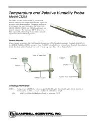
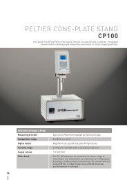
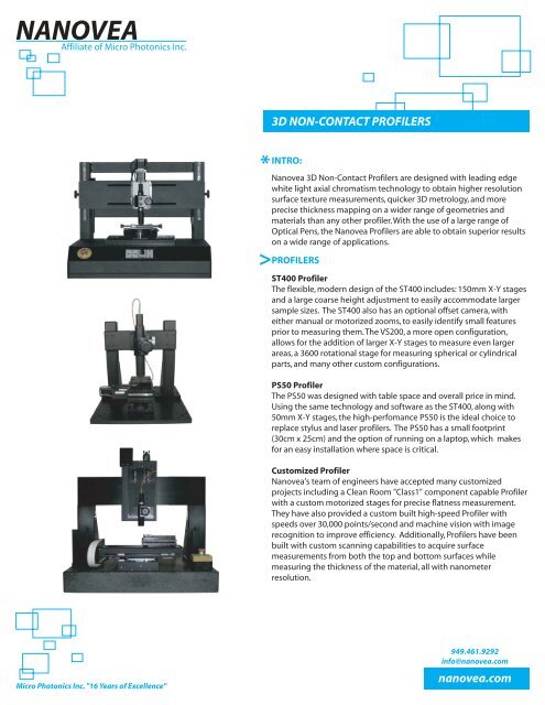
3D NON-CONTACT PROFILERS<br />
INTRO:<br />
Nanovea 3D Non-Contact Profilers are designed with leading edge<br />
white light axial chromatism technology to obtain higher resolution<br />
surface texture measurements, quicker 3D metrology, and more<br />
precise thickness mapping on a wider range of geometries and<br />
materials than any other profiler.With the use of a large range of<br />
Optical Pens, the Nanovea Profilers are able to obtain superior results<br />
on a wide range of applications.<br />
PROFILERS<br />
ST400 Profiler<br />
The flexible, modern design of the ST400 includes: 150mm X-Y stages<br />
and a large coarse height adjustment to easily accommodate larger<br />
sample sizes. The ST400 also has an optional offset camera, with<br />
either manual or motorized zooms, to easily identify small features<br />
prior to measuring them.The VS200, a more open configuration,<br />
allows for the addition of larger X-Y stages to measure even larger<br />
areas, a 3600 rotational stage for measuring spherical or cylindrical<br />
parts, and many other custom configurations.<br />
PS50 Profiler<br />
The PS50 was designed with table space and overall price in mind.<br />
Using the same technology and software as the ST400, along with<br />
50mm X-Y stages, the high-perfomance PS50 is the ideal choice to<br />
replace stylus and laser profilers. The PS50 has a small footprint<br />
(30cm x 25cm) and the option of running on a laptop, which makes<br />
for an easy installation where space is critical.<br />
Customized Profiler<br />
Nanovea's team of engineers have accepted many customized<br />
projects including a Clean Room "Class1" component capable Profiler<br />
with a custom motorized stages for precise flatness measurement.<br />
They have also provided a custom built high-speed Profiler with<br />
speeds over 30,000 points/second and machine vision with image<br />
recognition to improve efficiency. Additionally, Profilers have been<br />
built with custom scanning capabilities to acquire surface<br />
measurements from both the top and bottom surfaces while<br />
measuring the thickness of the material, all with nanometer<br />
resolution.<br />
Micro Photonics Inc. "16 Years of Excellence"<br />
949.461.9292<br />
info@nanovea.com<br />
nanovea.com
Asphalt Surface<br />
Pill Surface<br />
+<br />
AXIAL CHROMATISM PRINCIPLE<br />
Process:<br />
The technique uses a ray of white light that passes through a lens<br />
containing a high-degree of chromatic abberation, creating a<br />
wavelength coded vertical measurement range. The image results<br />
from a specific, focused wavelength which is reflected back from the<br />
surface being measured. If the surface is composed of transparent<br />
or semi-transparent layers, the technique will be able to<br />
simultaneously measure two surfaces, as well as the thickness of the<br />
layer. Some benefits associated with axial chromatism include:<br />
Benefits:<br />
• Zero influence from sample reflectivity variations<br />
• No sample preparation<br />
• Ability to measure high surface angles<br />
• Large Z measurement range<br />
• Measure all materials; transparent/opaque, specular/diffusive,<br />
polished/rough<br />
• Excellent vertical and spatial resolution<br />
OPTIONS HARDWARE PROFILER<br />
• Video Microscope with Turret<br />
• Turret for Optical Pens<br />
• High Speed X-Y Stages (up to 1m/s)<br />
• High Speed Optical Sensor (up to 30KHz)<br />
• AFM Objective<br />
• Near-IR Interferometric Sensor<br />
• 90 º Pens for Inner Bore Measurements.<br />
For More Information See Additional Brochures:<br />
Software and Applications<br />
HARDWARE SPECIFICATIONS<br />
X-Y Axis Travel<br />
Z Axis<br />
X-Y Axis Resolution<br />
Maximum X-Y speed<br />
Rotational Stage<br />
ST400<br />
150 mm *<br />
60 mm<br />
0.1 µm<br />
20 mm/s<br />
Optional **<br />
PS50<br />
50 mm<br />
30 mm<br />
0.1 µm<br />
10 mm/s<br />
n/a<br />
CUSTOM<br />
100 - 600mm<br />
50 - 500mm<br />
0.1- 0.005um<br />
10 - 1000mm/s<br />
Optional **<br />
MEASUREMENT<br />
RANGE<br />
WORKING<br />
DISTANCE (MM)<br />
VERTICAL<br />
RESOLUTION (NM)<br />
VERTICAL<br />
ACCURACY (NM)<br />
SPOT<br />
DIAMETER (µM)<br />
LATERAL<br />
RESOLUTION (µM)<br />
MINIMUM<br />
TRANSPARENT<br />
THICKNESS (µM)<br />
130µm<br />
400µm<br />
1.2mm<br />
3.5mm<br />
12mm<br />
27mm<br />
20µm<br />
300µm<br />
3.3<br />
11<br />
12.7<br />
16.4<br />
29<br />
19.6<br />
0.37<br />
5.68<br />
5<br />
12<br />
25<br />
75<br />
280<br />
600<br />
2<br />
10<br />
MODULAR OPTICAL PENS<br />
20<br />
60<br />
200<br />
400<br />
900<br />
3000<br />
CLASSICAL OPTICAL PENS<br />
10<br />
90<br />
2<br />
2.6<br />
4<br />
8<br />
16<br />
16<br />
3<br />
7.4<br />
1<br />
1.3<br />
2<br />
4<br />
8<br />
8<br />
1.5<br />
3.7<br />
7<br />
15<br />
25<br />
60<br />
200<br />
590<br />
12<br />
25<br />
10mm<br />
24mm<br />
66.9<br />
222.3<br />
300<br />
1500<br />
900<br />
3000<br />
51<br />
1000<br />
25.5<br />
50<br />
425<br />
1570<br />
Micro Photonics Inc. "16 Years of Excellence"<br />
949.461.9292<br />
info@nanovea.com<br />
nanovea.com
<strong>NANOVEA</strong><br />
Affiliate of Micro Photonics Inc.<br />
PROFILER APPLICATIONS<br />
Bond Pad Surface<br />
APPLICATIONS<br />
Semiconductor Technology<br />
• Wafer Flatness<br />
• Critical Dimensions<br />
• Wafer Thickness<br />
Pharmacological<br />
• Tablets, Pills<br />
• Implants<br />
• Coating Thickness<br />
Wafer Surface<br />
•General Materials<br />
• Carbon Fiber<br />
• Ceramic<br />
Electronics<br />
• BGA (Ball Grid Array)<br />
• LED Chip<br />
• Printed Component Height<br />
• Bonding Pad<br />
• Connector<br />
Drill Bit Edge<br />
Optical Components<br />
• Micro Lens<br />
• Optical Gratings<br />
• Diffractive Lens<br />
• Fresnel Lens<br />
Automotive<br />
• Break Disk<br />
• Tire<br />
Other<br />
• Skin Wrinkles and Acne Scars<br />
• Measurement of Teeth<br />
• Sandpaper<br />
• Woven Fabrics<br />
• Micro Channels<br />
• Paper<br />
• Cutting Tools<br />
Micro Photonics Inc. "16 Years of Excellence"<br />
949.461.9292<br />
info@nanovea.com<br />
nanovea.com
<strong>NANOVEA</strong><br />
Affiliate of Micro Photonics Inc.<br />
PROFILER SOFTWARE<br />
SOFTWARE<br />
Nanovea 3D Software<br />
The Nanovea 3D software is the acquisition software that is used with all<br />
Nanovea Profliers. The software permits the user define the size of the area, or<br />
line, to be measured, as well as the lateral resolution of the measurement. The<br />
software also allows three different views of the measurement in real-time:<br />
cross-sectional, top-down and 3-dimensional views. To make it easier to find<br />
and measure small surfaces, a re-centering function allows the user to pointand-click<br />
on the scanned image in order to re-center the next scan to that<br />
specific point; or by use of a point-and click feature from an optional offset<br />
video camera.<br />
Mountains 3D Analysis Software<br />
Optional software package available to all Nanovea Pro.. lers, which provides<br />
a complete set of surface analysis tools. Some of these functions include:<br />
• User-friendly report making and editing<br />
• An extensive list of roughness, flatness, waviness and other surface parameters<br />
• Create 3D images in false color, contour maps and photo simulation<br />
• A variety of filtering, leveling and other surface correction functions<br />
• Ability to create templates to be applied to multiple individual measurements<br />
• Dimensional analysis, surface area, volume, bearing ratio and texture direction<br />
• Grain counting, sorting, and other grain analysis<br />
• Spectral analysis, autocorrelation, and fractal analysis<br />
• Statistical analysis over a population of results<br />
• Ability to export raw data, images, and entire reports<br />
• Create and export .. y-over videos of the surface<br />
• 4D analysis to look at surface changes, as a function of time<br />
• Motif analysis<br />
• Additional functions available, please check with us for more details<br />
Micro Photonics Inc. "16 Years of Excellence"<br />
949.461.9292<br />
info@nanovea.com<br />
nanovea.com