3D Wafer-Level - Yole Developpement
3D Wafer-Level - Yole Developpement
3D Wafer-Level - Yole Developpement

Create successful ePaper yourself
Turn your PDF publications into a flip-book with our unique Google optimized e-Paper software.
<strong>3D</strong><br />
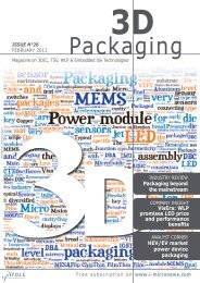
ISSUE N°20<br />
SEPTEMBER 2011<br />
Packaging<br />
Magazine on <strong>3D</strong>IC, TSV, WLP & Embedded die Technologies<br />
FEATURE STORIES<br />
Derivative packaging<br />
roadmaps and<br />
applications<br />
Courtesy of awaiba - Printed on recycled paper<br />
COMPANY INSIGHT<br />
<strong>3D</strong>-IC challenges:<br />
design with test<br />
(Part 1/2)<br />
200μm<br />
WHAT’S INSIDE<br />
<strong>3D</strong> <strong>Wafer</strong>-<strong>Level</strong>-<br />
Packaging of MEMS<br />
gyroscope sensor<br />
with VTI’s CMR3000<br />
Free subscription on www.i-micronews.com
Technology and supply chain challenges<br />
for fabless semiconductor companies<br />
Fabless semiconductor companies constantly face the challenge of designing<br />
competitive products which can easily be manufactured by their manufacturing<br />
partners with good yields. Comprehensive access for their design, test and<br />
quality engineers to the design rules and guidelines is key to implement the<br />
required design for manufacturability (DfM) practices.<br />
This becomes even more critical with the ever widening array of IC packaging<br />
technologies and solutions: how to make the right package platform choice for<br />
a given product What is the most optimized trade-off between electrical and<br />
thermal performance, power consumption, reliability, size, manufacturability<br />
and cost of the packaged integrated circuit How to find the right manufacturing<br />
partners for the chosen technology to minimize risks and costs Should the<br />
technology choices influence the choice of the manufacturing partners, or should<br />
it be the other way round How to access the latest <strong>3D</strong> and wafer level packaging<br />
technologies with controlled risks and without cost penalties How can fabless<br />
companies also influence the evolution and road mapping of the semiconductor<br />
packaging and test industry<br />
These are the hot questions Serma Technologies and <strong>Yole</strong> Développement<br />
propose to debate through a dedicated event jointly organized in Paris<br />
on November 8 to 10, 2011 with invited presentations by worldwide<br />
industrial players of both large global companies and SMEs.<br />
For more information, please contact:<br />
• S. Leroy, <strong>Yole</strong> Développement (leroy@yole.fr)<br />
• B. Crouillère, Serma Technologies (b.crouillere@serma.com)<br />
Successful<br />
Semiconductor<br />
Fabless 2011<br />
November 8 to 10<br />
Crowne Plaza, Paris, France
S E P T E M B E R 2 0 1 1 I S S U E N ° 2 0<br />
E D I T O R I A L<br />
Innovation and technology diversity management<br />
in semiconductor packaging<br />
Back from the Semicon West show in San Francisco, it has now become crystal clear<br />
that <strong>3D</strong> is the number one topic and concern in most semiconductor executives’<br />
minds. I said “semiconductor executives”, not “semiconductor packaging executives”!<br />
Of course, the development of 22nm-CMOS is moving forward and 450mm diameter wafers<br />
are back on the agendas. But no other topic scored even close to <strong>3D</strong> silicon integration in<br />
terms of numbers of dedicated workshops, presentations or exhibition booth totems with the<br />
“<strong>3D</strong>” and “TSV” keywords at Semicon West July 12-14 in San Francisco.<br />
…More surprisingly<br />
<strong>3D</strong> interposers<br />
made of silicon or<br />
glass are confirmed<br />
as a high potential<br />
and expected lasting<br />
trend…<br />
<strong>3D</strong> Integration of memory stacks by means of through silicon vias is a confi rmed big trend.<br />
Same is true for integration of the same stacks on top of a logic IC to enable the so-called<br />
“wide I/O interface” concept for high bandwidth data transfers between the logic part and<br />
the DDR memories. Maybe more surprisingly are <strong>3D</strong> interposers made of silicon or glass<br />
confi rmed as a high potential and expected lasting trend of the industry by several prominent<br />
speakers, whereas one year ago, they were still only considered as a stepping stone to “full<br />
<strong>3D</strong> integration” and accordingly referred to as “2.5D integration”.<br />
The “why’s” of <strong>3D</strong> now all return consensual positive answers and many “how’s” are being<br />
answered with ready-for-production solutions. However some challenges still need to be<br />
addressed, and many agree that more alignment is needed between the industrial players so<br />
as to defi ne standards. Such consortia or standardization committees as Sematech, Semi or<br />
Jedec call for standard wafer thinning, design and test technologies or procedures and they<br />
work toward this goal so as to industrialize solutions with good yields in the future.<br />
Does this mean that all industrial solutions should result from agreed standards to succeed<br />
Nothing would be so untrue, especially concerning the historically and still currently super<br />
wide array of technology options in the semiconductor packaging industry. Whereas some<br />
of the past issues of “<strong>3D</strong> Packaging” focused on the need for standardization, we decided to<br />
focus this August issue to those application areas where diversity and differentiation through<br />
innovation still prevail. Welcome to the diverse packaging and assembly world of MEMS,<br />
LEDs, camera modules and high power chips… a world, which by the way, once invented<br />
“Through Silicon Vias”!<br />
E V E N T S<br />
• Semicon Taiwan<br />
September 7 to 9, 2011 – Taipei, Taiwan<br />
• Itnl <strong>Wafer</strong> <strong>Level</strong> Packaging Conference<br />
October 3 to 6, 2011 – Santa Clara, CA - USA<br />
Jean-Marc Yannou<br />
Project Manager<br />
<strong>Yole</strong> Développement<br />
yannou@yole.fr<br />
• Semicon Europa<br />
October 11 to 13, 2011 – Dresden, Germany<br />
PLATINUM PARTNERS:<br />
3 D P a c k a g i n g 3
S E P T E M B E R 2 0 1 1 I S S U E N ° 2 0<br />
C O N T E N T S<br />
INDUSTRY REVIEW 6<br />
• Off-roadmap’ apps show natural affinity for <strong>3D</strong> packaging<br />
COMPANY INSIGHT 12<br />
• Tong Hsing Electronic Industries: Carving out a ‘niche’ in custom<br />
microelectronics packaging<br />
• Excico ultra-fast laser annealing solutions reach thermal constraint<br />
specifications for BSI and <strong>3D</strong>IC<br />
• Unisem: Cavity packages for volume MEMS applications<br />
• Cadence & GSA Global: <strong>3D</strong>-IC challenges: design with test (Part 1/2)<br />
ANALYST CORNER 24<br />
• Lower costs targeted for HB LED Packaging<br />
• Smartphones morph into sophisticated sensing platforms<br />
WHAT’S INSIDE 28<br />
• <strong>3D</strong> <strong>Wafer</strong>-<strong>Level</strong>-Packaging of MEMS gyroscope sensor<br />
with VTI’s CMR3000<br />
EVENT REVIEW 30<br />
• Advanced Packaging: leading edge technologies bring challenges<br />
and opportunities<br />
FROM I-MICRONEWS.COM<br />
Stay connected with your peers<br />
on i-Micronews.com<br />
Please visit our website to discover the<br />
last top stories in Advanced Packaging:<br />
With 18,000 monthly visitors,<br />
i-Micronews.com provides for Advanced<br />
Packaging area: current news, market<br />
& technological analysis, key leader<br />
interviews, webcasts section, reverse<br />
engineering / costing, events calendar,<br />
latest reports …<br />
> Samsung develops 32GB RDIMM<br />
using <strong>3D</strong> TSV technology<br />
> TSVs ease heat in <strong>3D</strong> ICs<br />
> TI’s NexFET power packaging: a<br />
closer look<br />
GOLD PARTNERS:<br />
4 3 D P a c k a g i n g
Register<br />
today<br />
To attend editorial webcast<br />
Additional webcast topics:<br />
•Oct.18:<br />
Thin wafer handling<br />
& processing<br />
•Oct.26:<br />
PV inverter<br />
Technical innovations<br />
and market trends<br />
•Nov.8:<br />
Glass emergence<br />
into the semiconductor<br />
wafer-processing world<br />
Join the live webcast:<br />
On September 28 th<br />
8:00 AM PDT*<br />
Benefits and<br />
Perspectives<br />
of Cu-Pillar<br />
Bumping<br />
•Nov.29:<br />
High Concentration<br />
Photovoltaics<br />
Technology on the way<br />
to the utility market<br />
Attend live webcast to learn about<br />
the technology and market introduction<br />
to the new flip chip technology which helps<br />
high performance meet lower costs<br />
• Dec. 14:<br />
Future devices<br />
and materials<br />
for power electronics<br />
For more information and to register, please go to<br />
www.i-micronews.com/webcasts.asp or click here<br />
*8:00 AM San Francisco; 5:00 PM Paris, 12:00 AM Tokyo<br />
Hosted by<br />
Powered by<br />
Sponsored by
S E P T E M B E R 2 0 1 1 I S S U E N ° 2 0<br />
INDUSTRY REVIEW<br />
2 axis MEMS accelerometer<br />
to ASIC module assembly<br />
(Courtesy of Freescale)<br />
Some ‘off-roadmap’ apps show<br />
natural affinity for <strong>3D</strong> packaging<br />
Off-roadmap applications like MEMS, image sensors, power components, and LEDs<br />
are outpacing the growth of traditional ICs. As a result, this may usher in a bold new<br />
era of innovation in creating packaging solutions to meet the needs of off-roadmap<br />
apps. This, in turn, will likely prove to be beneficial for more ‘traditional’ ICs too.<br />
Opportunities are clearly emerging in offroadmap<br />
applications, if you take a look<br />
at forecasts in this area. <strong>Yole</strong> estimates<br />
for 2015 put the MEMS market in excess of $17B;<br />
the CMOS image sensor/camera module market at<br />
$13B; the power module market at $4.4B; and the<br />
packaged LED market at $21.6B.<br />
Affinity for <strong>3D</strong> packaging<br />
Some off-roadmap applications appear to have a<br />
natural affinity for <strong>3D</strong> packaging technologies. A close<br />
look at MEMS, in particular, reveals an undeniable<br />
tie to <strong>3D</strong> packaging. As Tomas Bauer, vice<br />
president of sales and business development at Silex<br />
Microsystems, sums it up: <strong>3D</strong> packaging technologies<br />
are “genetically close” to MEMS technologies.<br />
“We’ve seen a lot of the <strong>3D</strong> pioneering work done<br />
by the MEMS manufacturers,” notes Bauer. TSV, for<br />
example, is a key component of the <strong>3D</strong> technologies,<br />
and Silex began supplying commercial parts with<br />
integrated full-wafer-thickness TSVs to a leading<br />
mobile phone manufacturer as early as 2006.<br />
MEMS devices inherently need <strong>3D</strong>IC capabilities to<br />
marry MEMS + IC, explains Peter Himes, Silex’s<br />
vice president of marketing and strategic alliances.<br />
As a result, MEMS companies began implementing<br />
these technologies many years in advance of CMOSonly<br />
foundries.<br />
But the first to actually turn <strong>3D</strong> packaging into a<br />
practice and make volume products was image<br />
sensor packaging, points out Martin Wäny, CEO<br />
6<br />
3 D P a c k a g i n g
I S S U E N ° 2 0 S E P T E M B E R 2 0 1 1<br />
decreases, we can go build BGAs instead. It<br />
just makes more sense in terms of capex and<br />
the flexibility of the production lines.”<br />
need for substrate preparation work—separate<br />
from the IC manufacturing, which enables <strong>3D</strong><br />
packaging.<br />
Fly on NanEye (Courtesy of Awaiba)<br />
and head of CMOS design at Awaiba. Image<br />
sensors have a natural gravitation to <strong>3D</strong><br />
packaging technologies too.<br />
Ultimately, whoever takes the product to<br />
market and interfaces with the end customer<br />
and understands their needs will define the<br />
packaging ideas of <strong>3D</strong> or its alternatives, says<br />
Heinz Ru, vice president of Marketing and<br />
Innovation at Tong Hsing Electronic Industries,<br />
a company that specializes in a wide range of<br />
off-roadmap applications. “<strong>3D</strong> is a new trend,<br />
but in microelectronics packaging, the market<br />
is very competitive and no one can afford<br />
to have ideas or solutions that don’t revolve<br />
around cost. Technologies must be selected<br />
out of necessity—not just because it’s a sexy<br />
new idea—to justify choosing it.”<br />
Focus on cost/flexibility/existing<br />
solutions<br />
Cost and flexibility are two of the most<br />
critical factors for off-roadmap apps. Both are<br />
extremely important but, in this down economy<br />
and increasingly competitive landscape, the<br />
focus is on keeping costs as low as possible.<br />
And it’s important to note that not everyone is<br />
rushing to <strong>3D</strong> packaging, but rather focusing<br />
on making modifications to existing platforms.<br />
Amkor is also focusing on cost and flexibility.<br />
“The recent explosive adoption of MEMS<br />
and sensors in consumer handheld products<br />
has required a transition to lower-cost<br />
MEMS package and test solutions. Amkor<br />
is responding to this market transition by<br />
providing low-stress and cavity package<br />
derivative solutions that borrow from existing<br />
high-volume leadframe and laminate-based<br />
package platforms,” says Russell Shumway,<br />
senior manager of MEMS & Sensor Products at<br />
Amkor.<br />
Impact on business<br />
models/supply chain<br />
A wide variety of business models are being<br />
used for off-roadmap packaging applications—<br />
everything from MEMS foundries to packaging<br />
houses. And the associated supply chains are<br />
also undergoing an evolution of sorts.<br />
Looking at the big picture, Ru cautions that this<br />
is an “emerging, dynamic market,” one that<br />
requires a flexible mindset. He recommends<br />
taking advantage of proven technologies.<br />
“Don’t try to create everything yourself; it isn’t<br />
possible. Look at the resources available in the<br />
market and connect the dots.”<br />
Silex sees a trend emerging in which IC players<br />
are considering pursuing some share of the<br />
evolving market in the ‘mid-end’ segment,<br />
capturing larger share of the total value chain.<br />
“At the same time, we’ve seen a continued<br />
separation of manufacturing and IC packaging.<br />
MEMS players already have <strong>3D</strong> genes and<br />
should be in a good position to capture some<br />
share of this evolving market,” says Bauer.<br />
Another trend, Himes points out, is that the<br />
MEMS foundries are filling a ‘mid-end foundry’<br />
Wäny expects specialty foundries to take over<br />
the lead in the future. “Currently, only a few<br />
packaging houses are active in this area—<br />
mainly in image sensor packaging and for<br />
relatively standardized work,” he says. “A lot of<br />
the substrate work will eventually come from<br />
the specialty foundries that need to supply a<br />
one-stop shop also for power electronics or<br />
MEMS. LED manufacturers will likely set up<br />
large-scale productions for TSV <strong>3D</strong>-like LED<br />
packaging.”<br />
From an OSAT perspective, business model<br />
innovation is critical when integrating devices<br />
from different suppliers in <strong>3D</strong> packages for highvolume<br />
applications. “We’re seeing a strong<br />
fabless MEMS industry emerge because MEMS<br />
foundries and MEMS package assembly and<br />
test can be cost-effectively outsourced in high<br />
volumes—meeting aggressive time-to-market<br />
requirements,” says Lee Smith, vice president<br />
of marketing and business development at<br />
Amkor. He expects the trend to fabless and fab<br />
light business models to continue to escalate,<br />
because application-specific device design and<br />
integration are differentiating factors, and<br />
critical mass is required to develop and invest<br />
in these capital-intensive wafer-level process<br />
technologies.<br />
And not surprisingly, for LEDs, in terms of their<br />
supply chain, much like the rest of the offroadmap<br />
apps, everything remains undecided<br />
and has yet to unfold. “There are several<br />
companies mastering the complete LED supply<br />
chain, including Samsung, Cree, Nichia,<br />
Sharp, OSRAM, and Philips Lumileds. But there<br />
is little standardization in this industry, and a<br />
lot of surprising things can happen down the<br />
road—especially if bold technology choices are<br />
Key components of a packaged LED<br />
(<strong>Yole</strong> Développement, LED Packaging 2011 report)<br />
Right now, most companies aren’t investing<br />
in costly capital equipment for new processes<br />
unless it’s absolutely necessary, says Alan<br />
Evans, Unisem Europe’s head of engineering.<br />
“The idea is that it’s better to do variations on<br />
a theme, so we have MEMS packaging that<br />
can run down QFN and BGA processing lines,”<br />
he explains. “As MEMS volumes increase, it’s<br />
easy to increase the capacity because we have<br />
a lot of that equipment already. If volume<br />
3 D P a c k a g i n g<br />
7
S E P T E M B E R 2 0 1 1 I S S U E N ° 2 0<br />
“Right now nonstandard<br />
apps are<br />
growing faster<br />
than the traditional<br />
IC market,”<br />
explains Lee Smith,<br />
Amkor Technology.<br />
Integrating Silex Microsystems’<br />
TSV technology into MEMS systems<br />
enables reduced form factor and<br />
true wafer-level packaging solutions<br />
(Courtesy of Silex)<br />
made,” notes <strong>Yole</strong>’s Jean-Marc Yannou, technology<br />
and market expert in the field of advanced packaging.<br />
“Innovation is needed to provide differentiation and<br />
drive costs down. Companies who dare to invest,<br />
to reduce costs, need to be bold. Established<br />
companies likely won’t be the ones pushing it, since<br />
they’re happy with the market as it is. We’ll probably<br />
see challengers attempt to take over market share,<br />
especially based on packaging technologies.”<br />
Off-road apps impact on <strong>3D</strong>IC packaging<br />
roadmaps<br />
What roles are companies seeing off-roadmap apps<br />
play in driving the semiconductor IC packaging<br />
roadmap for <strong>3D</strong>ICs/WLP<br />
As Smith points out: Right now non-standard apps<br />
are growing faster than the traditional IC market,<br />
so the result is that more attention is being paid<br />
to look at ways to apply <strong>3D</strong> packaging platform<br />
technologies.<br />
Wäny views off-roadmap markets as still being<br />
important technology drivers, since they have a<br />
real added value in <strong>3D</strong> packaging and most of the<br />
standard (memory) applications see the cost benefit.<br />
In terms of MEMS, there’s an inherent need for<br />
heterogeneous integration, so the market drivers<br />
are different than standard ICs, according to<br />
Himes. “That said, IC needs are driving toward a<br />
different plateau in terms of density, complexity,<br />
and technology (wafer thickness, number of vias,<br />
etc.),” he adds. “So while the applications in MEMS<br />
are different than ICs and the resulting topography<br />
may look different, much of the development being<br />
driven by MEMS will benefit CMOS in the long run.”<br />
The overall off-roadmap market is evolving at a<br />
rapid pace, notes Ru. “The typical approach to <strong>3D</strong><br />
packaging is too dynamic for MEMS,” he adds. “But<br />
you can still use the different <strong>3D</strong> processes such as<br />
TSVs or other packaging solutions like stacked die by<br />
flip chip—there are many avenues. People can pick<br />
and choose to create their own custom packages.”<br />
Off-roadmap apps and volumes take off<br />
Standard ICs have a clear path: <strong>3D</strong>. “If you drive the<br />
technology node another 10 years, it will probably<br />
reach its physical limits,” explains Ru. “<strong>3D</strong> is<br />
necessary to increase performance. Intel, Samsung,<br />
and TSMC are all investing heavily in R&D. They have<br />
equipment suppliers who help out and—especially<br />
for legacy processes that are no longer considered<br />
leading-edge—like to promote alternative uses.” He<br />
recommends that emerging applications in MEMS or<br />
power devices or image sensors look at processes<br />
maybe 3 to 5 years behind the leading-edge<br />
companies and then try to leverage it to create new<br />
package ideas.<br />
From Wäny’s perspective, at the moment, the cost<br />
calculation for the standard electronics is a difficult<br />
challenge for <strong>3D</strong> packaging, but for image sensors it<br />
appears there might be some functional advantages<br />
to using <strong>3D</strong> stacking or packaging.<br />
Unisem hasn’t seen <strong>3D</strong> packaging emerge yet as a<br />
requirement for MEMS, according to Evans, although<br />
he believes it’s a technology MEMS will use. “Systemin-package<br />
is what we’re using now for pressuresensor-type<br />
MEMS,” he explains. “What’s new is<br />
we’re using embedded passives in substrates and<br />
embedded silicon substrates to reduce the footprint<br />
and cost of the overall application. We view MEMS<br />
packaging as a key growth area for the future, so<br />
if demand for <strong>3D</strong> technologies picks up, we’ll jump<br />
on it. We’ll take a serious look at it when there’s<br />
some volume and legitimate business to go after, but<br />
right now we’re not seeing any customer demand for<br />
anything too exotic.”<br />
Off-road convergence with <strong>3D</strong>/WLP<br />
Wondering how off-road applications are converging<br />
with WLP/<strong>3D</strong> or how they’re diverging with exotic<br />
substrates such as ceramics and metals<br />
Smith believes the greatest convergence is with<br />
emerging wafer-level processing for <strong>3D</strong> package<br />
architectures with TSV interconnects—in which new<br />
wafer-level processes are critical to achieving high<br />
volumes and cost-effective components.<br />
Evolution is going in both directions, notes Bauer.<br />
“The wafer-based technologies available today—<br />
glass or silicon—come at a cost that’s difficult to<br />
justify and they might have problems competing<br />
with non-silicon alternatives,” he explains. “<strong>Wafer</strong>based<br />
processing, however, holds a heritage of<br />
offering repeatable production at high yield for smallfeature-size<br />
structures. As the race for smaller form<br />
factor continues, these technologies may eventually<br />
become the preferred choice for commercially viable<br />
implementation into their respective markets.”<br />
Himes views substrate and packaging choices as<br />
decoupled decisions in technology development.<br />
“What services the customers’ needs in base<br />
technology may not be what drives decisions in<br />
terms of packaging,” he explains. “That said, end<br />
applications may dictate both package and substrate<br />
requirements. In the end it’s application driven and<br />
the substrate and package are part of the same<br />
technology platform decision.”<br />
For LEDs, old IC packaging technologies were<br />
initially adopted. “But they weren’t efficient in terms<br />
of performance or cost,” notes Yannou. “Innovation<br />
was needed. This is being done with substrates and<br />
assembly processing techniques—interconnects,<br />
phosphor deposition, and lens formation. In the<br />
8<br />
3 D P a c k a g i n g
I S S U E N ° 2 0 S E P T E M B E R 2 0 1 1<br />
SSB Wirebond<br />
(optional)<br />
SSB Wirebond<br />
(optional)<br />
Std. Wirebond<br />
Die 1 (MEMS)<br />
Die 2 (ASIC)<br />
Metal Shield<br />
Std. Wirebond<br />
Laminate Substrate<br />
MEMS Die Cap<br />
(optional)<br />
Top Die (stack)<br />
Bottom Die<br />
Metal<br />
Shield<br />
Laminate Substrate<br />
Example of what’s inside <strong>3D</strong> MEMS<br />
(Courtesy of Amkor)<br />
long run this will greatly benefit the entire<br />
IC industry. While it looks like a very offroad<br />
market, it’s integrated into the complete<br />
picture of the semiconductor industry, in which<br />
there are exchanges back and forth between<br />
LED packaging and IC packaging.”<br />
Ru and Yannou both point out an emerging LED<br />
trend: A shift from leadframes and alumina<br />
substrates to aluminum nitride substrates for<br />
greater conductivity. “We’re seeing leadframes<br />
used less and less for LED substrates, because<br />
they’re bulky and don’t provide the lowest<br />
possible thermal resistance,” says Yannou. “For<br />
the same reason alumina is being phased out<br />
by another material for ceramics: Aluminum<br />
nitride, which only a year ago was reserved for<br />
high-end devices.”<br />
Final test and calibration<br />
Like nearly everything else, final test and<br />
calibration remains largely up in the air in<br />
terms of who’s going to do what and how.<br />
There are many different options.<br />
Silex expects final test and calibration for<br />
MEMS to follow a path parallel to that of the IC<br />
industry. “The wafer fab will do wafer-level die<br />
testing and ship the known good die for final<br />
package and test,” says Bauer.<br />
Amkor says that it’s pursuing the final test<br />
and calibration space. According to Shumway,<br />
the unique challenge of MEMS testing is<br />
introducing controlled environmental or<br />
mechanical stimulus. “For example, inertial<br />
sensors require shaker or flip systems. Optical<br />
stimulus, pressure, acoustic generators, and<br />
magnetic fields are applied to various sensors<br />
independently—more recently tied together for<br />
the emerging integrated sensor products,” he<br />
says. “We can offer competitive solutions when<br />
the stimulus can be implemented into mature<br />
tester and handler systems.”<br />
Previously, MEMS test was considered an<br />
integral and proprietary part of the total product<br />
solution that it was protected strongly at the<br />
IDM level. But that trend is changing, Shumway<br />
notes, and it’s being driven by economics.<br />
“You can see from the favored packaging<br />
platforms that there’s a shift from ceramicbased<br />
hermetic low-volume-type platforms to<br />
these very-high-volume QFN and fine-pitch<br />
BGA platforms,” he adds. “Both exceeded 20<br />
billion units in the market last year, so it’s a<br />
huge scale. More MEMS suppliers are looking to<br />
OSATs for the package technology, as well as<br />
turnkey assembly and test.”<br />
Other emerging off-roadmap apps<br />
Microfluidics and solar apps are also two<br />
key emerging areas, with many companies<br />
expressing an interest in them.<br />
Unisem is one of these companies. “We have<br />
some interesting projects involving microfluids<br />
and solar-type packaging,” says Evans.<br />
“They’re a little like MEMS in that they’re<br />
not a conventional package, but they are die<br />
attached and wire bonded or flip chipped, so<br />
can be constructed on a variation of a theme.<br />
Interest is escalating in these two newer areas<br />
and we’re excited about packages we’re being<br />
asked to design.”<br />
Innovation<br />
In the grand scheme of things, there’s plenty of<br />
room for innovation in packaging solutions for<br />
off-road apps—both using existing platforms<br />
and eventually <strong>3D</strong>—and it appears that it will<br />
take time to sort out the chaos surrounding the<br />
supply chain and to determine who’s going to<br />
do what.<br />
Cost will play a definitive role in off-roadmap<br />
packaging, replacing performance as the most<br />
critical driver. This should help spur innovation<br />
in all areas. In terms of <strong>3D</strong> packaging, it seems<br />
likely that we’ll see MEMS and image sensors<br />
head in that direction ahead of other offroadmap<br />
apps like LEDs, which seem a little<br />
less inclined to <strong>3D</strong> integration.<br />
Broad Range of Package Solutions<br />
Focused Platforms<br />
and Applications<br />
Transition from<br />
Custom MEMS Packaging to<br />
High Volume Manufacturing<br />
MicroLeadFrame ® Cavity<br />
ChipArray ® Cavity<br />
MicroLeadFrame ® Molded<br />
Digital Light Processing<br />
Photo courtesy of Texas Instruments<br />
ChipArray ® Molded<br />
MEMS transition: this figure shows Amkor’s transition from custom MEMS packaging to high-volume manufacturing (Courtesy of Amkor)<br />
3 D P a c k a g i n g<br />
9
S E P T E M B E R 2 0 1 1 I S S U E N ° 2 0<br />
Most interesting, perhaps, is how it’s all tied together: Any innovation<br />
that takes place in packaging for off-roadmap apps can ultimately<br />
benefit other more “traditional” ICs as well.<br />
Sally Cole Johnson for yole Développement<br />
Tomas Bauer, Vice President of Sales and Business<br />
Development, Silex Microsystems<br />
He is responsible for deploying strategies in the sales of<br />
complex technical solutions and manufacturing services.<br />
Joining Silex in 2004, Bauer has played a key role in<br />
shaping its global foundry business strategy, as well as making significant<br />
contributions to the overall growth of the company.<br />
Alan Evans, Head of engineering, Unisem Europe<br />
He has worked in semiconductor assembly and test for<br />
more than 20 years. He is responsible for all package and<br />
process development activities at Unisem. Evans has set<br />
up various production lines, such as BGA and QFN, and for<br />
the last 4 years has been working on the design and implementation of<br />
MEMS packaging production capability. He earned a degree in Electrical &<br />
Electronic Engineering from the University of the West of England.<br />
Peter Himes, Vice President of Marketing and Strategic<br />
Alliances, Silex Microsystems<br />
He has more than 25 years’ experience in the semiconductor<br />
and technology fields, both in IC and MEMS industries. Prior<br />
to his last position as president of QuickSil, a specialty<br />
provider of semiconductor and MEMS foundry services, he held executive<br />
and leadership positions in sales, marketing, and business development<br />
at National Semiconductor, Winbond, SiTime, and a number of Silicon<br />
Valley startups.<br />
Heinz Ru, Vice President, Tong Hsing Electronic<br />
Industries<br />
He has been with the company for more than 30 years.<br />
He started in 1976 and an engineer and has worked<br />
in engineering, operations, sales, marketing, and new<br />
business development. Ru holds an MBA degree from National Chiao Tung<br />
University, and a bachelors degree in electrical engineering from National<br />
Taiwan University.<br />
Russell Shumway, Senior Manager of MEMS & Sensor<br />
Products, Amkor Technology.<br />
He is responsible for product platform and business<br />
development of MEMS & Sensor assembly and test<br />
solutions.<br />
Lee Smith, Vice President of Marketing and Business<br />
Development, Amkor Technology.<br />
He’s responsible for new business development, product and<br />
strategic marketing at Amkor. Smith is an industry expert in<br />
<strong>3D</strong> packaging, with nearly 30 years of diverse technology<br />
and market development experience.<br />
Martin Wäny, CEO and head of CMOS design<br />
and Founder, Awaiba.<br />
Awaiba holds key IP in advanced packaging and optics<br />
technologies that enable the world’s smallest digital image<br />
sensors. Wäny earned a degree in microelectronics and<br />
physics at the University of Neuchâtel, Switzerland in 1997.<br />
Jean-Marc Yannou, Project Manager of Advanced<br />
Packaging, <strong>Yole</strong> <strong>Developpement</strong>.<br />
He joined <strong>Yole</strong> in 2009 as a technology and market expert<br />
in the fields of advanced packaging and system integration.<br />
Yannou worked for Texas Instruments and Philips, where he<br />
served as Innovation Manager for System-in-Package technologies. He is<br />
also the president of IMAPS in France.<br />
10<br />
3 D P a c k a g i n g
Teledyne DALSA Semiconductor<br />
LEADING INDEPENDENT PURE-PLAY MEMS FOUNDRY<br />
ON 150MM & 200MM WAFERS<br />
WAFER-LEVEL PACKAGING PROCESS<br />
TECHNOLOGIES EXCEEDING<br />
YOUR EXPECTATIONS<br />
From design to completion, we can manage your<br />
custom project and bring your breakthrough<br />
concept to full volume production.<br />
With years of experience in <strong>3D</strong> and wafer<br />
level packaging technologies including<br />
through-silicon vias and a wide range<br />
of bonding techniques, Teledyne DALSA can<br />
help you transcend traditional design limitations.<br />
www.teledynedalsa.com/semi
S E P T E M B E R 2 0 1 1 I S S U E N ° 2 0<br />
COMPANY INSIGHT<br />
Carving out a ‘niche’ in custom<br />
microelectronics packaging<br />
Tong Hsing Electronic Industries Ltd. knows a little something about the custom<br />
microelectronics manufacturing business. In fact, it’s spent the past 35 years<br />
amassing a wide array of IP building blocks, which the Taiwan-based company<br />
leverages to tailor special “recipes” for the widely varied and specific needs of its<br />
customers.<br />
Heinz Ru, Vice President,<br />
Tong Hsing Electronic<br />
Industries<br />
Tong Hsing is known primarily for its contract<br />
manufacturing of microelectronic packaging<br />
and fabrication of thick- and thin-film<br />
ceramic substrates. However, Tong Hsing has a<br />
wide range of other special technology solutions<br />
and capabilities that include module substrates<br />
for LEDs, RF modules for cellphones, system-inpackage<br />
(SiP) technologies, unique packaging<br />
solutions for MEMS and CMOS image sensor<br />
devices, reconstructed semiconductor wafers, chip<br />
probing and final test, PCB assembly, automotive<br />
hybrids, thin film on alumina and aluminum nitride<br />
(AlN), and thick film on alumina.<br />
Tong Hsing’s strategy is to pursue niche markets<br />
with high barriers to entry, markets where they<br />
can create a unique solution, “custom fitting the<br />
shoe to the customer,” so to speak. Working with<br />
startups is a key part of their business strategy.<br />
While far and away the majority of these startups<br />
fails (80 to 90%), as is unfortunately common in<br />
the niche areas, the investment in the 10 to 20%<br />
that succeed has enabled the company to grow<br />
along with them.<br />
Heinz Ru, vice president of Marketing and<br />
Innovation says: “Our strategy is to avoid very<br />
mature or commoditized technologies. For<br />
commercial projects there’s always a narrow time<br />
window for implementation—6 to 18 months. But if<br />
you’re a startup trying to put all the pieces together<br />
in this timeframe, you have no chance. We’ve been<br />
gathering the core technology building blocks,<br />
have the experience and reliability data, and have<br />
already learned the difficult lessons. Tong Hsing<br />
knows its ‘building blocks’ inside and out and can<br />
reorganize and reassemble them quickly—greatly<br />
increasing the odds of our startup partners being<br />
among that 10 to 20%.”<br />
The company doesn’t work exclusively with startups,<br />
it also works with industry giants such as Texas<br />
Instruments, Delphi, National Semiconductor,<br />
Skyworks, and many more.<br />
Headquartered in Taipei, Taiwan, Tong Hsing has<br />
manufacturing facilities located both in Taiwan and<br />
the Philippines. Ru is quick to point out that having<br />
a very capable, stable workforce such as theirs<br />
helps ensure quality. And the company’s resources<br />
“Tong Hsing’s<br />
strategy is to<br />
pursue niche<br />
markets with<br />
high barriers<br />
to entry,”<br />
says Heinz Ru,<br />
THEIL.<br />
HB LED ceramic substrate (Courtesy of Tong Hsing Electronics Industries)<br />
12<br />
3 D P a c k a g i n g
I S S U E N ° 2 0 S E P T E M B E R 2 0 1 1<br />
are always prepared in advance; for example, 20%<br />
more capacity is always available just in case it’s<br />
needed.<br />
High power LED<br />
RF communication<br />
Off the roadmap trends<br />
As the company is involved in many “off the<br />
roadmap” technologies, Tong Hsing offers a unique<br />
perspective on emerging trends and areas of<br />
future growth.<br />
CERAMICS REVIVAL<br />
One of the most interesting trends Tong Hsing<br />
is witnessing now is a ceramics revival. “Ceramic<br />
substrates used to be a big industry for us, but it<br />
shrank rapidly after the 1990s,” says Ru. “Surprisingly,<br />
we’re seeing many industries beginning to switch<br />
over from mainstream technologies to ceramics. For<br />
example, LEDs are now using ceramic substrates as a<br />
<strong>Level</strong> 1 packaging solution to interface with the chip.<br />
About 8 years ago we thought our ceramic business<br />
was dying, but now all kinds of new applications are<br />
popping up. Another example is solid oxide fuel cells,<br />
where the heart of the cell operates at 800° to 850°C<br />
to reach the desired efficiency. What material can<br />
reduce that temperature Ceramic. It’s extremely<br />
fortunate for us that we didn’t decide to shut down<br />
that business.”<br />
LEDS<br />
Among the trends emerging in the LED area are:<br />
a shrinking substrate size; a shift in high growth<br />
market segments experiencing growth; a shift from<br />
lower thermal performance alumina substrates<br />
to higher thermal performance aluminum nitride<br />
substrates; and strong market pressure to reduce<br />
cost, similar to what happened in PA modules for<br />
handsets.<br />
These PA modules that used to be 10x10 mm<br />
are shrinking down to 6x6, 4x4, and 3x3 mm,<br />
so the substrates are shrinking as well. The LED<br />
substrates are taking the same path to shrink the<br />
size to reduce the cost, explains Ru.<br />
He’s also seeing the backlight market flattening<br />
out. “Growth, especially for LED TV segments<br />
has slowed quite a bit,” he adds. “Even though<br />
the penetration rate is greater, because of the<br />
efficiency and other material improvements, fewer<br />
units are being used in each LED TV. The next area<br />
of growth we’re expecting is for general lighting,<br />
and for this growth we need to drive more power<br />
into the die and chip.”<br />
Thermal performance also needs to improve, so<br />
there’s a fast-paced trend of moving from alumina<br />
substrates to aluminum nitride substrates. Last<br />
year, a mere 1% of Tong Hsing’s substrate sales<br />
were for aluminum nitride, while 99% were for<br />
alumina. Now, they’re seeing a big change: 20%<br />
Solar cell<br />
Electrical vehicule<br />
Application of DPC substrate (Courtesy of Tong Hsing Electronics Industries)<br />
aluminum nitride, 80% alumina. Ru expects this is<br />
a trend that will continue.<br />
Another trend is that customers are looking for ways<br />
to reduce LED costs quickly, because the current<br />
pricing of LED light fixtures is too expensive. Even<br />
with the shift to aluminum nitride substrates, the<br />
cost remains prohibitively high. “Aside from the<br />
LED area, the aluminum nitride industry was built<br />
on high-power, high-frequency communication<br />
applications, as well as laser diodes,” says Ru.<br />
“Neither of these require many aluminum nitride<br />
substrates, so they can afford the high cost—<br />
based on the volume they use. But for LEDs it’s<br />
different. Today, the standard thermal conductivity<br />
of aluminum nitride is 170, while alumina is only<br />
20. Our customers are telling us that they need<br />
conductivity in the range of 120 to 140. They can<br />
only afford a solution that costs much less than<br />
they’re currently paying now. We believe that with<br />
this volume increasing, someone will come up with<br />
a good solution.”<br />
MEMS<br />
As for MEMS trends, stress is still a big issue<br />
for certain applications, so ceramics are used in<br />
pressure sensors. Many MEMS devices are used in<br />
automotive applications, which are highly corrosive<br />
environments, so ceramic is preferred for that too.<br />
CAMERA MODULES<br />
In camera modules, to shrink the thickness, flip<br />
chip is the solution. Many of the high-resolution<br />
smartphone camera modules are using goldto-gold<br />
interconnects (GGI) and ceramics. “The<br />
reason for this is that the GGI puts high pressure<br />
on the substrate at a high temperature. PCBs<br />
3 D P a c k a g i n g<br />
13
S E P T E M B E R 2 0 1 1 I S S U E N ° 2 0<br />
become soft at high temperatures and aren’t reliable, so they’re<br />
going back to the reliable ceramics,” explains Ru.<br />
PACKAGING TRENDS<br />
One interesting packaging trend Tong Hsing is watching emerge<br />
is how the business models are changing in the off-the-roadmap<br />
packaging market. “It’s still largely a question of who’s going to<br />
play Who’s going to win marketshare Which technologies will<br />
prevail” points out Ru. For now, he says it’s difficult to guess and<br />
that having a flexible mindset is necessary since nothing is set in<br />
stone yet. “We work closely with the product, and discover who<br />
owns the IP, who understands the market, and who has the best<br />
connections with end-customers—we essentially figure out who can<br />
help put us in the driver’s seat. In offering custom-made services,<br />
we share some of the profits.”<br />
Ru believes that basically, if you’re a packaging house just focusing<br />
on a narrow segment of the process, for example, such as focusing<br />
on die attach wire bond or plastic bonding, you can certainly survive,<br />
but the future won’t be as bright. “To really thrive, it is critical to<br />
look at emerging requirements,” he adds. “We see potential in LEDs<br />
and concentrated photovoltaic, which we expect to grow. We also<br />
expect power modules for motor drives or inverters to grow.”<br />
Growth ahead<br />
Tong Hsing is viewing a rapid increase in activity going on in power<br />
electronics right now, so the company plans to direct more resources<br />
into that area. The company is also interested in fuel cells, as well<br />
as biomedical devices, and is actively working on related projects in<br />
these areas. “These are relatively new technologies,” Ru notes. “The<br />
markets are still quite small and it may take several years to evolve,<br />
but we’re willing to make the investment now.”<br />
Among Tong Hsing’s top goals for this year are: becoming the<br />
leading foundry service provider of RF modules, SiP, and MEMS<br />
packaging in Asia Pacific; continued expansion of the production<br />
scale of thin-film DPC substrates used in HB LEDs, solar cells, and<br />
electric vehicles; a ramp-up in production of ultraHB LEDs used in<br />
projectors; an expansion into the commercial aircraft industry; an<br />
expansion into fuel cells; a ramp-up of medical electronic circuit<br />
production; and a continued expansion in the production scale of<br />
image sensors, which includes chip probing, wafer reconstruction,<br />
assembly and final test.<br />
As Tong Hsing has discovered, finding and embracing these off-theroadmap<br />
niches can really pay off.<br />
www.theil.com<br />
Heinz Ru, Vice President, Tong Hsing Electronic Industries<br />
He has been with the company for more than 30 years. He started in<br />
1976 and an engineer and has worked in engineering, operations, sales,<br />
marketing, and new business development. Ru holds an MBA degree<br />
from National Chiao Tung University, and a bachelors degree in electrical<br />
engineering from National Taiwan University.<br />
14<br />
3 D P a c k a g i n g
I S S U E N ° 2 0 S E P T E M B E R 2 0 1 1<br />
COMPANY INSIGHT<br />
Excico ultra-fast laser annealing<br />
solutions reach thermal constraint<br />
specifications for BSI and <strong>3D</strong>IC<br />
Increasing complexity of <strong>3D</strong> stacks as well as BSI CMOS Image Sensors has haled<br />
equipment manufacturers to develop new solutions to provide fast annealing<br />
without degrading active layers and interconnects. In this new issue, Julien<br />
Venturini, Marketing Director of Excico, presents the benefits of Laser Thermal<br />
Annealing (LTA) especially for BSI application and shares his feelings about drivers<br />
and motivations for this emerging technology in semiconductor wafer processing.<br />
<strong>Yole</strong> Développement: Could you present to our<br />
readers the activity and products of Excico <br />
Julien Venturini: Excico is a European company<br />
supplying annealing equipment to the semiconductor<br />
and photovoltaic industry. Today organized globally<br />
with support with a worldwide footprint, our company<br />
supplies the semiconductor industry with the most<br />
scalable annealing technologies and solutions. The<br />
company activity and mission is to fulfill a gap in the<br />
ultrafast annealing solutions required in present and<br />
future process flows of semiconductor foundry and<br />
IDM’s.<br />
wafers backside annealing. This was the first time<br />
that a semiconductor fab was processing wafers with<br />
a melt-mediated annealing process. We enabled a<br />
process where one renders a very thin layer of silicon<br />
at the liquid state and recrystallize this layer over<br />
few tens to hundreds of nanometers (>1400°C) while<br />
remaining at room temperature (20°C) at the other<br />
side of the wafer. Excico provided this industrial<br />
process solution first to Power Devices Fabs but has<br />
today extended its application portfolio to CMOS<br />
Image Sensors and is also developing solutions for<br />
Memories, Processors, LED and Solar Cells Markets.<br />
Julien Venturini,<br />
Marketing Director,<br />
Excico<br />
The value of our Laser Thermal Annealing (LTA)<br />
platform and process solutions is the capability to<br />
improve thin layers implemented in semiconductor<br />
fabs at the nanometer scale without affecting buried<br />
functional layers and with a very homogeneous<br />
process across the whole device area.<br />
This improves and locks-in the electrical surface<br />
properties of a semiconductor with an ultra-low<br />
thermal budget with no damage of the device<br />
underneath. A historic step in the “diffusion”<br />
vendor’s industry was achieved few years ago<br />
when Excico installed production equipment for thin<br />
<strong>Yole</strong> Développement: According to you, what<br />
are the main key features and advantages<br />
of BSI sensors compared to standard FSI<br />
CMOS image sensors How do you explain<br />
the different motivations for BSI technology<br />
to enter the high-end video camera imaging<br />
versus the low-end consumer / mobile type of<br />
CMOS imaging applications<br />
Julien Venturini: The key advantage of Backside<br />
Illuminated CMOS imaging sensors technology<br />
is a Fill Factor in each pixel of 100%, while this is<br />
impossible to achieve with the front side illumination<br />
device where transistors are shading the incoming<br />
light to be detected. Therefore the sensitivity is<br />
improved allowing manufacturers to reduce pixel<br />
size without damaging the device performance.<br />
“The first market<br />
segment requiring<br />
BSI technology in<br />
volume is obviously<br />
the mobile phone”<br />
says Julien Venturini.<br />
LTA annealing platform for BSI CIS manufacturing<br />
(Courtesy of Excico)<br />
3 D P a c k a g i n g<br />
There were several niche developments and<br />
productions of BSI sensors the last years, mainly<br />
for low volume high end scientific, military and<br />
aerospace applications. But the first market segment<br />
requiring BSI technology in volume is obviously the<br />
mobile phone where the market is still driven by a<br />
strong pixel number appeal while requiring a small<br />
embedded imaging sensor. But adoption of the<br />
technology in mass production is only possible if one<br />
can master the process on 200 and 300 mm wafers.<br />
There are other reasons for BSI adoption in still<br />
imaging device like DSLR camera and one of them is<br />
the large acceptance angle range of the pixel which<br />
is an interesting asset when it is required to change<br />
the imaging lens of the camera.<br />
15
S E P T E M B E R 2 0 1 1 I S S U E N ° 2 0<br />
High level technology roadmap<br />
of BSI-CIS implementation<br />
(Courtesy of Excico)<br />
The sensitivity increase can also be used for the<br />
exposure duration reduction at constant pixel size.<br />
This comes to your second question where there is<br />
a clear application of this feature for video camera.<br />
This is even more useful in the case of high resolution<br />
applications.<br />
There were technology roadblocks preventing rolling<br />
out the BSI technology for consumer applications<br />
at a relevant cost, but they are today mastered by<br />
most of our customers. In a nutshell we can say that<br />
the BSI CIS technology can theoretically be used<br />
on most of the imaging application. A strong driver<br />
of BSI adoption is also the use of <strong>3D</strong> stacking and<br />
TSV processes. The additional cost of BSI processes<br />
can be compensated by increasing the number<br />
of die per wafer by using TSV technologies, and<br />
stacking vertically functionalities that were originally<br />
occupying areas aside the sensor itself on the die.<br />
<strong>Yole</strong> Développement: In our last Power Dev’<br />
magazine, you presented the needs for<br />
backside laser annealing in power devices<br />
manufacturing. Could you tell us more about<br />
the use of this technique for BSI type of CMOS<br />
image sensors<br />
Julien Venturini: You are right that the concept<br />
of the process is very close to the one of backside<br />
annealing of IGBTs. The goal is to anneal the flat<br />
backside surface of the device while not damaging<br />
the buried front side. The main difference between<br />
the two applications is that the device thickness is<br />
only a couple of μm in BSI while it is 40 to 100 μm<br />
for IGBTs. The thermal constraint of BSI CIS means<br />
that the temperature has to be below 400°C at 2 to<br />
5 μm under the top surface (actually backside) of the<br />
device not to damage metallic lines of the front side<br />
process. The other difference is in the very strong<br />
sensitivity of the device to defects and to dopant<br />
profile. We went through several adjustments of the<br />
process parameters with our partners to optimize the<br />
device performances. The process integration has<br />
been facilitated by some thermal simulations which<br />
are also a knowhow that Excico provides today.<br />
The role of the Laser annealing is to improve the<br />
backside passivation by forming a shallow electrical<br />
junction and there are many ways to optimize that.<br />
The challenge is to keep the blue sensitivity of the<br />
device and to void any other recombination center<br />
formation.<br />
<strong>Yole</strong> Développement: Could you comment on<br />
the intrinsic advantages of Excico’s excimer<br />
laser tool versus the more common Green YAG<br />
laser tools available on the market<br />
Julien Venturini: Excico platform is today supported<br />
by a very specific Excimer laser technology which<br />
delivers a very large area (several cm²) which covers<br />
one or several devices in a single shot, while 308 nm<br />
enables a very thin absorption depth.<br />
That is why the 532 nm wavelength of YAG lasers<br />
cannot be easily implemented in a tight vertical<br />
control (few tens of nanometer junctions) of<br />
a semiconductor annealing process. The main<br />
bottleneck is that the wavelength is absorbed deeper<br />
in the semiconductor. The other issue is the small<br />
energy of the laser which requires having stitching<br />
areas between two consecutive pulses across the<br />
device. Consequences are 3 fold: 1- It induces more<br />
heat at the other side of the wafer and 2- the process<br />
variability and the control of the junction thickness<br />
are four times higher due to a slower gradient of heat<br />
16<br />
3 D P a c k a g i n g
I S S U E N ° 2 0 S E P T E M B E R 2 0 1 1<br />
close to the targeted temperature window, 3-<br />
the performance and uniformity of the device<br />
is not matching the market expectations.<br />
We don’t see today the green laser to be able<br />
to reach high added value processes like those<br />
required in BSI CIS or in other mainstream<br />
Semiconductor market like LOGIC or Memories.<br />
Nevertheless there are probably other<br />
applications, when the thermal budget is not<br />
a constraint, where this laser technology<br />
can also be implemented. Although we own<br />
a very specific Excimer technology, Excico is<br />
not a ‘single laser technology’ company. As an<br />
annealing equipment vendor, and given our<br />
extended expertise in laser semiconductor<br />
interactions and processes, we are very<br />
carefully looking at other laser technology<br />
that could be integrated in an Excico existing<br />
platform provided it can serve our customer<br />
needs and roadmaps.<br />
<strong>Yole</strong> Développement: Who are the leading<br />
players of the BSI imaging landscape<br />
(IDM’s versus foundries) What it the<br />
status of 200mm versus 300mm in the<br />
today’s BSI landscape<br />
Julien Venturini: 300mm wafer capability<br />
appears to be a critical asset to penetrate the<br />
mobile phone market. But 200mm fabs have<br />
in front of them a couple of very attractive BSI<br />
market segment as well, including DSC and<br />
video Cameras which account for a significant<br />
volume (wafers and $) as well. Today both<br />
IDMs and foundries are dominating the BSI<br />
landscape which is a good thing for the market.<br />
As you know different BSI technologies are<br />
today implemented in different IDMs and<br />
foundry fabs with different process flows<br />
and cost models. It provides flexibility to the<br />
end customers while allowing a wide span of<br />
potential applications and market segments to<br />
be further developed.<br />
<strong>Yole</strong> Développement: Excico laser<br />
annealing equipment is also applicable<br />
to future “Monolithic <strong>3D</strong>IC integration”.<br />
Could you comment on the drivers<br />
and motivation to use such process in<br />
future semiconductor IC processing<br />
Julien Venturini: Our customer’s technology<br />
roadmaps are adding more functionality<br />
per unit area to semiconductor devices. This<br />
requires more complexity of the device’s<br />
design illustrated by what is called the “More<br />
than Moore” <strong>3D</strong> stacking law. It pushes the<br />
introduction of more materials requiring<br />
improving their properties through annealing<br />
while controlling vertical <strong>3D</strong> processing tightly.<br />
This approach is mandatory to increase yield<br />
or just simply to enable the manufacturing of<br />
the device. Low thermal budget provided by<br />
LTA combines a high performance and a cost<br />
saving approach preserving process integrity<br />
along the complete manufacturing cycle.<br />
‘<strong>3D</strong> More than Moore’ illustrates itself in<br />
standard wafer level packaging but also in<br />
what is called <strong>3D</strong> IC’s where several stack of<br />
core devices are homogeneously stacked at<br />
the device scale level. This concept is today<br />
developed by our customer and the LTA<br />
specifications are enabling them to accelerate<br />
their roadmap development.<br />
We can identify three main drivers for ultrafast<br />
annealing added value in <strong>3D</strong> manufacturing<br />
approaches:<br />
1. First, the need to reach metastable thermal<br />
processes is identified for instance in dopant<br />
activation for silicon-based devices, but<br />
also in specific defect control processes<br />
where the short duration of the heat pulse<br />
can selectively cure defects. The melting<br />
phase is here key to induce such specific<br />
‘out of equilibrium’ processes that standard<br />
processes are unable to reach.<br />
2. Second, LTA tools typically deposit a very low<br />
thermal budget which represents in average<br />
the equivalent power of a 40 Watt light bulb<br />
on the wafer. By balancing the laser process<br />
parameters, the LTA equipment enables :<br />
i. Negligible thermal stress compared to<br />
other classical annealing tools: breakage<br />
or yield issues due to wafer warpage after<br />
the heat wave are then totally avoided.<br />
ii. Improvement and locking-in the electrical<br />
surface properties of a semiconductor<br />
without affecting layers and/or devices<br />
buried underneath. This is a key asset to<br />
all present and future developments of <strong>3D</strong><br />
device stacking.<br />
1. Third but not least, the cost and yield<br />
of manufacturing. Advanced <strong>3D</strong> devices<br />
processes are complex and costly when<br />
using standard low thermal budget<br />
processes available today.<br />
i. The cost per wafer and per move of a low<br />
temperature epitaxial layer growth process<br />
is several tens of % higher than the LTA’s<br />
one<br />
ii. LTA process cancels several manufacturing<br />
steps of the process flow by saving forth<br />
and back move between Front End of Line<br />
and Back end of Line areas. This is valued<br />
even more recently with the thin wafer<br />
approaches of the <strong>3D</strong> Memory markets<br />
where yield, breakage rates and number of<br />
moves are closely correlated.<br />
iii. The third contribution to cost reduction is<br />
the capability to increase the parametric<br />
yield over the wafer. The capability to<br />
cover a single or several die in a single<br />
shot enables a very high reproducibility of<br />
the process performance over the whole<br />
wafer. The step and repeat LTA process<br />
doesn’t shows the temperature gaps<br />
between the edge and the center of the<br />
wafer reported in standards annealing<br />
processes.<br />
The future of the microelectronic lies also in <strong>3D</strong><br />
and Excico is today an enabling actor.<br />
www.excico.com<br />
Cross section of a BSI CMOS image sensor. Top area must be annealed while buried<br />
metal levels must not (Courtesy of Excico)<br />
Julien Venturini, Marketing Director, Excico<br />
He received his PhD degree from Pierre and Marie<br />
Curie University (Paris) in 1999, in the field of Optics<br />
and Photonics and was completed lately by a MBA<br />
from HEC (Paris). He spent few years in SOPRA Laser<br />
Business Unit as Marketing and Application manager<br />
where he qualified and developed several Laser<br />
based processes for semiconductor and photovoltaics<br />
markets. He co-founded Excico in 2007 where he is<br />
today head of Marketing.<br />
3 D P a c k a g i n g<br />
17
S E P T E M B E R 2 0 1 1 I S S U E N ° 2 0<br />
COMPANY INSIGHT<br />
Cavity packages for volume MEMS<br />
applications<br />
MEMS is a dynamic and fast growing market segment that has a broad landscape<br />
of packaging needs with not many agreed upon industry standards.<br />
There are many reoccurring requirements that the<br />
MEMS manufacturer demands from a high volume<br />
cavity package. First the cavity package must<br />
protect fragile MEMS features from external forces<br />
while still allowing them access to the external<br />
atmosphere.<br />
Other options include the additions of passives and<br />
other components used for system-in-package<br />
(SIP) solutions.<br />
Chris Stai,<br />
Senior Manager<br />
of Marketing<br />
Communications,<br />
Unisem<br />
The cavity package is used to de-couple the MEMS<br />
die from the thermal and mechanical effects of the<br />
second level assembly and the final application.<br />
The solution must be flexible in design and allow<br />
System in Package concepts. While having these<br />
attributes, the cavity package must be able to<br />
meet rigorous reliability standards as per JEDEC<br />
and others. And of course the constant challenge<br />
for any volume package solution, this all must<br />
be accomplished while at the same time be cost<br />
effective and competitive.<br />
LGA FLP with multi die and top port.<br />
(Courtesy of Unisem)<br />
LGA FLP system-in-package with bottom port<br />
(Courtesy of Unisem)<br />
“The two most<br />
common types of<br />
semiconductor<br />
packages used<br />
for MEMS cavity<br />
packaging are<br />
the leadframe<br />
based QFN and the<br />
laminate substrate<br />
based,”<br />
says Chris Stai,<br />
Unisem.<br />
The two most common types of semiconductor<br />
packages used for MEMS cavity packaging are the<br />
leadframe based QFN and the laminate substrate<br />
based Ball Grid Array (BGA) / Land Grid Array<br />
(LGA). One direction that has begun to take a<br />
foothold in the industry’s push for a high volume<br />
solution is the use of the LGA style package as the<br />
foundation for the MEMS cavity package.<br />
Three LGA based solutions have been introduced<br />
to the industry as high volume solutions for MEMS<br />
cavity packaging. The basic formats are the LGA<br />
Formed Lid Package (LGA-FLP), the LGA Molded<br />
Cavity Package (LGA-MCP) and the LGA Molded Lid<br />
Package (LGA-MLP). Each has unique attributes<br />
that make them strong solutions for specific<br />
MEMS devices and applications. The assembly<br />
and test infrastructure for LGA based packages<br />
is very mature and the processing in strip format<br />
provides improved volume throughput and the cost<br />
savings associated with high volume processing.<br />
The accepted standard material sets are also<br />
very mature and are used by many subcontract<br />
assembly and test services (SATS) providers in<br />
many countries and regions worldwide.<br />
The LGA-molded cavity package uses a BGA<br />
style molding system with a cavity vacuum tool to<br />
create a custom package where die can be either<br />
molded or placed into a cavity created by the mold<br />
and enclosed by a flat metal, plastic or glass lid.<br />
For multiple die applications, each die can have<br />
a custom environment. Options for the LGA-MCP<br />
package are multiple and/or stacked die, wirebond<br />
or flip chip, passive components for SIPs, full die<br />
coat and top or bottom ports.<br />
LGA-MCP System-in-package with customer cavity<br />
and top port (Courtesy of Unisem)<br />
LGA-MCP stacked die with custom cavity<br />
and bottom port (Courtesy of Unisem)<br />
The LGA-formed lid package has a stamped<br />
metal lid that may or may not have a pressure port<br />
depending on the specific application. Options for<br />
this package include multiple die and stacked die<br />
designs, standard wirebond or flip chip die bonding.<br />
The LGA-molded lid package has a custom<br />
molded lid that can be more complex than a<br />
metal stamped lid. Also unlike the LGA Metal Lid<br />
Package, this finished package has square sides.<br />
Similar to the other two cavity package solutions,<br />
18<br />
3 D P a c k a g i n g
I S S U E N ° 2 0 S E P T E M B E R 2 0 1 1<br />
this package can have multiple and/or stacked die,<br />
wirebond or flip chip die connection, passives for<br />
SIPs, ports on the top and bottom of the package.<br />
The three LGA based cavity packages described<br />
can all meet the stringent requirements of the<br />
common reliability tests for standard package<br />
types.<br />
They pass moisture sensitivity level 2a which is<br />
a pre-bake for 24 hours at 125°C, TH at 60/60 for<br />
120 hours and three reflows at 260°C. They pass<br />
Temperature Humidity and THB 85/85 for 1000<br />
hours as well as Temperature Cycle from -65 to<br />
+150 degrees (500 cycles). The test for High Temp<br />
Storage at 150°C is also able to be passed at 1000<br />
hours. However, because of the nature of these<br />
types of packages, they are not able to pass Thermal<br />
Shock – Liquid to Liquid.<br />
LGA-MLP stacked die package with customer cavity<br />
and top port (Courtesy of Unisem)<br />
LGA-MLP System-in-package with bottom port<br />
(Courtesy of Unisem)<br />
www.unisemgroup.com<br />
Chris Stai is the senior manager<br />
of marketing communications and<br />
oversees all external communications<br />
for Unisem Group. Prior to his<br />
appointment with Unisem, Stai<br />
held various positions at Advanced<br />
Interconnect Technologies (AIT)<br />
which was acquired by Unisem in<br />
2007. Stai started at AIT in 1996<br />
as a senior marketing specialist and<br />
quickly rose in the ranks to his current<br />
position. Prior to AIT, Stai held brand<br />
marketing and event management<br />
positions with Hi-Tec Sports, a global<br />
sporting goods manufacturer.<br />
Stai has a bachelor’s degree in<br />
business administration from the<br />
California State University, Stanislaus.<br />
The<br />
62nd ECTC<br />
Call for Papers<br />
is now open!<br />
Conference Sponsors:<br />
The Electronic Components and Technology Conference<br />
(ECTC) invites you to submit an abstract for presentations<br />
and/or Professional Development Courses (4 hours). As<br />
the premier event in the semiconductor assembly industry,<br />
ECTC addresses new developments, trends and applications<br />
in integrated systems packaging.<br />
We welcome previously unpublished, non-commercial<br />
abstracts in areas including, but not limited to:<br />
Advanced Packaging<br />
Applied Reliability<br />
Assembly & Manufacturing Technology<br />
Electronic Components & RF<br />
Emerging Technologies<br />
Interconnections<br />
Materials & Processing<br />
Modeling & Simulation<br />
Optoelectronics<br />
Abstract submissions and Professional Development Course<br />
proposals for the 62nd ECTC are due by October 10, 2011.<br />
To submit, visit:<br />
www.ectc.net<br />
3 D P a c k a g i n g<br />
19
S E P T E M B E R 2 0 1 1 I S S U E N ° 2 0<br />
COMPANY INSIGHT<br />
<strong>3D</strong>-IC challenges:<br />
design with test (Part 1/2)<br />
With numerous product announcements and technological advancements in<br />
the past 12 months, <strong>3D</strong>-ICs using through-silicon vias (TSVs) have emerged<br />
as a proven, viable technology that offers compelling advantages in power,<br />
performance, form factor, and time-to-market.<br />
Samta Bansal leads<br />
<strong>3D</strong>-IC efforts among<br />
others for Applied Silicon<br />
Realization, Cadence<br />
Design Systems, Inc<br />
By making it possible to stack analog, digital,<br />
logic, and memory dies at different process<br />
nodes, <strong>3D</strong>-ICs offer what may be the best<br />
alternative to the skyrocketing costs of advanced<br />
process nodes.<br />
There are multiple design challenges in <strong>3D</strong>-IC<br />
Silicon Realization, as noted in a recent whitepaper<br />
and Chip Design Magazine article. However, design<br />
for test (DFT) is one of the most challenging areas.<br />
<strong>3D</strong>-IC stacks will be deployed only if they are costeffective,<br />
and they will be cost-effective only if<br />
they’re testable and offer reasonably good yields.<br />
Innovation is ongoing both in design for test (DFT)<br />
and in tester and probe card technology.<br />
This article provides a general overview of <strong>3D</strong>-IC<br />
test challenges, and describes a DFT architecture<br />
developed at the imec research institute in cooperation<br />
with Cadence Design Systems. The<br />
architecture enables the modular testing of dies<br />
and TSV-based interconnects by using die-level<br />
wrappers that isolate the individual dies from the<br />
stack. A subsequent article will focus on needed<br />
improvements and technical progress in tester and<br />
probe technology.<br />
While wire-bonded systems-in-package (SiPs)<br />
may have a few hundred interconnects, <strong>3D</strong>-ICs<br />
may have thousands if not tens of thousands of<br />
interconnects. Even a single defective TSV can<br />
render an entire stack unusable. If individual TSVs<br />
have 99.9% yield, at least one defective TSV can<br />
be expected in a stack with 1,000 TSVs.<br />
<strong>3D</strong>-IC test challenges – Test flows<br />
According to Erik Jan Marinissen, principal scientist<br />
at imec, <strong>3D</strong>-IC test challenges can be understood<br />
in terms of test flows (what to test when), test<br />
content (what test data is needed for likely<br />
defects), and test access (how to probe and access<br />
test signals).<br />
Herb Reiter,<br />
Chair of the GSA’s<br />
<strong>3D</strong>-IC Working Group<br />
and consultant<br />
for the GSA<br />
“Current probe<br />
technology cannot<br />
access TSVs or<br />
micro-bumps,”<br />
says Santa Bansal,<br />
Cadence.<br />
20<br />
A sound test methodology for <strong>3D</strong>-ICs is necessary<br />
in order for IC designers to have the confidence<br />
to design them. Designers will not start <strong>3D</strong><br />
designs without knowing how to make them fully<br />
testable. Likewise, test equipment manufacturers<br />
and assembly houses cannot plan a production<br />
test environment without knowing which failure<br />
mechanisms to look for, how to cost-effectively<br />
assure known-good die (KGD) prior to stacking,<br />
how to thoroughly test stacks during the assembly<br />
process, and how to best perform exhaustive final<br />
tests.<br />
Some obvious questions around <strong>3D</strong>-IC DFT are:<br />
Who tests what portion of a <strong>3D</strong> stack, and when<br />
Are there new fault types associated with TSVs<br />
and micro-bumps How can testers access TSVs<br />
and micro-bumps, since they are too small for<br />
today’s probe technology Will transistor behavior<br />
change due to the wafer thinning process How is<br />
it possible to control and observe individual dies,<br />
even though the only access to test signals is<br />
usually on the bottom die in the stack<br />
Fortunately, solutions are starting to emerge.<br />
A number of papers and tutorials at recent<br />
conferences and workshops have addressed<br />
challenges and potential solutions for <strong>3D</strong>-IC test.<br />
A conventional 2D test flow is proven and<br />
straightforward. It involves wafer probe, and,<br />
after packaging, final test. In the <strong>3D</strong> world a<br />
disaggregated flow is much more likely. The<br />
individual dies are likely to come from different<br />
wafer fabs, and there are many questions about<br />
what should be tested when. Should dies be tested<br />
before stacking, and do they need KGD final-test<br />
quality, which includes at-speed testing and burnin<br />
Should interconnects be re-tested every time<br />
a new die is added to the stack, or not until the<br />
entire stack is assembled What will the final test<br />
include and who will do it<br />
At one extreme, it is possible to spend too much<br />
time and money on continual re-testing. At another<br />
extreme, not testing enough may result in a “penny<br />
wise and pound foolish” approach that results in<br />
low yields, Marinissen said. He noted that careful<br />
cost and yield modeling is needed to determine<br />
what steps the test flow should include for any<br />
given <strong>3D</strong>-IC.<br />
Pre-bond testing is done on the original or<br />
thinned-down wafer before stacking. It can be<br />
challenging for any die that will not be the bottom<br />
die in the stack. These “upper” dies receive all<br />
functional signals (power, clocks, control, data)<br />
3 D P a c k a g i n g
I S S U E N ° 2 0 S E P T E M B E R 2 0 1 1<br />
through TSV interconnects, which are too<br />
small for current probe technology to handle.<br />
One workaround is for the IC designer to<br />
bring test signals out to larger, dedicated<br />
pre-bond test pads.<br />
Unless yields for the individual dies are very<br />
high, pre-bond testing is probably costeffective.<br />
If individual dies are likely to have<br />
only a 90% yield, and four dies are placed<br />
in a <strong>3D</strong> stack, the yield of the completed<br />
stacks will only average around 66%. It is<br />
less expensive to find a defective die at the<br />
pre-bond level than during post-bond testing.<br />
wafer fab 1 wafer fab 2 wafer fab 3<br />
Pre-Bond<br />
Test 1<br />
stacking<br />
1 + 2<br />
Mid-Bond<br />
Test 1 + 2<br />
Pre-Bond<br />
Test 2<br />
Pre-Bond<br />
Test 3<br />
stacking<br />
(1 + 2) + 3<br />
Mid-Bond<br />
Test 1 + 2 + 3<br />
assembly &<br />
packaging<br />
Final Test<br />
The <strong>3D</strong>-IC test flow includes many different<br />
steps that may be spread out among different<br />
suppliers. (Courtesy of imec)<br />
Post-bond testing is done on a partial or<br />
complete stack. It assesses the quality of<br />
TSV-based interconnects between stacked<br />
dies, and checks for additional defects that<br />
may have occured due to stacking. Probe<br />
access is available only on the external I/Os of<br />
the stack, which are typically located on the<br />
bottom die only. Fortunately, the bottom die<br />
external I/Os lead to conventional wire-bond<br />
pads or flip-chip bonds that do not provide<br />
major test access challenges. However, the<br />
DFT architecture needs to propagate test<br />
data from the external I/Os up and down<br />
through the stack.<br />
Post-packaging (or final) testing serves<br />
as the final check that determines the<br />
outgoing product quality to the customer.<br />
The designer should be able to test any die<br />
and TSV-based interconnect layer in the<br />
stack. Test access will not require wafer<br />
probing, but will instead be based on sockets.<br />
Ultimately, board-level interconnect test and<br />
board-level hardware/software debug will<br />
also be needed. For board test, the <strong>3D</strong>-IC<br />
should be as transparent as possible to the<br />
board designer, and board testers should only<br />
need to access the boundary scan interface<br />
of the stack.<br />
<strong>3D</strong>-IC test challenges – Test<br />
content<br />
All manufacturing defects that can occur<br />
in conventional 2D chips are relevant when<br />
these chips are in <strong>3D</strong> stacks, including<br />
stuck-at, transition, delay, and IDDQ faults.<br />
However, the designer needs to provide new<br />
test content because there are new types of<br />
potential defects, particularly those due to<br />
added <strong>3D</strong> processing steps and TSV-based<br />
interconnects.<br />
One <strong>3D</strong> processing step that can cause new<br />
defects is wafer thinning. TSV processing<br />
only allows limited heights and aspect ratios.<br />
If a TSV has a 5μm diameter and 1:10 aspect<br />
ratio, this would dictate a height of 50μm.<br />
To expose the TSVs, the wafer must be<br />
thinned to 50μm from an original thickness of<br />
750μm. <strong>Wafer</strong> thinning may change transistor<br />
performance, degrade I-V characteristics, and<br />
cause yield losses.<br />
Defects may also be due to thermal<br />
expansion and thermo-mechanical stress.<br />
Dies in the middle of a stack are especially<br />
prone to higher temperatures, and excessive<br />
heat can change the performance of devices<br />
or even lead to damage. Test itself can be a<br />
danger, as at-speed test may cause dies to<br />
heat up excessively. Designers must ensure<br />
adequate power to all dies in a stack, and<br />
avoid excessive noise or voltage drop.<br />
TSV-based interconnects may introduce<br />
defects during fabrication (liners, barriers,<br />
plating) or interconnect bonding (oxidation/<br />
contamination, height variation, misalignment).<br />
Opens, shorts, and timing faults are possible.<br />
Imec and Cadence have worked together<br />
to develop an interconnect fault model and<br />
automatic test pattern generation (ATPG)<br />
capability to detect such defects.<br />
<strong>3D</strong>-IC test challenges – Test<br />
access<br />
Current probe technology cannot access TSVs<br />
or micro-bumps. TSVs typically have diameters<br />
around 5μm and a 10μm pitch, while microbumps<br />
may have diameters of 25 μm and a<br />
40μm pitch. The minimum in-line pitch for<br />
today’s advanced wafer probe technology<br />
is well over 50μm. Further, probes may<br />
leave scrub marks or cause pad damage.<br />
The industry is working to improve probe<br />
technology, but in the meantime, the IC<br />
designer should plan on adding dedicated<br />
pads in the DFT architecture.<br />
Should pre-bond testing be done before or<br />
after wafer thinning, or perhaps both Before<br />
wafer thinning (top below), handling is easier,<br />
but TSVs are buried in thick substrate and<br />
access is available only on the front side. After<br />
wafer thinning (bottom), the wafer is placed<br />
on a temporary carrier wafer, and there is no<br />
front side access, so it’s necessary to probe<br />
on the back side of the thinned wafer. Probes<br />
can easily damage the thinned wafer.<br />
face<br />
face<br />
carrier<br />
wafer<br />
A carrier wafer blocks probe access to the<br />
front side of a thinned wafer - bottom picture.<br />
(Courtesy of imec)<br />
A modular <strong>3D</strong>-IC test architecture<br />
In modular testing, chip modules such as<br />
embedded cores are tested as standalone<br />
units. Modular system-on-chip testing also<br />
enables heterogeneous circuit structures,<br />
“divide and conquer” ATPG, and test reuse.<br />
Modular testing of <strong>3D</strong>-ICs can provide these<br />
capabilities as well as easy yield monitoring,<br />
first-order fault diagnosis, and the ability to<br />
flexibly optimize the <strong>3D</strong>-IC test flow.<br />
A <strong>3D</strong>-IC DFT architecture, originally created<br />
at imec, was further developed and refined in<br />
co-operation with Cadence. The architecture<br />
has been proposed as a standard test-access<br />
architecture through the IEEE P1838 <strong>3D</strong><br />
Test Working Group, which represents EDA,<br />
IP, ATE, and semiconductor vendors. “In<br />
the end, we feel it needs to be an industry<br />
solution,” Marinissen said.<br />
In this DFT architecture, wrappers provide<br />
isolation and boundary-scan access for the<br />
internal testing of individual dies as well as<br />
interconnect between dies. The architecture<br />
supports pre-bond, mid-bond, and post-bond<br />
testing. It allows and complements any test<br />
structures that may be used on the individual<br />
dies, such as scan or BIST. “The architecture<br />
provides a way to get test data from any<br />
of the chips in the stack without overly<br />
3 D P a c k a g i n g<br />
21
S E P T E M B E R 2 0 1 1 I S S U E N ° 2 0<br />
consuming a lot of test signals,” said Brion<br />
Keller, senior architect at Cadence.<br />
The architecture supports both IEEE 1500<br />
(Embedded Core Test) and IEEE 1149.1<br />
(JTAG) wrappers, but most of the initial<br />
work has focused on IEEE 1500. While the<br />
wrappers perform similar functions, there’s<br />
a difference. IEEE 1149.1 uses a singlebit<br />
instruction/data interface, two or three<br />
control inputs, and a Test Access Port (TAP)<br />
controller. IEEE 1500 also provides a singlebit<br />
serial interface but allows a scalable n-bit<br />
parallel data interface, along with six or<br />
seven control inputs.<br />
The architecture also adds several <strong>3D</strong><br />
enhancements to test wrappers. One is called<br />
a “test elevator.” As previously stated, postbond<br />
test access is typically available only from<br />
the bottom die in the stack. A test elevator<br />
is needed to pass test data to and from dies<br />
above the bottom die, using dedicated TSVs.<br />
A design with 1,000 functional TSVs may only<br />
require 20 or so of these special test TSVs.<br />
Another wrapper enhancement allows “test<br />
turns” that return the test signals within a die,<br />
rather than passing signals on to the next die.<br />
Enhancements also provide additional probe<br />
pads for pre-bond test, and add registers to<br />
provide a clean timing interface to output<br />
paths. A hierarchy of instruction control<br />
registers makes it possible to selectively test<br />
higher-level die.<br />
A <strong>3D</strong>-IC DFT architecture will only succeed if<br />
it can be implemented in EDA tools. For this<br />
reason, Cadence and imec have collaborated<br />
to develop a wrapper generation flow using<br />
the Cadence Encounter RTL Compiler, and an<br />
innovative ATPG solution using interconnect<br />
fault modeling for TSVs and micro-bumps in<br />
Cadence Encounter Test. This interconnect<br />
ATPG is very efficient – a design with a<br />
million interconnects may require just tens of<br />
dedicated patterns. The solution uses what is<br />
called a “boundary skin” model that provides<br />
just enough information about the die to<br />
generate ATPG patterns.<br />
Conclusion<br />
<strong>3D</strong>-IC test is challenging, but it does not<br />
need to become a bottleneck. If design<br />
and manufacturing teams understand the<br />
challenges and work together, they can<br />
develop an appropriate test flow by doing<br />
cost modeling, adding test content for new<br />
<strong>3D</strong> failure mechanisms, and using dedicated<br />
probe pads so long as probe technology<br />
cannot provide full access. A modular <strong>3D</strong>-IC<br />
DFT architecture, such as the one described<br />
here, can alleviate many test challenges while<br />
providing controllability and observability<br />
for individual dies and TSV interconnects.<br />
A standardized DFT architecture through<br />
IEEE P1838 will simplify a <strong>3D</strong>-IC design,<br />
manufacturing and test flow supported by<br />
multiple industry providers.<br />
To be continued in the November issue of<br />
<strong>3D</strong> Packaging<br />
www.cadence.com<br />
www.gsaglobal.org<br />
Samta Bansal leads <strong>3D</strong>-IC efforts among<br />
others for Applied Silicon Realization<br />
at Cadence Design Systems, Inc.<br />
She has more than 12 years of experience<br />
working with semiconductor leaders including<br />
both 2D and <strong>3D</strong>-IC design space. Prior to<br />
Cadence, Samta worked at Synopsys looking<br />
into the front end technologies. With hands on<br />
experience on front end for 8 years and moving to<br />
Back end, Samta has a very good understanding<br />
of the evolution and challenges the industry has<br />
been going in terms of design requirements and<br />
is very passion ate in driving this shift of the<br />
industry from 2D to <strong>3D</strong>-IC within Cadence and<br />
working with the ecosystem partners. Samta<br />
has Masters in Physics, Bachelors in EEE from<br />
Birla Institute of Technology and Science(BITS),<br />
Pilani and MBA from Santa Clara University.<br />
The DFT architecture suggests the addition of die-level test wrappers to the existing test structures<br />
in individual dies. (Courtesy of imec)<br />
22<br />
Herb Reiter, Chair of the GSA’s <strong>3D</strong>-IC<br />
Working Group and consultant for the GSA<br />
since 2008.<br />
He founded eda2asic Consulting in the spring<br />
of 2002 to increase cooperation between<br />
EDA suppliers and semiconductor vendors.<br />
In this role Herb introduced many EDA tools,<br />
flows and methodologies to reduce IC design<br />
time for the semiconductor vendors and to<br />
lower power dissipation and unit cost for their<br />
products. Previously Herb worked for 5 years<br />
in business development roles at Barcelona<br />
Design, Synopsys and Viewlogic. The PrimeTime<br />
sign-off wave and the TSMC reference flow #<br />
1 are highlights of Herb’s accomplishments at<br />
Synopsys. From 1980 to 1997 Herb worked<br />
in both business and technical roles at VLSI<br />
Technology and National Semiconductor to<br />
market ASICs and ASSPs. Herb earned an MBA<br />
at San Jose State University and Master Degrees<br />
in Business and in Electrical Engineering at the<br />
University and at the Technical College in Linz/<br />
Austria, respectively.<br />
3 D P a c k a g i n g
www.iwlpc.com<br />
SAN TA<br />
CLARA, CALIFORN IA<br />
O CTO B E R<br />
3-6,<br />
2011<br />
8th Annual<br />
International <strong>Wafer</strong>-<strong>Level</strong> Packaging<br />
Conference & Tabletop Exhibition<br />
October 3-6, 2011<br />
Marriott Hotel, Santa Clara, CA<br />
IWLPC Conference: October 3-6 IWLPC Exhibit: October 5-6<br />
FABRICATION EQUIPMENT FOR THE INTEGRATED CIRCUIT INDUSTRY<br />
SINGLE WAFER WET PROCESSORS & CLEANERS<br />
Configure your wet fabrication process to increase yields and lower cost with SSEC’s 3300 Series of Single <strong>Wafer</strong> Wet Processors.<br />
SSEC provides complete process development services to enable system configuration according to your process and manufacturing requirements.<br />
CLEAN<br />
99% Particle Removal Efficiency at the 88mm, 65mm, and 45mm Nodes<br />
High hVelocity ySpray<br />
Solid State Equipment Corporation<br />
SINGLE WAFER WET PROCESSING AND CLEANING<br />
WET ETCH<br />
Uniform, Selective Etching on Multiple Process <strong>Level</strong>s<br />
STRIP & LIFT-OFF<br />
Immersion and Single <strong>Wafer</strong> Processing<br />
Rotary PVA ABrush Heated Solvent Immersion<br />
Heated High Pressure Scrub<br />
COAT / DEVELOP<br />
Photolithography Clusters<br />
<strong>Wafer</strong> Thinning<br />
i<br />
Stream Etch for Films & Metals<br />
Spin nCoating<br />
Low<br />
Impact tDeveloping<br />
ssecusa.com<br />
©2010 Solid State Corporation
S E P T E M B E R 2 0 1 1 I S S U E N ° 2 0<br />
ANALYST CORNER<br />
Lower costs targeted for HB LED<br />
packaging<br />
The packaged LED market is expected to hit $12B in 2011, and then nearly double to<br />
$21.5B by 2015. For this rapid growth to take place, bold innovation is desperately<br />
needed to drive down the costs of LED packaging.<br />
Jean-Marc Yannou<br />
Project Manager,<br />
Advanced Packaging<br />
<strong>Yole</strong> Développement<br />
High-brightness (HB) LEDs involve LED<br />
packages that consume more than 200mW.<br />
High-power HB LEDs include those above<br />
800 mW, and they have serious challenges to<br />
overcome. This is the application area for general<br />
lighting, which has the potential to become a very<br />
big deal if, and only if, cost can be broken by a<br />
factor of 10—essentially an order of magnitude.<br />
That’s the biggest challenge this industry is<br />
facing, although a close second is that these LEDs<br />
have stringent challenges to address for heat<br />
dissipation. So the industry is pursuing lower-cost,<br />
better performing packages at the same time.<br />
How can lower costs be achieved for LEDs now<br />
that all of those borrowed from IC packaging have<br />
been tried and none were able to drop the cost low<br />
enough Innovation. This will be a new direction,<br />
because innovation in IC packaging traditionally<br />
has only been done to achieve greater performance<br />
and when there’s no other way than developing<br />
a new platform, which usually costs more in the<br />
beginning, until it can benefit from the scaling<br />
effect. It will be different with LEDs, because of the<br />
expected huge volumes involved, and the scaling<br />
effect can be almost immediate if someone comes<br />
along with a differentiating technology at a low<br />
enough cost.<br />
An area expected to help lower costs is coming<br />
from the front-end manufacturing side’s move to<br />
larger wafer sizes—to 6 in.—and lower-cost backend<br />
assembly and packaging technologies.<br />
One way to potentially reduce costs is in the<br />
various assembly steps of LED packaging.<br />
Until recently, LEDs had always been mounted<br />
onto a substrate. Now some manufacturers are<br />
building LED modules without substrates between<br />
the die itself and the fixture, which is known as<br />
the chip-on-board (COB) trend. Eliminating the<br />
substrate enables both a cost reduction and a<br />
thermal resistance from the LED to the fixture.<br />
Bingo—higher thermal performance with a lower<br />
cost! Why isn’t everyone rushing to embrace this<br />
trend Because it limits the amount of possible<br />
fixture designs and requires thorough assembly<br />
capabilities by the fixture manufacturer. In other<br />
words, this solution will be limited to those lighting<br />
appliance designers and manufacturers who<br />
master LED assembly techniques—and it doesn’t<br />
LED packaging strategies<br />
(<strong>Yole</strong> Développement, LED Packaging 2011 report)<br />
24<br />
3 D P a c k a g i n g
I S S U E N ° 2 0 S E P T E M B E R 2 0 1 1<br />
result in a flexible enough solution for mainstream<br />
lighting.<br />
Fixture substrates (main boards) include ceramic<br />
(aluminum nitride ceramic is already preferred over<br />
the traditional alumina substrate) or the “metalcore<br />
PCB,” a.k.a. “MCPCB,” which is already being<br />
used in LED fixtures for high thermal conductivity.<br />
High power (>1W) LED substrate market shares<br />
by substrate type<br />
(<strong>Yole</strong> Développement, LED Packaging 2011 report)<br />
There are several key changes emerging in the<br />
LED substrate field. Initially the two most popular<br />
substrates were leadframes made of copper or<br />
ceramic substrates made with alumina. Leadframes<br />
are bulky, and although they offer high thermal<br />
conductivity, their thicknesses induce relatively high<br />
thermal resistances to the fixture boards. Alumina<br />
substrates are very low cost but don’t provide an<br />
adequate thermal conductivity, so they’re being<br />
phased out and replaced with aluminum nitride<br />
substrates with greater thermal conductivity—at<br />
nearly the same cost today, because they benefitted<br />
from a very fast volume scaling effect. The top<br />
supplier of these aluminum nitride substrates, by<br />
the way, is Taiwan-based Tong Hsing.<br />
In other changes, glass companies have developed<br />
glass ceramic substrates, which are essentially<br />
ceramic substrates with high glass content. Silicon<br />
is also being considered as an interesting substrate<br />
for the future, and it’s being proposed by a number<br />
of companies because it has a high thermal<br />
conductivity. A drawback is that it’s expensive,<br />
so it’s a question of how cost effective silicon<br />
substrates can be. In the future, combining silicon<br />
substrates with wafer-scale operations and batch<br />
processing may lead to other cost breaks.<br />
Phosphors are another area that could potentially<br />
drive down costs. This is a material that is<br />
deposited onto blue LEDs to make them white.<br />
It’s one of those secretive areas where there’s no<br />
standardization and no one knows what material<br />
others are using or how it’s being deposited. But if<br />
it is used at the wafer-level, it could enable greater<br />
throughput and lower costs.<br />
In terms of the interconnection, there are several<br />
ways to interconnect LEDs to the package substrate<br />
or the fixture itself when using COB: wire bonding,<br />
flip chip, or flip chip bonding by bumping. LEDs<br />
need to be manufactured differently, depending on<br />
if they’re wire bonded or bumped. There are also<br />
two ways to manufacture them when they’re wire<br />
bonded. Vertical LEDs only need one wire, while<br />
horizontal LEDs need two wire bonds (one for the<br />
anode, one for the cathode). And there’s a wide<br />
range of technology diversity to attach the bottom<br />
side of vertical LEDs (the ones with only one wire<br />
bond on the top). Their bottom side can be glued<br />
or gold-tin soldered onto the substrate. No solder<br />
is needed if using flip chip, which is something<br />
3 D P a c k a g i n g<br />
Lumileds is doing, because the preferred material<br />
is gold. Gold bumps are bonded to the substrate<br />
by thermo-ultrasonic bonding. Our forecast is that<br />
flip chip technology will be increasingly used in<br />
the future, because it offers a higher performance<br />
over cost ratio. This is the lead metric for LEDs.<br />
Performance is “luminance,” and each technology<br />
choice in the field of HB LEDs comes down to<br />
“dollars per lumen”—regardless of how expensive<br />
the technology is, it’s of high interest as long as it<br />
lowers the dollar per lumen ratio.<br />
The last step in LED packaging is placing the optical<br />
lens on top of the LED so that light is diffused in the<br />
right direction. These lenses can be made of either<br />
glass or silicone, and can be placed in several ways. If<br />
this is done on a silicon wafer substrate, in which case<br />
it’s wafer-level optics, we’ll see lower costs through<br />
the scaling effect—thanks to batch processing.<br />
On the business end, the supply chain is chaotic.<br />
Some companies are making everything from<br />
the LED devices, doing design, and the front-end<br />
and back-end themselves—they’re mastering the<br />
complete supply chain. This includes Samsung,<br />
Cree, Nichia, LG Innotek, Sharp, OSRAM, Philips<br />
Lumileds, and many others. Some rare companies<br />
are specializing in packaging, for example. Others<br />
are working exclusively on the front-end side.<br />
There is little standardization as of today on either<br />
the technology side or the supply chain structure,<br />
and we expect to see some bold technology choices<br />
and attempts to take over market share.<br />
Innovation is desperately needed to lower costs of<br />
LED packaging—especially since it now accounts<br />
for 25 to 55% of LED manufacturing costs. Before<br />
the market can really take off, the cost needs to<br />
drop to a price that consumers are willing to pay.<br />
www.yole.fr<br />
Jean-Marc Yannou joined <strong>Yole</strong><br />
<strong>Developpement</strong> as technology and<br />
market expert in the fields of advanced<br />
packaging and Intergrate Passive<br />
Devices. He has 15-years of experience<br />
in the semiconductor industry. He<br />
worked for Texas Instruments and<br />
Philips (then NXP semiconductor) where<br />
he served as Innovation Manager for<br />
System-in-Package technologies.<br />
25<br />
“Our forecast<br />
is that flip chip<br />
technology will<br />
be increasingly<br />
used in the<br />
future, because<br />
it offers a higher<br />
performance over<br />
cost ratio,” says<br />
Jean-Marc Yannou,<br />
<strong>Yole</strong> Développement.
S E P T E M B E R 2 0 1 1 I S S U E N ° 2 0<br />
ANALYST CORNER<br />
Smartphones morph into sophisticated<br />
sensing platforms<br />
Smartphones are morphing into sophisticated sensing platforms, with increasing<br />
MEMS and sensor content. More than 300 million smartphones, each containing<br />
at least 4 to 8 MEMS sensors, are shipped annually. Standardization is becoming<br />
increasingly critical to decrease costs associated with MEMS and sensor packaging.<br />
Jérôme Baron,<br />
Market Analyst,<br />
Advanced Packaging,<br />
<strong>Yole</strong> Développement<br />
MEMS and sensors are currently experiencing<br />
explosive growth, with the latest smartphones<br />
needing to be able to sense how fast<br />
you’re moving and if you change direction, as well<br />
as pinpoint your exact location and even recognize<br />
your face. Clearly, smartphones are becoming<br />
serious sensing platforms. As a result, there’s a<br />
need to develop packaging solutions to protect all<br />
of the MEMS and sensors involved.<br />
There are plenty of MEMS and sensors to be<br />
found in recent smartphone designs, for example:<br />
accelerometers, gyroscopes, pressure sensors, an<br />
electronic compass, silicon microphones, a CMOS<br />
image sensor, a MEMS micromirror, BAW filters,<br />
BAW duplexers, RF switch, and TCXO oscillators.<br />
The future is looking very bright for MEMS and<br />
sensors, with mobile phone makers like Nokia are<br />
working on projects to integrate as many<br />
as 8 silicon MEMS microphone sensors per cell<br />
phone to provide noise cancellation and video<br />
conferencing features.<br />
Other industry trends include improved camera<br />
image sensors, which are equipped with up to 3<br />
image sensors capable of sensing the external<br />
world.<br />
Motion sensors are also being upgraded, relying on<br />
MEMS accelerometers, gyroscopes, magnetometers,<br />
and pressure barometers to enable positioning<br />
services on smartphones—providing your exact<br />
location, direction, and altitude for pedestrian GPS<br />
applications. In the future, this shows potential for<br />
social networking related applications.<br />
MEMS & Sensor content in emerging smartphone platforms<br />
(<strong>Yole</strong> Développement, MEMS & Sensors for Smartphones 2010 report)<br />
Standard IC / passive content<br />
MEMS & Sensor content<br />
BAW filters & duplexers<br />
RF switch / variable capacitor<br />
TCXO oscillators<br />
MEMS micro-mirror<br />
<br />
<br />
<br />
<br />
CMOS Image Sensor<br />
Auto-Focus actuator<br />
Silicon microphones<br />
Front camera<br />
ALS & Proximity sensor<br />
MEMS Microdisplay<br />
26<br />
3 D P a c k a g i n g
I S S U E N ° 2 0 S E P T E M B E R 2 0 1 1<br />
Indeed, smartphones are rapidly becoming an<br />
integral part of our everyday lives—as a device<br />
that gives us 24/7 access to information (via 2G,<br />
3G, LTE on the network) and other people—and<br />
it’s arguably one of our most useful possessions.<br />
Adding more sensing features will, in the near<br />
future, also enable communication of all of our<br />
personal body parameters for medical monitoring<br />
purposes, which can link to direct and permanent<br />
connections to hospitals, doctors, or home<br />
computers.<br />
In terms of involved packaging, it’s always about<br />
protecting and orchestrating the assembly of the<br />
sensing module. But this is costly—packaging,<br />
assembly, and test of MEMS accounts for nearly 50<br />
to 60% of a module’s cost. This type of packaging<br />
is more complex than that of ICs, because it<br />
requires a system-in-package type of assembly.<br />
Much of the packaging for sensors is also bulky<br />
and has very specific constraints. For example,<br />
if you have an optical type of sensor, an optical<br />
window is required. And since most MEMS need<br />
hermeticity, this means making a vacuum and<br />
providing hermeticity at the wafer level. The waferto-wafer<br />
bonding and wafer-level capping steps are<br />
also very specific—as are final test and calibration.<br />
Historically, ceramic cavity substrates were used<br />
in MEMS packaging configurations to create the<br />
vacuum cavity environment, since many MEMS<br />
require operations under full hermeticity. An issue<br />
with this is that ceramic hermetic packages are<br />
still bulky and quite expensive solutions—ranging<br />
from US$0.5 to $2/package. Recently, wafer-level<br />
capping and wafer-level packaging technologies<br />
have started to change this situation, because they<br />
enable the required hermeticity and protection at<br />
the sensor die level, while the final assembly can<br />
be done using proven, high-volume, low-cost, and<br />
more standard assembly techniques such as QFN<br />
packages (leadframe-based) or BGA/LGA packages<br />
(based on organic PCB substrate technology).<br />
We’re also seeing a few MEMS companies such<br />
as Avago, VTI, and Discera taking the lead on<br />
“substrateless” assembly techniques, in which<br />
they successfully implemented <strong>3D</strong> wafer-level<br />
packaging concepts by using TSV/TGV vertical<br />
feedthrough, redistribution layers, and bumping<br />
processes to directly connect the silicon part of the<br />
MEMS/sensor to the final motherboard—without<br />
using a ceramic, leadframe, or plastic package.<br />
is growing at a faster rate than the rest of the IC<br />
industry. There’s a huge amount of effort being<br />
directed toward developing MEMS packaging<br />
solutions for smartphones.<br />
ST, Bosch, and Freescale are IC companies that<br />
aren’t new to the MEMS industry, but each has a<br />
goal of becoming a one-stop shop MEMS sensor<br />
supplier. What’s especially interesting here is<br />
that this is becoming more important, and many<br />
companies like Texas Instruments and Maxim are<br />
trying to catch up in this area. For example, Maxim<br />
recently acquired SensorDynamics, a MEMS gyro<br />
company. The IC players are all seeing a need to<br />
move into the MEMS space. We’ll also likely see<br />
Qualcomm and Samsung go after this area. All of<br />
them are interested in the MEMS sensor market<br />
because it’s growing fast and it’s becoming more<br />
critical to be involved in it.<br />
Final test and calibration is another area of the<br />
business that OSATs are interested in pursuing.<br />
Calibration is very important, so it’s only when<br />
companies reach high volume that they consider<br />
outsourcing.<br />
Another trend worth noting is the shift to 8”<br />
wafer fabs. It just makes sense to use wafer-level<br />
packaging, because as soon as you can add more<br />
dies on a wafer it becomes more cost effective.<br />
In response to increasing demand (greater than<br />
3,5 billion units of MEMS and sensors shipped<br />
annually in the mobile space) and complexity,<br />
MEMS packaging landscape is changing rapidly.<br />
The number of MEMS and sensors going into<br />
smartphones is expected to continue to skyrocket,<br />
driving integration of an incredibly high number<br />
of MEMS and sensor devices. So standardization<br />
is critical to implement to help get packaging,<br />
assembly, and test costs under control. There are<br />
many different players with different designs, and<br />
it’s not likely we’ll see one solution adopted by all<br />
the players. Expect to see a blooming of several<br />
standards in the future, driven by the biggest and<br />
most successful players.<br />
Ultimately, the MEMS pioneer players engineered<br />
and made <strong>3D</strong> technology a reality, and MEMS<br />
foundries and fabs have the toolboxes necessary<br />
to move quickly into <strong>3D</strong>, if and when they want to!<br />
“Mobile phone<br />
makers like Nokia<br />
are working<br />
on projects to<br />
integrate as<br />
many as 8 silicon<br />
MEMS microphone<br />
sensors per<br />
cell phone to<br />
provide noise<br />
cancellation and<br />
video conferencing<br />
features,” says<br />
Jérôme Baron,<br />
<strong>Yole</strong> Développement.<br />
In the beginning, when the MEMS industry was still<br />
quite small, the mantra was: “One product, one<br />
process, one package.” This will be an interesting<br />
market to watch, because it’s growing in units<br />
and complexity. Large OSAT companies such as<br />
ASE, SPIL, and Amkor are also eyeing this market<br />
because right now the MEMS and sensor content<br />
www.yole.fr<br />
Jerome Baron is leading the advanced<br />
packaging market research at <strong>Yole</strong><br />
<strong>Developpement</strong>. He has been following<br />
the <strong>3D</strong> packaging market evolution<br />
since its early beginnings at device,<br />
equipment and material levels. He was<br />
granted a Master of Science degree<br />
from INSA-Lyon in France<br />
3 D P a c k a g i n g<br />
27
S E P T E M B E R 2 0 1 1 I S S U E N ° 2 0<br />
W H A T ’ S I N S I D E <br />
<strong>3D</strong> <strong>Wafer</strong>-<strong>Level</strong>-Packaging of MEMS<br />
gyroscope sensor with VTI’s CMR3000<br />
Introduced at the end of 2010, VTI new consumer gyro targeting mobile phones<br />
and gaming devices is now in volume production. Whereas the gyroscope<br />
consumer market is strongly dominated by 5 players (InvenSense, Epson Toyocom,<br />
STMicroelectronics, Panasonic and Sony), only 2 of them (InvenSense and STM)<br />
have released an integrated 3-axis sensor. However VTI Technologies is also<br />
playing a significant part in this expanding market.<br />
VTI CMR3000<br />
Featuring a 4.1x3.1x0.83mm size, the CMR3000<br />
becomes the smallest 3-axis gyroscope. These<br />
small footprint and height are obtained by using of<br />
a wafer-level packaging approach.<br />
MEMS manufacturing<br />
The MEMS gyroscope is manufactured using three<br />
bonded Silicon wafers. The two first wafers are<br />
used to build the sensor elements (seismic mass,<br />
capacitive combs…). Indeed, the sensor elements<br />
are patterned by DRIE on a c-SOI substrate (fusion<br />
bonding of two silicon wafers one of which contains<br />
buried cavities). The third wafer (the cap wafer)<br />
allows sealing hermetically the sensor elements. It<br />
is realized with a silicon wafer where via and cavities<br />
are etched by DRIE and filled with borosilicate glass.<br />
The glass allows to insulate silicon contacts with the<br />
sensor and to seal hermetically the component with<br />
an anodic bonding process.<br />
Underfill<br />
ASIC<br />
VTI CMR3000 3-axis MEMS gyroscope<br />
(Courtesy of VTI Technologies)<br />
MEMS<br />
Solder<br />
Ball<br />
<strong>Wafer</strong> 1<br />
<strong>Wafer</strong> 2<br />
<strong>Wafer</strong> 3<br />
Cavity SOI, MEMS and TGV substrates wafer bonding<br />
(Courtesy of System Plus Consulting)<br />
<strong>Wafer</strong>-<strong>Level</strong>-Packaging<br />
The component is wafer-level packaged using a<br />
two redistribution layers (RDL) technology. First,<br />
two Aluminum RDL (M1, M2) and two Inter-Metal<br />
Dielectric (IMD) are added in order to realize the<br />
electrical connections between MEMS/ASIC and<br />
ASIC/solder balls. Then an UBM layer is added<br />
before dropping the solder balls on the wafer. The<br />
ASIC die (previously thinned and bumped) is then<br />
flip-chipped on known good MEMS (VTI Chip-on-<br />
MEMS technology) and an underfill is applied for<br />
passivation and reliability enhancement. Finally,<br />
the stack can be diced and tested. VTI is coming<br />
up here with an impressive “Via first” type of TGV<br />
– Through Glass Via technology which is actually<br />
using doped silicon to drive the electrical current<br />
from the MEMS part through the hermetic glass /<br />
silicon compound wafer down to the ASIC die part.<br />
M2<br />
Underfill<br />
M1<br />
ASIC<br />
MEMS<br />
Solder bump<br />
(Sn, Ag)<br />
ASIC to MEMS wafer micro-bumping<br />
(Courtesy of System Plus Consulting)<br />
Supply chain scenarios<br />
Regarding the supply-chain of manufacturing<br />
such an impressive <strong>3D</strong> WLCSP device, several<br />
different scenarios are possible. According to press<br />
releases published by VTI, the manufacturing of the<br />
CMR3000 wafers is outsourced in an 8-inch foundry<br />
in Asia. VTI keeps the manufacturing of automotive<br />
and medical sensors in-house on 6-inch wafers<br />
but will outsource in Asia the manufacturing of the<br />
sensors for consumer market.<br />
We know that the ASIC wafer is being manufactured<br />
by Texas Instruments. The cavity SOI wafer is likely<br />
to be provided by Okmetic (FI) or could alternatively<br />
being processed at a MEMS foundry partner such<br />
28 3 D P a c k a g i n g
I S S U E N ° 2 0 S E P T E M B E R 2 0 1 1<br />
Si<br />
Titanium<br />
Aluminum<br />
Si<br />
Oxide<br />
Oxide<br />
Oxide<br />
Si<br />
Glass<br />
Aluminum<br />
UBM<br />
Solder Ball<br />
IMD<br />
Bump<br />
Underfill<br />
ASIC<br />
CMR3000 Schematic Construction (Courtesy of System Plus Consulting)<br />
as TI, Silex Microsystems, tMt or possibly foundry<br />
giants TSMC and Global Foundries which are eyeing<br />
at entering the MEMS manufacturing business by<br />
leveraging depreciated and aging 200mm mature<br />
wafer fabs in Asia. The Glass interposer substrate<br />
part could actually being manufactured by the<br />
MEMS foundry partner as well under the license<br />
of VTI technology which has developed for years<br />
multiple <strong>3D</strong> via technologies in glass substrates.<br />
One other possibility would be that such structured<br />
glass substrate interposers could be provided<br />
directly by PlanOptik (Germany), a glass processor<br />
company operating under the TGV technology<br />
license from Fraunhofer-ISIT institute (also in<br />
Germany). Regarding the “Middle-end” or “<strong>Wafer</strong>-<br />
<strong>Level</strong> Back-end” process, the ASIC wafer part is<br />
flip-chipped including a passivation layer and wafer<br />
bumping processes that could be realized either at<br />
TI’s ASIC wafer fab or al ternatively outsourced to<br />
wafer bumping subcontractors such as FCI - Flip-<br />
Chip International (USA) or Unisem (ML) in Asia.<br />
The MEMS stack sandwich of three wafers (Glass<br />
+ Si + Glass sandwich) part is finally processed<br />
with a polymer passivation, metallization RDL,<br />
repassivation, UBM and thin bump pad plating<br />
that is also likely to be maufactured either at TI<br />
or FCI and Unisem. The back-end assembly & test<br />
“die level processing” part which consists in wafer<br />
probing, chip-to-wafer bonding, balling, underfilling<br />
and inspection is certainly realized at Unisem in<br />
Malaysia while the final test and calibration of<br />
the 3-axis MEMS gyroscope sensor is likely to be<br />
processed at VTI in Finland.<br />
Whatever the supply chain scenario has been<br />
selected, the latest 3-axis MEMS gyroscope of<br />
VTI is a real achievement in regards to the use of<br />
engineering substrates (with cavity-SOI and TGV<br />
3 D P a c k a g i n g<br />
glass interposer wafers) and prove once again that<br />
MEMS manufacturers have been early adopters of<br />
<strong>3D</strong> TSV and <strong>Wafer</strong>-<strong>Level</strong>-Packaging technologies<br />
as size and cost matter a lot in the area of MEMS<br />
Packaging. Indeed, packaging, assembly & test<br />
often accounts about > 60-70% of the total cost of<br />
nowadays MEMS modules. We estimate that in the<br />
case of the VTI’s 3-axis MEMS gyroscope module,<br />
the smart implementation of <strong>3D</strong> TGV and <strong>Wafer</strong>-<br />
<strong>Level</strong>-Packaging concepts enabled the company<br />
to maintain the cost of the module packaging,<br />
assembly & test to a reasonably low 40-45% in total<br />
along with a real size reduction and performance<br />
breakthrough.<br />
VTI CMR3000 manufacturing cost<br />
breakdown<br />
ASIC<br />
Manufacturing<br />
Cost<br />
23%<br />
Back-End:<br />
Final test, Calibration<br />
& Yield losses cost<br />
16%<br />
MEMS Mid-End:<br />
Yield losses<br />
(Probe+Dicing)<br />
16%<br />
MEMS<br />
Front-End:<br />
c-SOI<br />
Manufacturing<br />
Cost<br />
11%<br />
MEMS<br />
Mid-End:<br />
<strong>Wafer</strong>-level<br />
Packaging<br />
Cost<br />
13%<br />
MEMS<br />
Front-End:<br />
Sensor+Cap<br />
Manufacturing<br />
Cost<br />
21%<br />
(Courtesy of System Plus Consulting)<br />
Romain Fraux, System Plus Consulting,<br />
and Jérôme Baron, <strong>Yole</strong> Développement<br />
VTI CMR3000 3-axis MEMS gyroscope (Courtesy of VTI Technologies)<br />
Romain Fraux,<br />
Electronics Cost<br />
Engineer,<br />
System Plus<br />
Consulting<br />
Romain Fraux is<br />
Project Manager<br />
for Reverse Costing<br />
analyses at System Plus Consulting.<br />
Since 2006, Romain is in charge of<br />
costing analyses of MEMS devices,<br />
Integrated Circuit and electronics<br />
boards. He has significant experience<br />
in the modeling of the manufacturing<br />
costs of electronics components.<br />
Romain has a BEng from Heriot-Watt<br />
University of Edinburgh, Scotland and<br />
a master’s degree in Microelectronics<br />
from the University of Nantes, France.<br />
29
S E P T E M B E R 2 0 1 1 I S S U E N ° 2 0<br />
E V E N T R E V I E W<br />
Advanced Packaging: leading edge technologies<br />
bring challenges and opportunities<br />
The SEMICON Europa is well known for the excellent conferences and courses. Year by year, top-speakers inform<br />
about the latest trends, new techniques and ideas as well as coming processes and systems.<br />
In October 2011 SEMICON Europa will be again<br />
the place-to-be for all experts with in-depth<br />
knowledge and for decision makers who want<br />
to be a step ahead.<br />
Tuesday, 11 – 12 October:<br />
Advanced Packaging Conference<br />
Top-speakers from Infineon, STMicroelectronics,<br />
ASE, Fraunhofer IZM, MSG Lithoglas, OSRAM,<br />
Heraeus or NANION are teaching about:<br />
(extract)<br />
• New Trends in Power Electronics Packaging<br />
• Fine Cu Wire Bonding in High Volume<br />
Manufacturing<br />
• <strong>3D</strong> <strong>Wafer</strong> <strong>Level</strong> Packaging - Requirements &<br />
Technical Approaches<br />
• Sinter Glue – New Horizons for Semiconductor<br />
Packaging<br />
• Low Temperature Glass-Thin-Films for use in<br />
Power and Sensor Applications<br />
• Using <strong>Wafer</strong> Applied Underfill for <strong>3D</strong> Packaging<br />
• Flip Chip Copper Pillar for Advanced CMOS :<br />
How to Anticipate a New Package Platform<br />
More topics and speakers on<br />
www.semiconeuropa.org<br />
Thursday, 13 October:<br />
<strong>3D</strong> IC perspectives and challenges:<br />
from R&D concept to manufacturing<br />
Everywhere in the world, the most advanced<br />
research labs and R&D institutes are working<br />
in this amazing architectural innovation on<br />
chips and wafers. This session will specifically<br />
review <strong>3D</strong> perspectives and challenges as<br />
well as existing applications including design<br />
solutions. With speakers from CEA-Leti, IMEC,<br />
STMicroelectronics and Atrenta.<br />
Tuesday, 11 October:<br />
Packaging exhibitor presentation<br />
With Jan Vardaman, President of TechSearch<br />
International, Andy Langford from PandA<br />
Europe and Steffen Kröhnert from NANIUM.<br />
• “More than Moore” – Heterogeneous Integration<br />
on <strong>Wafer</strong> <strong>Level</strong>, enabled by fan-out WLP<br />
• Premolded QFN packages for RF&MEMS<br />
application<br />
With more than 350 exhibitors from 30 countries<br />
SEMICON Europe is the largest show for the<br />
semiconductor industry in Europe. Be part of it!<br />
For more information and registration visit<br />
www.semiconeuropa.org<br />
3-D Architectures for Semiconductor<br />
Integration and Packaging<br />
Today’s Manufacturing Advances, Tomorrow’s Impact and Opportunity<br />
Make plans to<br />
attend today ...<br />
This conference provides a unique perspective<br />
of the techno-business aspects of the emerging<br />
commercial opportunity offered by 3-D integration<br />
and packaging—combining technology<br />
with business, research developments with<br />
practical insights—to offer industry leaders the<br />
information needed to plan and move forward.<br />
12–14 DECEMBER 2011<br />
Hyatt Regency<br />
San Francisco Airport Hotel<br />
Burlingame, California<br />
For more information visit:<br />
http://techventure.rti.org<br />
30 3 D P a c k a g i n g
All over the World,<br />
stay connected<br />
Our readers,<br />
your business...<br />
Become<br />
a sponsor<br />
today!<br />
In-depth Market & Technology Analysis<br />
Combined reach to over 16,000 subscribers<br />
For more information, please visit www.i-micronews.com<br />
Editorial, Advertising & Subscriptions: S. Leroy (leroy@yole.fr)
S E P T E M B E R 2 0 1 1 I S S U E N ° 2 0<br />
About <strong>Yole</strong> Développement<br />
Beginning in 1998 with <strong>Yole</strong> Développement, we have grown to become a group of companies providing market research, technology analysis,<br />
strategy consulting, media in addition to finance services. With a solid focus on emerging applications using silicon and/or micro manufacturing<br />
<strong>Yole</strong> Développement group has expanded to include more than 40 associates worldwide covering MEMS and Microfluidics, Advanced Packaging,<br />
Compound Semiconductors, Power Electronics, LED, and Photovoltaic. The group supports companies, investors and R&D organizations worldwide<br />
to help them understand markets and follow technology trends to develop their business.<br />
CONSULTING SERVICES<br />
• Market data, market research and marketing analysis<br />
• Technology analysis<br />
• Reverse engineering and reverse costing<br />
• Strategy consulting<br />
• Corporate Finance Advisory (M&A and fund raising)<br />
CONTACTS<br />
For more information about :<br />
• Services : Jean-Christophe Eloy (eloy@yole.fr)<br />
• Reports: David Jourdan (jourdan@yole.fr)<br />
• Media : Sandrine Leroy (leroy@yole.fr)<br />
REPORTS<br />
• Collection of market & technology reports<br />
• Players & market databases<br />
• Manufacturing cost simulation tools<br />
• Component reverse engineering & costing analysis<br />
More information on www.yole.fr<br />
MEDIA<br />
• Critical news, Bi-weekly: Micronews, the magazine<br />
• In-depth analysis & Technology Magazines: MEMS Trends – <strong>3D</strong> Packaging – PV Manufacturing – iLED - Power Dev’<br />
• Online disruptive technologies website: www.i-micronews.com<br />
• Exclusive Webcasts<br />
• Live event with Market Briefings<br />
Editorial Staff<br />
Managing Editor: Jean-Christophe Eloy - Editor in chief: Jérôme Baron - Editors : Lionel<br />
Cadix, Phil Garrou, Jean-Marc Yannou, Sally Cole Johnson - Manager: Sandrine Leroy -<br />
Assistant: Camille Favre - Production: atelier JBBOX<br />
32 3 D P a c k a g i n g