band-pass filter operating and maintenance manual - Krohn-Hite ...
band-pass filter operating and maintenance manual - Krohn-Hite ...
band-pass filter operating and maintenance manual - Krohn-Hite ...

You also want an ePaper? Increase the reach of your titles
YUMPU automatically turns print PDFs into web optimized ePapers that Google loves.
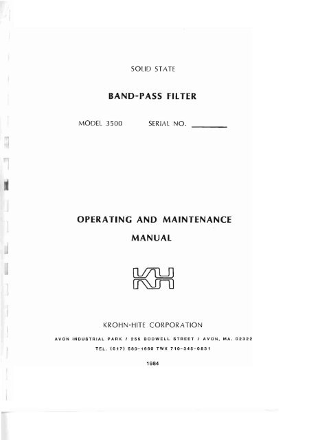
SOLID STATE<br />
BAND-PASS FILTER<br />
MODEL 3500<br />
SERIAL NO.<br />
OPERATING AND MAINTENANCE<br />
MANUAL<br />
KROHN-HITE CORPORATION<br />
AVON INDUSTRIAL PARK I 255 BODWELL STREET I AVON, MA. 02322<br />
TEL. (617) 580-1660 TWX 710-345-0831<br />
1984
Contents<br />
CONTENTS<br />
Section<br />
I<br />
2<br />
3<br />
4<br />
5<br />
6<br />
GENERAL DESCRIPTION<br />
OPERATION.<br />
CIRCUIT DESCRIPTION<br />
INCOMING ACCEPTANCE AND INSPECTION<br />
MAINTENANCE<br />
CALIBRATION AND ADJUSTMENT .<br />
Page<br />
I<br />
7<br />
9<br />
12<br />
15<br />
19<br />
ILLUSTRATIONS<br />
Figure<br />
I<br />
2<br />
3<br />
4<br />
5<br />
6<br />
7<br />
8<br />
9<br />
10<br />
I I<br />
Model 3500 Filter<br />
Normalized Frequency<br />
Square Wave Response<br />
Normalized Attenuation Characteristics<br />
Normalized Phase Characteristics<br />
Front <strong>and</strong> Rear Panels<br />
Simplified Schematic Diagram<br />
Test Point Voltages<br />
Top <strong>and</strong> Side View of Chassis<br />
Schematic Diagram<br />
PC307<br />
Page<br />
ii<br />
3<br />
4<br />
4<br />
5<br />
6<br />
9<br />
16<br />
18<br />
Foldout<br />
Foldout<br />
i
Filter 3500<br />
Model 3500<br />
. Figure 1. Model 3500 Filter<br />
ii
Section 1 - General Description<br />
SECTION 1<br />
GENERAL DESCRIPTION<br />
1.1 INTRODUCTION<br />
The Model 3500 Filter, shown in Figure 1, is a variable, electronic <strong>b<strong>and</strong></strong>-<strong>pass</strong><br />
<strong>filter</strong> that operates at frequencies from 20Hz to 200kHz. The <strong>filter</strong> consists<br />
basically of an input amplifier, a variable high-<strong>pass</strong> section, a variable low-<strong>pass</strong><br />
section, <strong>and</strong> an output amplifier. The high-<strong>pass</strong> <strong>and</strong> low-<strong>pass</strong> sections are connected<br />
in series. The overall gain of the Filter is unity(Odb). The cutoff frequencies<br />
of both the high -<strong>pass</strong> <strong>and</strong> low-<strong>pass</strong> sections can be adjusted independently over the<br />
full frequency range of 20Hz to 200kHz.<br />
An optional rack-mounting kit, (Part No. RK-38) is available from <strong>Krohn</strong>-<strong>Hite</strong>, for<br />
installing the unit in a st<strong>and</strong>ard 19" rack spacing.<br />
1.2 GENERAL SPECIFICATIONS<br />
Frequency Range<br />
Continuous coverage from 20Hz to 200kHz for both high cut-off <strong>and</strong> low cut-off frequencies<br />
independently. Frequency range is covered by separate calibrated dials<br />
<strong>and</strong> four-decade <strong>b<strong>and</strong></strong> switches. Center frequency <strong>and</strong> width of <strong>pass</strong> <strong>b<strong>and</strong></strong> in <strong>b<strong>and</strong></strong><strong>pass</strong>.<br />
mode are continuously adjustable over the entire frequency range.<br />
BAND MULTIPLIER FREQUENCY (Hz)<br />
1 1 20 - 200<br />
2 10 200 - 2, 000<br />
3 100 2, 000 - 20, 000<br />
4 lK 20, 000 - 200, 000<br />
Frequency Dials<br />
Each dial is engraved <strong>and</strong> individually h<strong>and</strong>-calibrated with a single logarithmic<br />
scale reading directly in cycles per second, from 19 to 210. Dials are 2 inches<br />
in diameter with an effective scale length of 6 inches per <strong>b<strong>and</strong></strong>, giving a total effective<br />
scale length of 24 inches for the range of 20Hz to 200kHz.<br />
Accuracy of Cut-off Frequency Calibration<br />
±10% with" Response" switch in" max-flat" (Butterworth) position; les s accurate in<br />
"Low QII position. Relative to mid-<strong>b<strong>and</strong></strong> level, the <strong>filter</strong> output is down 3db at cutoff<br />
in "max-flat" position, <strong>and</strong> approximately 12db in II Low Q" position.
Filter, 3500<br />
B<strong>and</strong>width<br />
Continuously v a r ia bl e within the cutoff frequency limits of 20Hz <strong>and</strong> 200kHz. For<br />
minimum <strong>pass</strong> -<strong>b<strong>and</strong></strong> (Butterworth response) the two cutoffs are set to the same<br />
frequency, resulting in an insertion los s of 6db at that frequency, with 3db points<br />
at factor s of .8 below it <strong>and</strong> 1. 25 above it.<br />
Response Characteristi cs<br />
Choice of 4 pole Butterworth (maximally flat response) for frequency domain operation<br />
<strong>and</strong> Low Q (damped response) for transient-free time domain operation, selected<br />
by means of a switch on rear of chassis.<br />
Pass-B<strong>and</strong> Gain<br />
Zero db ±l db in <strong>pass</strong> <strong>b<strong>and</strong></strong>.<br />
Input Characteri sti cs. Impedan ce<br />
Approximately 10 megohms in parallel with 50 pf. Maximum input amplitude:<br />
5 volts rms up to 2MHz. Maximum dc component: ]00 volts.<br />
Output Characteristics, Impedance<br />
Approximately 50 ohms. Maximum Voltage +7 volts peak. Maximum Current +5 rna<br />
peak. Internally generated hum <strong>and</strong> noise: L ess than 200 microvolts. (Slightly<br />
higher for 400 Hz operation. )<br />
Attenuation Slope<br />
Nominal 24db per octave each side of <strong>pass</strong>-<strong>b<strong>and</strong></strong>.<br />
Maximum Attenuation<br />
Greater than 60 db.<br />
Controls<br />
Front panel; LOW CUT-OFF FREQUENCY dial <strong>and</strong> multiplier switch. HIGH CUT<br />
OFF FREQUENCY dial <strong>and</strong> multiplier switch. POWER OFF-ON switch. Rear<br />
panel; RESPONSE switch, GROUND switch, 115/230V LINE switch.<br />
Terminals<br />
Front panel, two BNC connectors, one for INPUT <strong>and</strong> one for OUTPUT. Rear of<br />
chassis, two BNC connectors, one for input <strong>and</strong> one for output. An additional multipurpos<br />
e b inding post for CHASSIS GROUND is provided on the rear panel. An AC<br />
power receptacle with detachable line cord is also provid ed.<br />
Power Requ i rements<br />
105-125 or 210-250 volts, single phase; 50-400 Hz, 10 watts. Hum <strong>and</strong> noise<br />
are increased by a factor of approximately two for 400Hz operation.<br />
2
Section I - General Description<br />
Fuse Protection<br />
1/8 ampere slow-blow for 11 5 volts, 1/1 6 ampere slow-blow for 2 30 volts.<br />
Dimensions <strong>and</strong> Weights<br />
Model Overall Dimen sion s (inc hes) W e ig ht (lb s.)<br />
3500 8 1/2 wide I 3 1/2 high I 13 deep 9 net 114 shipping<br />
1.3 FILTER CHARACTERISTICS<br />
B<strong>and</strong>width Adjustment<br />
The flexibility of adjustment of <strong>b<strong>and</strong></strong>width is illustrated i n Figure 2. B<strong>and</strong>-<strong>pass</strong><br />
operation in the MAXimally FLAT or B utterworth m o d e for two different b arid ><br />
w i d t h s is illustrated by c u r v e s A <strong>and</strong> B. C u rve B s h ows the minimum p a ss -<strong>b<strong>and</strong></strong><br />
width obtained by setting the t wo c u t off f req u e nci e s equal. In this c o n d i t i o n the<br />
insert ion loss is 6 db, <strong>and</strong> the - 3 db cutoff frequencies o c c u r at 0. 8 <strong>and</strong> 1. 2 5<br />
times the m id- <strong>b<strong>and</strong></strong> frequency. The minimum pas s-<strong>b<strong>and</strong></strong> for a 0 db insertion los s<br />
is s h o w n by c u r v e A with the c u t offs s e t at 0.5 <strong>and</strong> 2 t ime s the mid - b a n d frequency.<br />
0<br />
-6<br />
-10<br />
:0<br />
::g -20<br />
z<br />
0 - 30<br />
~<br />
::::> -40<br />
z<br />
w<br />
I -50<br />
~ -60<br />
-70<br />
fI"<br />
...... A<br />
" "<br />
V 'I 8\ ,<br />
, 1\<br />
/ J If<br />
1\ '~,<br />
/ / \<br />
/ I 1\<br />
I V i'<br />
~<br />
~<br />
/ \<br />
1/ / \<br />
-80<br />
.01 .0 2 .04 .06 .1 .2 .4.6 2 4 6 10 20 40 60 100<br />
NORMALIZED FREQUENCY<br />
F igure 2.<br />
N orma l i z e d Frequency<br />
Transient Response<br />
The frequency r esponse c h a r act e r i s tic of this Filter closely approximates a fourthorder<br />
Butterworth with m a x im a l flatne s s , id e a l for <strong>filter</strong>ing in the frequency dom<br />
a i n. For puls e o r trans ient s i g n a l <strong>filter</strong>ing, a r e sponse swi tch is p r ovid e d to<br />
change the frequency re s ponse t o Low 0, optim u m for trans ient-free filte r ing.<br />
Figure 3 shows a comparison of t h e Filter output response in the se modes to a<br />
s q u a r e wave input signal.<br />
3
Filter, 3500<br />
(A)<br />
(E)<br />
Fig ure 3.<br />
Square Wave Re spon s e<br />
Cutoff Response<br />
The attenua tion cha r a cteristic s of the F ilter a re shown i n F i g u re 4. With t he<br />
r e sponse s w i t c h i n the MAXimally FLAT o r Butterworth m ode , the gain, a s shown<br />
by the solid c u rve , is virtually flat until the - 3db cutoff frequency. At approxim<br />
a t e l y two tim e s the cutoff frequency the attenuation rate coi n c id es w i t h t h e 24<br />
db per o ctav e straig h t line a s ymptote. In t he S impl e R C m ode, o ptimum for trans<br />
i e n t - f r e e fi lteri ng , the dot ted line s how s that the g a in i s down appro x imat el y 12<br />
db at cutoff <strong>and</strong> r e aches 2 4 db pe r octav e attenuation r ate a t five tim e s t he cut off<br />
f req u e ncy. Bey ond thi s frequency the <strong>filter</strong> attenuation r a t e a nd max i mum attenuation,<br />
in either m od e , ar e identi c al,<br />
o<br />
- 6<br />
- 12<br />
CD<br />
a<br />
~ - 18<br />
Section 1 - General Description<br />
Phase Response<br />
The phase angle at any frequency is the sum of the angle s due to the high-<strong>pass</strong> <strong>and</strong><br />
low-<strong>pass</strong> sections of the Filter. Figure 5 gives the phase characteristic for either<br />
section in degree s l e ad (+) o r lag (-), a s a function of the ratio of the <strong>operating</strong><br />
frequency f to low cut-off frequency f or high-cutoff frequency f H.<br />
L<br />
The solid curve i s for the maximally flat or Butterworth m ode <strong>and</strong> the dotted curve<br />
i s for Low Q.<br />
+360<br />
-- ....--- --;<br />
:::::--<br />
I<br />
+300 ·60<br />
<br />
• u ~<br />
u<br />
r\'<br />
o<br />
..J<br />
\.-',<br />
'" :I:<br />
+ 120 - 240<br />
~,<br />
""-'<br />
'r-...-... -, "<br />
+ 60<br />
~-~-----<br />
-- ---<br />
0"- t<br />
---<br />
~ ~ r ~ r<br />
t<br />
f%j<br />
t=:<br />
....<br />
(l)<br />
>-j<br />
-v.><br />
U1<br />
-<br />
0<br />
0<br />
FRONT VIEW<br />
REAR VIEW<br />
CD POWER SWITCH (ON / OFF)<br />
® INDICATOR LIGHT<br />
@ INPUT CONNECTOR (BNC TYPE)<br />
o OUTPUT CONNECTOR (BNC TYPE)<br />
® MULTIPLIER SWITCH (HIGH PASS)<br />
® MULTIPLIER SWITCH (LOW PASS)<br />
(!) FREQUENCY DIAL (LOW CUTOFF)<br />
® FREQUENCY DIAL (HIGH CUTOFF)<br />
® 115/230V LINE SWITCH<br />
@) OUTPUT CONNECTOR (BNC TYPE)<br />
® INPUT CONNECTOR (BNC TYPE)<br />
liSA SLO-BLO II7V<br />
@ 12 FUSE 1/16A SLO-BLO 234V<br />
@ POWER RECEPTACLE<br />
@ CHASSIS GROUND CONNECTOR (BINDING POST)<br />
@ GROUND SWITCH (FLOATING / CHASSIS)<br />
@ RESPONSE SWITCH (MAX FLAT / LOW Q)<br />
@ POWER TRANSFORMER<br />
@ NAMEPLATE<br />
FI GURE 6. FRONT AND REAR<br />
PANELS
Section 2 - Operation<br />
SECTION 2<br />
O PERATION<br />
2.1 INTRODUCTION<br />
The Filter i s adjusted <strong>and</strong> checked carefully before shipment t o insure that it meets<br />
all specifications. It is then aged <strong>and</strong> again tested to be sure that it is ready for<br />
use. The Filter is shipped complete, <strong>and</strong> after unpacking, is ready to be turned on<br />
<strong>and</strong> used.<br />
Unpack the Filter carefully <strong>and</strong> inspect it for damage that may have occurred during<br />
shipment. Check the case for damage, <strong>and</strong> check for loose sub-assemblies <strong>and</strong><br />
parts. Check all front panel controls for freedom of operation. The recommended<br />
<strong>operating</strong> procedure is described below .<br />
The r m s voltage of the input signal s h o u l d not exc e e d 5 volts.<br />
of the input signal should not exceed 100 v olts .<br />
The de component<br />
2.2 FRONT PANEL CONTROLS<br />
The front panel controls c o n s i s t of two identical frequency d ials <strong>and</strong> associated<br />
multiplier switches used to set cut-off frequencies, a power on-off switch, <strong>and</strong> an<br />
indicator light.<br />
Each frequency dial 1 S calibrated with a single logarithmic scale reading directly<br />
in cycles per second from 19 to 210. The dials are two inches in diameter with an<br />
effective scale length of approximately six inches per <strong>b<strong>and</strong></strong>, giving t o t a l effective<br />
scale length of approximately 24 inches for the 20Hz to 200kHz frequency range.<br />
The left-h<strong>and</strong> dial (LOW CUT-OFF FREQUENCY) <strong>and</strong> <strong>b<strong>and</strong></strong> multiplier switch select<br />
the low cut-off frequency, <strong>and</strong> the right-h<strong>and</strong> dial (HIGH CUT-OFF FREQUENCY)<br />
<strong>and</strong> multiplier switch select the h igh cut-off frequency.<br />
Each of the two multiplier switches has four positions, covering the frequency<br />
ranges as shown in Section 1. 2.<br />
2.3 REAR PANEL CONTROLS<br />
The r ear panel c o nt r o l s c o n s i s t of a RESPONSE switch, a GROUND switch, <strong>and</strong><br />
a 115/230V LINE switch. The RESPONSE switch is us ed to select either a<br />
Butterworth (max-flat) or a Low Q r esponse. The GROUND switch is provided<br />
to disconnect the signal ground from the chassis. The LINE switch i s used when<br />
changing from 115V to 2 30V AC operation.<br />
7
Filter, 3500 '<br />
2.4 OPERATION<br />
To operate the Filter, proceed as follows:<br />
a. Make appropriate power connections as described in Section 2.6.<br />
b. Make appropriate connections to INPUT <strong>and</strong> OUTPUT terminals of<br />
<strong>filter</strong>.<br />
c. Set cut-off frequencies by means of the <strong>b<strong>and</strong></strong> multiplier switches (CUT<br />
OFF FREQUENCY) <strong>and</strong> the frequency dials.<br />
d. Turn POW ER switch to ON.<br />
NOTE<br />
The left-h<strong>and</strong> <strong>b<strong>and</strong></strong> multiplier switch <strong>and</strong> frequency<br />
dial are used to select the low cut-off frequency<br />
<strong>and</strong> the right-h<strong>and</strong> controls select the high cut-off<br />
frequency.<br />
The minimum <strong>pass</strong> -<strong>b<strong>and</strong></strong> is obtained by setting the high cut-off frequency equal to<br />
the low cut- off frequency.<br />
2.5 TERMINALS<br />
INPUT - A BNC type connector is provided on the left side of the front panel. A<br />
parallel BNC coaxial connector is located on the rear of the chassis.<br />
OUTPUT - A BNC type connector IS provided on the right side of the front panel.<br />
A p a.r all e.l BNC coaxial connector is located on the rear of the chassis.<br />
CHASSIS GROUND - An additional combination-type binding post is provided on the<br />
rear panel.<br />
AC INPUT -<br />
rear panel.<br />
A power receptacle with detachable line cord is located on the<br />
2.6 LINE VOLTAGE AND FUSES<br />
The Filter may be operated from an AC power source of either 105-125 volts,<br />
50-400 Hz, or 210-250 vo lt s , 50-400 Hz. A 115/230V LINE s witch, located<br />
on the rear panel, selects the <strong>filter</strong>'s mode of operation. When the AC line is<br />
115V, mo ve the LINE switch to the 115V position. In this mode, a 1/8 ampere<br />
slo-blo fuse must be used. When the <strong>filter</strong> is to be operated from 230 VAC,<br />
move the LINE switch to the 230V position, <strong>and</strong> replace the fuse with a 1/16<br />
ampere slo-blo type.<br />
8
Section 3 -<br />
Circuit Description<br />
SECTION 3<br />
CIRCUIT DESCRIPTION<br />
3.1 INTRODUCTION<br />
As shown below in the simplified block diagram, Figure 7, the <strong>filter</strong> consists of an<br />
input amplifier, for isolation; a four pole low-<strong>pass</strong> section (high cutoff frequency),<br />
with four R. C. <strong>filter</strong> networks which are adjustable by means of a gauged potentionmeter<br />
assembly <strong>and</strong> <strong>b<strong>and</strong></strong>switch; <strong>and</strong> a four pole high <strong>pass</strong> section (low c u t o ff frequency),<br />
with four R. C. <strong>filter</strong> networks <strong>and</strong> a similar ganged potentionmeter assembly<br />
<strong>and</strong> b <strong>and</strong> s wit c h, Both cutoff frequencies are tuned continuously within each<br />
decade by the potentionmeter assemblies. The capacitors are tuned in decade steps<br />
by the <strong>b<strong>and</strong></strong> s wit ch,<br />
INPUT<br />
r>: ~ f-
Filter, 3500<br />
3.2 DETAILED DESCRIPTION<br />
3.2.1 Input Amplifier<br />
The input signal i s c apacitor coupled through CIO I to the input a m plifie r cons i sting<br />
of Q 10 1 <strong>and</strong> Q 102 0 The input impedance determined by RI O1 is 10 megohms . The<br />
h ig h input impedance of t he F. E. T. QI O1 is negligible. The input a mplifier i s<br />
provided to isolat e the input signal <strong>and</strong> s upply a low impedance d riving s o u rce for<br />
the fir st R. C. network.<br />
3.2.2 High Pass Section<br />
The high <strong>pass</strong> section consists of a pair of two pole <strong>filter</strong>s, each a d j ust e d to provide<br />
the proper Butterworth response characteristics when cascaded. Buffer amplifiers<br />
are used to isolate the two pole R. C. networks. The Buffer Amplifier,<br />
consisting of Q20 1 <strong>and</strong> Q202, folIowing the first 2 pole network provides isolation<br />
<strong>and</strong> drives the next R. C. network. Q203 furnishes feedback to the emitter follower<br />
stage for corner frequency peaking. The signal then enters another Buffer Arnpli »<br />
fier stage consisting of Q204 <strong>and</strong> Q205, again providing i s ol a t i o n <strong>and</strong> a low impedance<br />
source to drive the next R. C. n etwork. Q206 <strong>and</strong> Q207 perform as a buffer<br />
amplifier between the high-<strong>pass</strong> <strong>and</strong> low-<strong>pass</strong> sections with Q20 8 providing enough<br />
feedback to Q204 to produce the correct Butterworth response. With s witch 5901<br />
in the grounded position, the feedback is reduced to produce the Low Q (damped<br />
response) for transit free time domain operation.<br />
3.2.3 Low Pass Section<br />
The low <strong>pass</strong> section also consists of a pair of two pole <strong>filter</strong>s each adjusted to<br />
provide the proper Butterworth response when cascaded.<br />
The pair of two pole R. C. networks are isolated from each other with a buffer<br />
amplifier which is made up of two emitter followers .<br />
The output from the high-<strong>pass</strong> section is fed into the first two-pole R. C. network<br />
before the buffer amplifier consisting of 0301 <strong>and</strong> Q302. A portion of the output<br />
from 0302 i s fed back to the R. C. network v i a Q303 to obtain the de sired characteristics<br />
from this two pole section. The buffer amplifier also provides a low<br />
impedance s o u r c e for driving the next pair of R. C. <strong>filter</strong>s. Q304 <strong>and</strong> Q305 provide<br />
isolation <strong>and</strong> a low impedance source to drive the output. A portion of the output<br />
from Q305 is fedback through amplifier Q306 to obtain the proper Butterworth<br />
response characteristics. With s w i t c h 5901 in the grounded position the feedback<br />
is reduced to a low Q (damped re s p ons e) for transit free time domain operation.<br />
The output from Q305 <strong>pass</strong>es through C303 <strong>and</strong> R411 to the output terminals.<br />
3.2.4 RC/Butterworth Response<br />
To prevent ringing <strong>and</strong> overs hoot, caused b y fast rise-time pulses, the <strong>filter</strong> may<br />
be operated in the low Q position. 5901 is provided to reduce the feedback to the<br />
second two pole <strong>filter</strong> in each section.<br />
10
Section 3 - Circuit Description<br />
3.2.5 Power Supplies<br />
A dual power supply i s incorporated. providing plus <strong>and</strong> minus 15 volts. One full<br />
wave bridge rectifier (CR501,.CR504, CR505, CR506) <strong>and</strong> <strong>filter</strong> cap a cit o r s C501 <strong>and</strong><br />
C50Z provide the necessary un r e g u Iat e d d- c v oltage l evels.<br />
The + I5V supply consists of 0502 (used as a Zener R eference), amplifier 0503,<br />
<strong>and</strong> series regulator 0501. A c h a ng e in the regulated output is fed through 0502<br />
<strong>and</strong> CR502 to the e m it t e r of 0503, <strong>and</strong>, attenuated in the divider R511 <strong>and</strong> R 501,<br />
R506, to the base of 0 503. The resulting change in 0503 c u r ren t drives the base<br />
of series transistor 0501 in the proper direction to r estore the regulated v olta g e<br />
to + 15V. The -15V supply works in the same manner.<br />
Additional feedback is provided to both amplifiers via R505 <strong>and</strong> R50 8 to minimize<br />
power supply ripple.<br />
J<br />
J<br />
II
Filter, 3500<br />
SECTION 4<br />
INCOMING ACCEPTANCE AND INSPECTION<br />
4.1 INTRODUCTION<br />
The following procedure should be used to verify the Filter operation within specifications.<br />
These checks may be used for incoming inspection <strong>and</strong> periodic specification<br />
checks. Tests must be made with all covers in place. If the instrument is not<br />
<strong>operating</strong> within specifications refer to Section 5 before attempting any detailed<br />
<strong>maintenance</strong>.<br />
4.2 TEST EQUIPMENT REQUIRED<br />
The following test equipment is required to perform these adjustments:<br />
a. RC Oscillator, with frequency range. OlHz to lMHz, frequency<br />
accuracy +0. 5% to 100KHz, frequency response better than +. 05db<br />
<strong>and</strong> distortion less than. 02%, <strong>Krohn</strong>-<strong>Hite</strong> Model 4100A or equivalent.<br />
b. Oscilloscope, with DC to 50MHz <strong>b<strong>and</strong></strong>width, vertical input sensiti<br />
vity of lmv/cm, Tektronix type 544, with type lA5 plug-in, or<br />
equivalent.<br />
c. AC Voltmeter, capable of measuring 100 microvolts to 10 volts<br />
RMS, Ballantine Model 3l4A or equivalent.<br />
d. DC Voltmeter, capable of measuring I millivolt to 20 volts, Fluke<br />
Model 8000A or equivalent.<br />
j<br />
e. Variable auto-transformer for adjusting line voltage.<br />
4.3 DIAL ACCURACY<br />
a. Set high cutoff to 200KHz. Set re s p ons e switch to max flat pos i t i o n . Set<br />
low cutoff dial to 20, 40, 100, 200 on each of the multiplier positions. At each point,<br />
set oscillator to frequency corresponding to dial <strong>and</strong> multiplier setting. With 1 volt<br />
input, output should read between O. 6V <strong>and</strong> O. 8V (-3db±1. 5db) at all frequencies<br />
e xcept 200KHz will read approximately 0.5 volts (-6db) due to interaction of high<br />
cutoff setting.<br />
b. Repeat measurements with response switch in low Q position. Output reading<br />
should be approximately 0.25 volt s (-12db) at all frequencies except 200 KHz.<br />
12
Section 4 - Incoming Acceptance <strong>and</strong> Inspection<br />
c. Set low cutoff to 20Hz. Set response switch to max flat position. Set high<br />
cut off dial to 20, 40, 100, 200 on each of the multiplier positions. At each point,<br />
set oscillator to frequency corresponding to dial <strong>and</strong> multiplier setting. With 1 volt<br />
input, output should read between 0.6V <strong>and</strong> O. 8V (-3db±1. 5db) at all frequencies<br />
except 20 Hz. 20Hz will read approximately O. 5V (-6db) due to interaction of low<br />
cutoff frequency.<br />
d. Repeat measurements with response switch in Low Q position. Output reading<br />
should be approximately O. 25V (-12db) at all frequencies except 20Hz.<br />
4.4 ATTENUATION SLOPE<br />
a. Set high cutoff to 200 KHz <strong>and</strong> response switch to max flat position. Set<br />
low cutoff dial to 60. On each low cutoff multiplier position set oscillator to one<br />
half the frequency indicated by the low cutoff dial <strong>and</strong> multiplier setting. Output<br />
should read -24db±3db from input at each frequency.<br />
b. Set low cutoff to 20Hz. Set high cutoff dial to 60. On each high cutoff multiplier<br />
position, set oscillator to twice the frequency indicated by the high cutoff dial<br />
<strong>and</strong> multiplier setting. Output should read -24db±3db from input at each frequency.<br />
4.5 PASS-BAND GAIN<br />
Set low cutoff to 20Hz <strong>and</strong> high cutoff to 200KHz. Set oscillator to 1 volt. At 50 Hz,<br />
500 Hz, 5 KHz <strong>and</strong> 50 KHz the output should be 1±. 1 volt (Odb±1db).<br />
4.6 MAXIMUM ATTENUATION<br />
a. Set both cutoff frequencies to 200KHz. Set oscillator input to <strong>filter</strong> at<br />
5 volts, 20KHz. Output of <strong>filter</strong> should measure less than 5 millivolts (-60db).<br />
J<br />
b. Set both cutoff frequencies to 20KHz. Set input to <strong>filter</strong> to 5 volts, 200KHz.<br />
Output of <strong>filter</strong> should measure less than 5 millivolts (-60db).<br />
4.7 OUTPUT CHARACTERISTICS<br />
a. Maximum Voltage:<br />
Set low cutoff to 20Hz <strong>and</strong> high cutoff to 200KHz. Set input frequency to<br />
1KHz <strong>and</strong> increase input voltage until clipping is observed on output. Output should<br />
measure greater than 14 volts peak to peak before clipping is observed.<br />
b. Maximum Current:<br />
Connect 50 ohm resistor across output. Adjust input to obtain 0.5 volts<br />
peak to peak across 50 ohm resistor. Output should show no observable distortion.<br />
13
Filter, 3500<br />
c. Impedance:<br />
Set output to O. 1 v olt rms open circuit. Connect 50 ohm resistor to output.<br />
Voltag e should drop to 0. 05 v olt s .<br />
4.8 HUM AN D NOI SE<br />
R emove oscillator. Short i np u t to <strong>filter</strong>. Output should measure les s than<br />
2 00 microvolts rms.<br />
14
Section 5 - Maintenance<br />
SECTION 5<br />
MAINTENANCE<br />
5.1 INTRODUCTION<br />
If the Filter is not functioning properly <strong>and</strong> requires service, the following procedure<br />
may facilitate locating the source of trouble. Access to the interior of the <strong>filter</strong> is<br />
accomplished by removing the four screws centered at the rear of each cover; sliding<br />
off the side covers will unlock the top <strong>and</strong> bottom covers.<br />
The general layout of major components, test points, screwdriver controls <strong>and</strong> adjustments<br />
is shown in Figure 9. Detailed component layout of the printed circuit<br />
card, Figure II, is located on foldout attached to the inside rear cover. Various<br />
check points <strong>and</strong> voltages are shown on the Schematic Diagram <strong>and</strong> are also marked<br />
on the printed circuit card.<br />
Many troubles may easily be found by visual inspection. When a malfunction is detected,<br />
make a quick check of the unit for such things as broken wires, burnt or<br />
loose components, or similar conditions which could be a cause of trouble. Any<br />
trouble-shooting of the Filter will be greatly simplified if there is an underst<strong>and</strong>ing<br />
of the operation of the circuit. Before any detailed troubleshooting is attempted,<br />
reference should be made to Circuit Description, Section 3, to obtain this<br />
underst<strong>and</strong>ing.<br />
5.2 POWER SUPPLY<br />
If the <strong>filter</strong> does not seem to be working properly the two power supplies should be<br />
checked first. If the plus 15 <strong>and</strong> minus 15 volt supplies appear to be correct refer<br />
to signal tracing analysis, Section 4.3.<br />
Any malfunction of the power supplies will generally cause a large error in the plus<br />
or minus 15 volt supplies. Small errors of the plus or minus supplies may be corrected<br />
by adjusting R506 <strong>and</strong> R509 respectively. If the minus 15 volt supply is correct<br />
<strong>and</strong> the plus 15 volt supply is incorrect, check the reference voltage from the<br />
emitter of 0503 to the collector of 0502. If this reference voltage is 8. 4±. 5 <strong>and</strong> the<br />
plus 15 volt supply is high, the base to emitter voltage of 0503 will be reduced, decreasing<br />
its collector current lowering the emitter to base voltage <strong>and</strong> turning off<br />
0501. This will increase the emitter to collector voltage of 050 I, correcting the<br />
plus 15 volt supply. The failure will be found where this action is blocked. If the<br />
plus 15 volt supply is low, the current in 0503 will be increased, turning on 0501.<br />
If the supply voltage is low <strong>and</strong> 0503 <strong>and</strong> 0501 appear to be <strong>operating</strong> properly, the<br />
cause is most likely excessive current in the main <strong>filter</strong> section. An incorrect minus<br />
15 volt supply may be traced in a similar manner.<br />
15
Filter, 3500<br />
5.3 SIGNAL TRACING ANALYSIS<br />
If the power supplie s appear to be correct but the Filter is not working, the following<br />
signal tracing analysis should locate the area of malfunction:<br />
Set response switch to low Q p o s i t i o n , Set both the low <strong>and</strong> h ig h cutoff frequencies<br />
to 1KHz. C onnect a 1K H z 5 volt rms sine wave signal to the input terminal s. If<br />
the test s ign a l does not appear correctly at the output, the area of the malfunction<br />
may be localized by determining where in the Filter the signal first deviates from<br />
normal.<br />
Figure 8 s h o w s various test points with<br />
their correct signal levels. If a test point<br />
i s found whose s ignal level differs appreciably<br />
from the correct value, the circuitry<br />
immediately preceding that test point<br />
should be carefully checked.<br />
5.4 TUNING CIRCUITS<br />
If signal tracing shows one of the tuning<br />
circuits to be faulty, it should be determined<br />
i.f the trouble is in the resistive or capacitive<br />
element. If the trouble is in a capacitive<br />
element associated with the lowest or<br />
highe st multiplier range, the malfunction<br />
will appear only on these positions. Any<br />
other defective tuning capacitors will introduce<br />
an error in adjacent <strong>b<strong>and</strong></strong>s. If there<br />
is a problem in a resistant element, the<br />
trouble will be of a general nature <strong>and</strong> will<br />
show up on all multiplier <strong>b<strong>and</strong></strong>s.<br />
TEST POINTS<br />
CORRECT<br />
SIGNAL LEVEL<br />
(RMS VOLTS)<br />
I 5.0<br />
2 4.9<br />
3 2.8<br />
4 2.8<br />
5 2.6<br />
6 1.6<br />
7 1.6<br />
8 1.3<br />
10 1.3<br />
13 .43<br />
14 .70<br />
15 .67<br />
16 • 18<br />
17 · 31<br />
18 .30<br />
20 · 14<br />
The range-determining capacitors as- Figure 8. Test Point Voltages<br />
sociated with the <strong>b<strong>and</strong></strong> multiplier switches<br />
S701 <strong>and</strong> S702 are specially selected for<br />
close capacitance tolerance. All capacitor<br />
values fall within ±5% of the specified value, but in order to maintain accurate<br />
frequency calibration over the entire dial range <strong>and</strong> also between decade ranges, the<br />
capacitors are matched within ±2% of each other <strong>and</strong> generally within ±2% in decade<br />
ratios.<br />
The values of capacitance used on the highest <strong>b<strong>and</strong></strong> is selected to compensate for<br />
stray capacitance <strong>and</strong> are therefore not completely in decade ratios of those used<br />
on the lower <strong>b<strong>and</strong></strong>s.<br />
For replacement purposes, a capacitor within ± 1% of the specified value can be<br />
used with negligible effect on the overall calibration accuracy. If more than one<br />
capacitor on a particular range is to be changed, it is recommended that several<br />
other capacitors on the switch be carefully measured on a capacitance bridge to<br />
determine the average percentage deviation from the nominal value. Any capacitors<br />
e xcept those used on the two highest frequency ranges may be measured to determine<br />
16
Section 5 -<br />
Maintenance<br />
this tolerance. Replacement can then be made with capacitors of the exact value,<br />
<strong>and</strong> calibration will not be impaired.<br />
Each of the variable resistance elements consists of four potentiometers ganged<br />
together with a g e a r assembly. Each potentiometer has series <strong>and</strong> shunt trims to<br />
insure proper tracking. The trims <strong>and</strong> the angular orientation of the potentiometers<br />
are carefully adjusted at the factory. If it becomes nece s sary to change one of<br />
these potentiometers in the field, it should be replaced only with a unit supplied by<br />
the factory complete with proper trims. The angular orientation should then be<br />
carefully adjusted following the procedure supplied with the parts.<br />
17
Filter, 3 50 0<br />
CI02 C707 R702 C717 C741<br />
o +<br />
'"<<br />
C727<br />
\ /<br />
I \ /<br />
I \ /<br />
-U t~J~~<br />
C737<br />
I<br />
I<br />
S IDE VIEW<br />
FI GURE 9. TOP AND SIDE VIEW OF<br />
CHASSIS<br />
18
Section 6 - Calibration <strong>and</strong> Adjustment<br />
SECTION 6<br />
CA LI BRATIO N AND AD JUSTM ENT<br />
6.1 INTRODUCTION<br />
Before attempting any adjustments the procedure in Section 4 should b e followed to<br />
determine if adjustments are n ecessary. The following procedure is provided for<br />
the purpose of facilitating the adjustment <strong>and</strong> calibration of the <strong>filter</strong> in t he field,<br />
<strong>and</strong> adherence to thi s procedure should re store the <strong>filter</strong> to its original specifications.<br />
If any difficultie s are encountered, please refer to Maintenance, Section 5.<br />
1£ any questions arise w h i c h are not covered by this procedure, please contact our<br />
factory service department. The location of all major components, m od ul a r subassemblies,<br />
test points, screw driver controls <strong>and</strong> adjustments are shown in<br />
Figure 9.<br />
Access to t he interior of the <strong>filter</strong> is accomplished easily by removing the four<br />
screws centered at the rear of each cover; sliding off the side cover s will unlock<br />
the top <strong>and</strong> bottom cover s ,<br />
6.2 TEST EQUIPMENT REQUIRED<br />
AS LISTED IN SECTION 4.2<br />
6.3 INITIAL SETUP<br />
a. Set low cutoff dial to 60, multiplier to x l O;<br />
b. Set high c u t o ff dial to 200, multiplier to x l K.<br />
6.4 POWER SUPPLY<br />
a. Short <strong>filter</strong> input. Connect d- c voltmeter betwe en signal ground<br />
a n d plus 15 v olts . (positive e n d , C505 )<br />
b. Adjust R 5 06 for 15+ 0.2 v o lts .<br />
c. Connect d-c voltmeter between signal ground <strong>and</strong> minus 15 volts.<br />
(n e gativ e end of C 5 06 )<br />
d. A djust R509 for 15+ 0.2 volts.<br />
e. R e move short.<br />
19
F ilte r, 3500<br />
6.5 LOW·CUTOFF SECTION RESPONSE<br />
a .<br />
C onnect o scillator ou t pu t to <strong>filter</strong> input.<br />
b .<br />
Set o s c illator t o 6 KHz <strong>and</strong> a dju s t amplitude for 1 v o lt a t<br />
<strong>filter</strong> input.<br />
c . Connect AC vo ltm e ter to p o i nt " 10" .<br />
d. Adjust R226 fo r reading of IV, +.02V<br />
e . Set o scilla t o r to 6 0 0H z .<br />
f. Adjust R225 for a reading of . 7 v olts a t point " 10" .<br />
6.6 LOW-CUTOFF DIAL SETTING<br />
a .<br />
Set oscillato r frequency to 3 KHz.<br />
b . A djust voltage for 1 volt at p o int " 10 " .<br />
c .<br />
S e t oscillator to 300 Hz.<br />
d . Adjust low cutoff dial for . 063 volts (-24db from 1 volt ) at point "10" .<br />
e . If nece ssary, loosen dial set screws <strong>and</strong> set dial at 60.<br />
6.7 LOW CUTOFF Xl K MULTIPLIER CALIBRATION<br />
6.7.1 Step 1<br />
a . Set l ow c ut o ff dial t o 20, multiplier to x l K ,<br />
b. Set oscillator to 10 0K H z <strong>and</strong> connect AC voltmeter to p o i n t " 4" .<br />
c. Adjust v olta g e at p oint "4" for 1V r rn s ,<br />
d. Swit c h oscillator t o 5KHz.<br />
e . Adjust C 7 07 for . 06 v olts (-24. 5db f rom 1 volt) at p o i nt " 4" .<br />
f. Repeat s t e p s b throug h f until no additional adjustment i s required.<br />
20
Section 6 - Calibration <strong>and</strong> Adjustment<br />
6.7.2 Step 2<br />
a . Set oscillator to 100KHz <strong>and</strong> connect AC voltmeter to point" 10".<br />
b. Adjust voltage at point" 10" for I v olt r rn s ,<br />
c. Switch oscillator to 10KHz .<br />
d . Adjust C717 for. 063 volts (-24db from 1 v olt) at point "10".<br />
e. Repeat steps a through e until no additional adjustment is required.<br />
6.8 200KHZ CALIBRATION<br />
a. Set low cutoff dial to 200, multiplier to x l K,<br />
b. Set oscillator to 600 KHz.<br />
c. Adjust oscillator for 1 v olt at point" 10".<br />
d. Switch oscillator to 200KHz.<br />
e. Trim C741 for O. 7±. 05 v olts at point" 10".<br />
6.9 HIGH CUTOFF DIAL SETTING<br />
a .<br />
Set low cutoff dial to 20, multiplier to xl.<br />
b. Set high cutoff dial to 60, multiplier to x l O,<br />
c. Set oscillator frequency to 100 Hz.<br />
d. Adjust oscillator voltage for 1 volt at <strong>filter</strong> output.<br />
e. Switch oscillator to 1. 2 KHz.<br />
f. Adjust high cutoff dial for. 063 volts (- 24 db from 1 volt) at output.<br />
g. If necessary, loosen dial set screws <strong>and</strong> set dial at 60.<br />
6.10 HIGH CUTOFF X1 K MULTIPLIER CALIBRATION<br />
a. Set high cutoff dial to 60, multiplier to x l K,<br />
b. Set oscillator to 6 KHz.<br />
21
Filter, 3500<br />
c .<br />
Adjust oscillator voltage for 1 volt at <strong>filter</strong> output.<br />
d. Switch oscillator t o 4 8KHz.<br />
e .<br />
Adj u st C727 for a r eadin g of . 94 volts a t <strong>filter</strong> output.<br />
f. Switch oscillator to 6 0 KHz .<br />
g .<br />
Adjust C737 for a r eading of O. 7±.. 05 volts a t filte r output.<br />
h . Repeat steps d through g u ntil no further adjustment is r e qu ire d .<br />
22
I<br />
' 1l'V1(T<br />
~T ' : ,1<br />
~ , v ~ '<br />
I I '" c!:'J -r-' .<br />
I ' I I<br />
t.il<br />
,1;. ~ : ~ .P<br />
'-...... Y.<br />
AEAR<br />
I NPUT<br />
r -- - - - - - - - - - - - ~<br />
I<br />
I<br />
I<br />
I<br />
I<br />
I<br />
I<br />
I<br />
,<br />
C'W1 1',<br />
1* ' .:<br />
::U<br />
,....<br />
It~ , ,1<br />
.00<br />
1 - - - - - - - - - - - - - - - _. - - - . ~ . - . - - - - - -- -<br />
~<br />
-I'"<br />
1'15'"<br />
,, ~<br />
1.1)1<br />
- H I<br />
J ••<br />
~ t:<br />
"<br />
t !llll<br />
t.:-.I<br />
: ~ ~<br />
+"" f!<br />
·/I~ · S ~ i : n<br />
; .t" _~.: (<br />
1.:::::.- -.E~f , ..... ' ~ - - ".<br />
~' .~ ~ - - : ~<br />
G:0 1 "J<br />
. i : ~ T ~ , ,~<br />
-"'E j I I : I I I l I. . I I I ! .. 1 I I " I<br />
" ~ ' I<br />
~ .) l<br />
" 1.'<br />
t. tt<br />
.... L :la<br />
'"<br />
· Ul<br />
1~~ '<br />
3 ~ - - - - - -<br />
I ~<br />
I<br />
I<br />
I<br />
I<br />
I<br />
I<br />
I<br />
I<br />
I<br />
L- -1-<br />
.. ~ I _ l l . ·~<br />
~ .---~<br />
c·n ~ ! "<br />
~ f/'J'- "~ r,' t -L;J - ri i'll:<br />
L ~ __ ~l~~ -1 ---l.. __ ...:.!2.!. ~ ~!....- -l<br />
LOW CUT OFF<br />
FRE QUEN CY T UN IN G<br />
.,,,<br />
' II<br />
,.<br />
' l '<br />
,f"<br />
r<br />
I<br />
o 51tr<br />
, 11f<br />
",.<br />
" <br />
.Il<br />
//<br />
~<br />
0 \<br />
"I<<br />
o<br />
~ H<br />
1"'1 "" '.1'<br />
...<br />
,.,. j<br />
..... ~ I LOW<br />
FL.ATcf~<br />
,RESPONSE -r<br />
SWITCH<br />
- - - - - - - - - - - - - - - - - - - ~1~14 ~.I~n-;~ -;A;f'I::J,J-;VI - - - - - - - - - - - - - - - - - -.. - - - l<br />
nOlA<br />
G<br />
I<br />
I<br />
I<br />
I<br />
~<br />
I<br />
;:;:< I I<br />
I<br />
I<br />
"U<br />
FRom<br />
OUTPUT<br />
~ ~ ,<br />
fl<br />
L....+- j I ==--".I L"""",,,-, I, j j . uv<br />
NOTES<br />
AL L RESI STORS l ~ OHMS UNLE SS<br />
OT ME RWI 5E SPEC IFIE D.<br />
n i<br />
•-r<br />
.n :<br />
. r,<br />
-"'-II It-I I II l~ ~W<br />
- -- ~..=--~--<br />
- ~" ~~ \<br />
. ~.<br />
t . ~ •<br />
---<br />
- --<br />
:: ~ I<br />
REAR<br />
OUT1'
~ ES ls r ORJ<br />
-<br />
5"..m1 Dr:" \.Crip, iOl' . ",Jt. P~t Nc ,<br />
Sr ;r.t.:..tl Of!' \CTipti '='tl tlf, . Po" !'fo.<br />
")~ Ill: i ' · ... ·<br />
R. l 0 1 10" lO';.g 1/4·..' .... CB1061 R31:'J<br />
I ",SK 10 • I/ "W A! " ami<br />
k lOI ' M 10 ' u...., AI CRIOS I<br />
RJI:I J.n s. ,/ .cw 1.6 CI3925<br />
k lOJ 100 10'1 1/ ' 1': AI C810 11<br />
RJI' 100 II. ",<br />
M CBI012<br />
RIO' H'. 10' 1/ "": AI CBIOIl p.J 5<br />
" i"'J 20' , 1/• ••• AI 112<br />
RIOS .; 1(> I /:. '/.· ~I CMOlI<br />
' 31'J JV<br />
TIlW X663f<br />
C801 6. 8pf 10",-0 SOOV ASP 92 12- 68910<br />
- 3 ~ .<br />
0 12<br />
Iml .,.,.-. lOOV TRW Xb6Jf<br />
-310<br />
TRANSISTO RS. DIODES. MISC.<br />
Symbol Delc ripriol'l<br />
Mfr . Port No. Sy.....1<br />
DCic.ription<br />
Mfr . Part N Cl.<br />
0'0 1<br />
2N4 302<br />
AME 2N4302<br />
0 102<br />
MPSOS I8<br />
MOT MP56Sl8<br />
L201 FERRITE 8EAD<br />
STK S7-0 181<br />
1.301<br />
luH y IlK 1/4W<br />
DLV 1537-12<br />
0 201 Ml'S6SIS MOT Ml'S6SlS<br />
l302<br />
l uHy 10% 1/4W DLV ISJ7- 12<br />
l3l3<br />
l url y IO"~ I/. w , 'Z'N A. J9S128<br />
0205 MP56518<br />
MOT MP56518<br />
P602<br />
15K I ~~ 7:" A. J9321l0D<br />
0206 2N4 3C2 AME. 2N'302 P603<br />
90K lit ~ : I A. » sra<br />
0207 ,..\P$~ I B MOT MP 5o-J~ I B<br />
P604<br />
90K ,0'>. z.," i A. .fI , T17<br />
0 208 MP56S16<br />
,,",O T MP56S15<br />
P60S<br />
25K 10" 7:'/ I A. J9J 2I3OD<br />
P6Q6 250K 10 LC, i A_ Jhn e<br />
0 301 MP$ ~5 ) S MO r MP'S65 S<br />
P607<br />
90K 10 'Zoo', A. .1I,j72 7<br />
0 :SI8<br />
MOT Mi' 565 18<br />
O :>JS 2NS I89 RCA 2N 5 189<br />
5701<br />
SWITCH. ROTARY KH 8-2657/C<br />
0S06 .V PSb·~<br />
MOT MP53'>40<br />
S702<br />
SWITCH, ROTARY KH B-2657/C<br />
CR4QI IN41. 9<br />
TR IN. 149<br />
5901<br />
SWITCH. Sl iDE CW G- '26<br />
S902<br />
SWITCH, SLIDE CW GF- 123<br />
CRSOI IN 4.:n MSC IN400 2<br />
5903<br />
SWITCH, SLIDE<br />
SWC 16 256LFR<br />
CRS02 M.Z2361 MOT M.Z2J61<br />
5904<br />
SWITCH, TO G GLE CK Ull<br />
CRS03 M.Z 2361<br />
MOT M.Z2361<br />
CRS04<br />
IN4::' 1D2<br />
MSC IN4oo2<br />
CRSOS<br />
1N4002<br />
MSC IN4002 T901<br />
TRAN Sf O RMER. POWER KH 8--2653/E<br />
CRS06<br />
INl002<br />
MSC IN4002<br />
I
','1. Vi e w, Calif.<br />
O~!Y.l ; ~ , P.1.<br />
MilwouM OO'l , W i, e ,<br />
St. Louh, 1/'1..1.<br />
N . wor:':' , N , J.<br />
'.' ,' 1I.. etc ....",. I" ' '':U~.<br />
F1I il~ .; .. jp"i' J, P; .<br />
t o31 l l\ urc m , N . ...<br />
COtnptOO , Cl.Ilif.<br />
'<br />
ELM 1721 :161<br />
Ell !72982,<br />
Mo r 10m 3)<br />
MSC<br />
RCA 1496111<br />
\ P ' \ b2 ~<br />
sr-,<br />
~ 1 34 88<br />
r p. ilJJ,8,"n<br />
r RW (8+4 11'<br />
E" le