

Surface-enhanced Raman scattering of rhodamine ... - ResearchGate
Surface-enhanced Raman scattering of rhodamine ... - ResearchGate
Surface-enhanced Raman scattering of rhodamine ... - ResearchGate

Create successful ePaper yourself
Turn your PDF publications into a flip-book with our unique Google optimized e-Paper software.
IOP PUBLISHING<br />
Nanotechnology 19 (2008) 275712 (5pp)<br />
NANOTECHNOLOGY<br />
doi:10.1088/0957-4484/19/27/275712<br />
<strong>Surface</strong>-<strong>enhanced</strong> <strong>Raman</strong> <strong>scattering</strong> <strong>of</strong><br />
<strong>rhodamine</strong> 6G on nanowire arrays<br />
decorated with gold nanoparticles<br />
Jianing Chen 1,2 ,ThomasMårtensson 3 , Kimberly A Dick 3 ,<br />
Knut Deppert 3 ,HQXu 1,3 , Lars Samuelson 3 and Hongxing Xu 2,3<br />
1 School <strong>of</strong> Physics and Optoelectronic Technology, Dalian University <strong>of</strong> Technology,<br />
Dalian 116024, People’s Republic <strong>of</strong> China<br />
2 Beijing National Laboratory <strong>of</strong> Condensed Matter Physics, Institute <strong>of</strong> Physics, Chinese<br />
Academy <strong>of</strong> Sciences, Beijing 100190, People’s Republic <strong>of</strong> China<br />
3 Division <strong>of</strong> Solid State Physics, Lund University, S-22100 Lund, Sweden<br />
E-mail: hxxu@aphy.iphy.ac.cn<br />
Received 5 March 2008, in final form 5 May 2008<br />
Published 28 May 2008<br />
Online at stacks.iop.org/Nano/19/275712<br />
Abstract<br />
We investigate the surface-<strong>enhanced</strong> <strong>Raman</strong> <strong>scattering</strong> (SERS) <strong>of</strong> <strong>rhodamine</strong> 6G (R6G)<br />
adsorbed on Au nanoparticles attached to InP nanowires. We find that nanowire arrays act as<br />
frameworks for effective SERS substrates with a significantly higher <strong>Raman</strong> signal sensitivity<br />
than a planar framework <strong>of</strong> Au nanoparticles adsorbed two-dimensionally on a flat surface. The<br />
SERS signal displays a clear polarization-dependent effect when the nanowires are arranged in<br />
a row. We also find that the SERS signal increases with time during continuous laser<br />
illumination. The plasmon-<strong>enhanced</strong> optical forces between Au nanoparticles may either move<br />
pairs <strong>of</strong> nanoparticles closer together or attract adsorbed molecules by moving them to the<br />
junctions <strong>of</strong> Au nanoparticle aggregates. Such effects by plasmon optical forces may cause the<br />
observed increase <strong>of</strong> the SERS signal with continuous laser illumination.<br />
1. Introduction<br />
<strong>Surface</strong>-<strong>enhanced</strong> <strong>Raman</strong> <strong>scattering</strong> (SERS) was first reported<br />
more than 30 years ago by Fleischmann et al [1] and Jeanmaire<br />
and Van Duyne [2], and is now widely used to acquire <strong>Raman</strong><br />
signals from small quantities <strong>of</strong> molecules, even down to<br />
the single-molecule level. Because <strong>of</strong> its high sensitivity,<br />
SERS has developed into an important spectroscopic tool<br />
in many fields [3–6]. It is generally believed that the two<br />
mechanisms that contribute to SERS are electromagnetic (EM)<br />
enhancement [7, 8] and chemical enhancement [9, 10]. For<br />
the EM mechanism <strong>of</strong> enhancement, the SERS intensity can<br />
be <strong>enhanced</strong> substantially when two or more nanoparticles are<br />
brought closely together [6, 7]. The small areas or cavities<br />
formed between those closely neighbored nanoparticles are<br />
called ‘hot’ sites, where the <strong>Raman</strong> signal is locally <strong>enhanced</strong><br />
due to the excitation <strong>of</strong> the surface plasmon resonance. The<br />
polarization <strong>of</strong> the incident light also plays an important<br />
role, since the electromagnetic field is greatly <strong>enhanced</strong> when<br />
polarized parallel to the axis <strong>of</strong> a particle dimer, while the field<br />
is diminished for a perpendicular polarization [11].<br />
With the development <strong>of</strong> fabrication techniques for<br />
structures on the nanometer scale, the synthesis and design<br />
<strong>of</strong> nanowires (NWs) have received much attention for their<br />
applications in electronics, photonics, and biology [12–16].<br />
In this paper, SERS in nanowire frameworks is explored; the<br />
three-dimensional (3D) nanowire framework serves to hold<br />
more efficient metal nanoparticles clusters in order to increase<br />
number <strong>of</strong> SERS hot sites, creating a highly sensitive SERS<br />
substrate.<br />
2. Experimental details<br />
Nanowire samples were prepared on n-type InP(111)B wafers.<br />
Electron beam lithography and metal lift-<strong>of</strong>f were used to<br />
pattern InP(111)B substrates with gold particles. Using<br />
the gold particles as growth seeds, vertically free-standing<br />
InP(111)B nanowire arrays were then grown by metal–organic<br />
vapor phase epitaxy [14]. Thewireshavealength<strong>of</strong>∼2 μm<br />
and an uppermost diameter <strong>of</strong> ∼50 nm. The distance between<br />
neighboring nanowires is about 120 nm (figure 1). The lower<br />
0957-4484/08/275712+05$30.00 1<br />
© 2008 IOP Publishing Ltd Printed in the UK
Nanotechnology 19 (2008) 275712<br />
JChenet al<br />
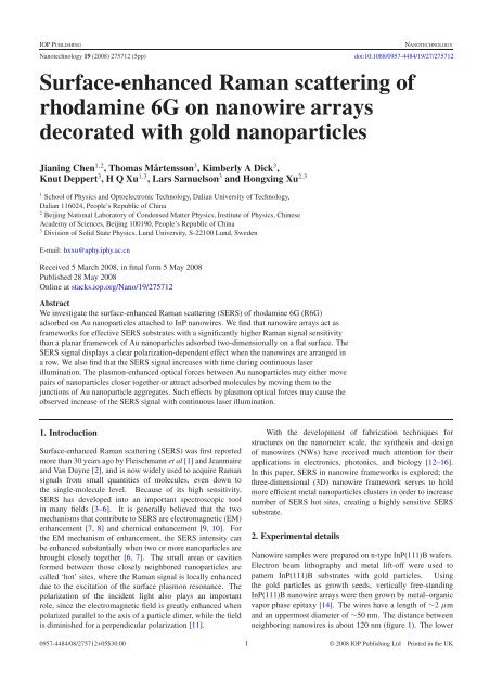
Figure 1. A45 ◦ tilted scanning electron microscopy image <strong>of</strong> an InP<br />
nanowire row, grown on an InP(111)B wafer from deposited aerosol<br />
phase Au nanoparticles. The Au nanoparticles, with a diameter <strong>of</strong><br />
∼50 nm (the white dots), are seen spread over the sample.<br />
limit on wire pitch was mainly determined by the resolution <strong>of</strong><br />
the electron beam lithography process. The nanowires were<br />
then decorated with aerosol phase gold nanoparticles [17].<br />
These size-selected nanoparticles <strong>of</strong> about 50 nm in diameter<br />
were generated by an evaporation/condensation method [18].<br />
After the decoration step, a droplet <strong>of</strong> 4 × 10 7 M R6G<br />
solution was placed on the nanowire sample, and dried before<br />
<strong>Raman</strong> measurements. The <strong>Raman</strong> spectra were collected in a<br />
back<strong>scattering</strong> geometry through a 100× objective HORIBA<br />
Jobin Yvon <strong>Raman</strong> spectrometer. The wavelength <strong>of</strong> laser<br />
excitation was 633 nm. The polarization <strong>of</strong> the incident light<br />
was set by rotating a half-wave plate mounted in the light path.<br />
<strong>Raman</strong> mapping was obtained by scanning the sample using<br />
step motors mounted on the microscope, with a step length <strong>of</strong><br />
300 nm.<br />
3. Results and discussions<br />
In figure 1, a row <strong>of</strong> NWs with deposited Au aerosols is<br />
shown. The Au nanoparticles are clearly seen as small<br />
white dots on both nanowires and the wafer surface. The<br />
free-standing nanowires are well separated. Figure 2 shows<br />
scanning electron microscopy (SEM) images <strong>of</strong> a nanowire<br />
row and a nanowire array after a droplet <strong>of</strong> R6G solution was<br />
applied on the substrate surface and dried; some nanowires<br />
are tilted and bound together because <strong>of</strong> the capillary force<br />
<strong>of</strong> the R6G solution as it dries. The capillary force changed<br />
the configuration <strong>of</strong> the nanowire row and array from separate<br />
pillars to a ‘shrub’. In this configuration, Au nanoparticles on<br />
the nanowires may come very close, forming SERS hot sites.<br />
The <strong>Raman</strong> mapping shows that hot sites do indeed exist in<br />
such nano-shrubs. Normally, large SERS takes place in the<br />
interstices between metal nanoparticles with distances <strong>of</strong> less<br />
than 5 nm. From previous studies, it was reported that the<br />
intensity is greatly <strong>enhanced</strong> when nanoparticles are placed<br />
Figure 2. SEM images <strong>of</strong> a nanowire row (left) and a nanowire array<br />
(right) decorated with aerosol phase Au nanoparticles after a droplet<br />
<strong>of</strong> R6G solution was applied and then dried. The wires are bent<br />
because <strong>of</strong> the capillary force <strong>of</strong> the R6G droplet as it dries.<br />
closely together, and the intensity can be built up by more<br />
than 11 orders <strong>of</strong> magnitude under certain conditions [7]. In<br />
principle, the quasi-one-dimensional template property <strong>of</strong> the<br />
nanowire allows efficient clustering <strong>of</strong> the Au nanoparticles<br />
favorable to SERS, if the incident polarization is parallel to<br />
the axis <strong>of</strong> the nanowire. In the back<strong>scattering</strong> experimental<br />
configuration used here, the focused light beam from the<br />
side <strong>of</strong> the objective lens has the component <strong>of</strong> the incident<br />
polarization parallel to the standing nanowire on the substrate,<br />
which benefits the SERS. But, the overall polarization effect<br />
<strong>of</strong> the incident light is perpendicular to the axis <strong>of</strong> a single<br />
standing nanowire in a polarization unfavorable configuration.<br />
However, the NW array serves as a 3D framework to carry<br />
more Au nanoparticles to create more ‘hot sites’ by those<br />
particles either between neighboring nanowires or along the<br />
nanowires than a flat surface, in order to enhance the SERS<br />
activity compared to a two-dimensional (2D) system.<br />
Figure 3 shows a typical <strong>Raman</strong> mapping image <strong>of</strong> a<br />
nanowire row. The bright spots are believed to be the hot sites<br />
formed by nanoparticles. Almost no detectable R6G <strong>Raman</strong><br />
signal can be collected from the surface <strong>of</strong> the wafer, although<br />
there are many Au nanoparticles present. The reason could<br />
be that the deposited Au nanoparticles on the wafer are well<br />
separated, and seldom aggregate [19] to create hot sites for<br />
strong SERS enhancement. The <strong>enhanced</strong> electromagnetic<br />
field around a single Au nanoparticle is too weak to enhance<br />
the <strong>Raman</strong> signal <strong>of</strong> the adsorbed molecules to a detectable<br />
level. The detected <strong>Raman</strong> signal is only acquired from the<br />
area where the nanowires exist, which provides evidence that<br />
3D NW structures serve as nanoparticle holders that have more<br />
nanoparticle aggregations than a 2D system. Such a 3D system<br />
could <strong>of</strong>fer stronger couplings between metal nanoparticles and<br />
form a better SERS substrate than a 2D system. Both coupling<br />
the excitation frequency to the particle plasmon resonance and<br />
alignment <strong>of</strong> the particles are essential to gain higher SERS<br />
enhancement <strong>of</strong> the nanoparticle clusters. On increasing the<br />
quasi-linear alignment <strong>of</strong> the Au particles along the nanowire,<br />
the coupling between the nanoparticles may shift the Au<br />
particle plasmon resonance from typically 550 nm (50 nm Au<br />
2
Nanotechnology 19 (2008) 275712<br />
Figure 3. <strong>Raman</strong> mapping image <strong>of</strong> a nanowire row (inset) and<br />
typical <strong>Raman</strong> spectrum <strong>of</strong> a bright spot (green cross site) in the<br />
<strong>Raman</strong> mapping image The accumulation time for each <strong>Raman</strong><br />
spectrum is 10 s, and the <strong>Raman</strong> mapping image is taken by scanning<br />
with the scanning step <strong>of</strong> 300 nm and an integration time <strong>of</strong> each spot<br />
10 s. The total time for each <strong>Raman</strong> mapping image is about 50 min.<br />
Considering the size <strong>of</strong> the laser spot to be about 2 μm, each spot<br />
actually experiences the laser illumination during the scanning about<br />
(2000/300) 2 × 10 ≈ 440 s.<br />
particles) to a position closer to 633 nm (laser used in the<br />
experiment), which can greatly increase the SERS efficiency.<br />
From previous study, it is known that the polarization<br />
<strong>of</strong> incident light can strongly influence SERS [11, 20–22].<br />
Different polarizations <strong>of</strong> the incident laser were used<br />
in the <strong>Raman</strong> mapping. A series <strong>of</strong> <strong>Raman</strong> mappings<br />
with different polarizations was obtained, as shown in<br />
figure 4. Six mapping images are shown with polarization <strong>of</strong><br />
0 ◦ , 30 ◦ , 60 ◦ , 90 ◦ , 120 ◦ , 150 ◦ in sequence, where 0 ◦ represents<br />
the polarization parallel to the nanowire row. From 0 ◦ to<br />
60 ◦ , the averaged <strong>Raman</strong> mapping intensity decreases; it<br />
JChenet al<br />
then starts to increase. It is clear that the averaged <strong>Raman</strong><br />
intensity is weakest when the polarization <strong>of</strong> the incident<br />
light is perpendicular to the nanowire row, although individual<br />
bright spots are still observed. This is not surprising since the<br />
randomly deposited Au nanoparticles may form hot aggregates<br />
in any direction. The polarization perpendicular to the axis<br />
<strong>of</strong> the NW row may in some cases be parallel to the axis<br />
<strong>of</strong> individual hot dimers, producing a strong SERS signal.<br />
However, the averaged <strong>Raman</strong> intensity is always higher when<br />
the incident polarization is nearly parallel to the nanowire<br />
row. This indicates that more hot sites are formed along the<br />
axis <strong>of</strong> the NW row when the NWs are bent together by the<br />
capillary force, as shown in figure 2. The photonic effect by<br />
far-separated nanoparticles along the nanowire row may also<br />
enhance the local field, and result in an increase <strong>of</strong> SERS<br />
signals in the parallel polarization [23, 24].<br />
It is interesting that, for every series <strong>of</strong> <strong>Raman</strong> mappings,<br />
the averaged intensity <strong>of</strong> each <strong>Raman</strong> mapping increases<br />
with the number <strong>of</strong> the series, although the polarization<br />
effect may initially decrease the <strong>Raman</strong> signals, as shown in<br />
figure 4. Since only the incident polarization is changed for<br />
the different <strong>Raman</strong> mapping in the series, while the laser<br />
illumination is always on, the total illumination time for each<br />
<strong>Raman</strong> mapping is proportional to the corresponding number<br />
in the series. In figure 4, for example, the last <strong>Raman</strong><br />
mapping has five times more laser illumination time than<br />
the first since it is also illuminated when the polarizations<br />
are changed in the previous five <strong>Raman</strong> mappings. This<br />
trend <strong>of</strong> increased SERS signals over time may be caused by<br />
the formation <strong>of</strong> additional aggregates due to the plasmonassisted<br />
<strong>enhanced</strong> optical force under the continuous laser<br />
illumination [25]. At the same time the adsorbed molecules<br />
may be also trapped in the junctions <strong>of</strong> nano-aggregates by<br />
the gradient optical forces owning to the huge <strong>enhanced</strong><br />
local field in the cavities between nanoparticles [26]. Since<br />
Figure 4. (a) <strong>Raman</strong> mapping images <strong>of</strong> a nanowire row at different polarizations <strong>of</strong> the laser excitation with the corresponding SEM image<br />
given at the bottom. (b) The corresponding averaged <strong>Raman</strong> intensities. Each <strong>Raman</strong> mapping image is obtained by scanning with the time <strong>of</strong><br />
about 50 min.<br />
3
Nanotechnology 19 (2008) 275712<br />
the interaction distance <strong>of</strong> the plasmon-assisted optical force<br />
between metal nanoparticles can be hundreds <strong>of</strong> nanometers,<br />
much larger than the interparticle distance in our experiments,<br />
it is possible to move nanoparticles close. Hence the optical<br />
force on nanoparticles may play an important role in creating<br />
hot aggregates with increased illumination time. The longer<br />
the time the sample is illuminated, the closer the distance is<br />
between the occasionally formed nano-aggregates. With this<br />
insight, the intensity increase with the serial number should be<br />
caused by a combination <strong>of</strong> the optical forces and the effect <strong>of</strong><br />
the polarization.<br />
The SERS intensity can be written as I (t,θ) = C(t)I (θ),<br />
where C(t) is the effective coefficient due to the influence<br />
<strong>of</strong> the optical force, and I (θ) = K cos 2 (θ) + M (K and<br />
M are coefficients) is the assumed polarization-dependent<br />
<strong>Raman</strong> intensity only if the influence <strong>of</strong> the optical force<br />
is ignored. It is generally agreed that the electromagnetic<br />
enhancement <strong>of</strong> SERS has two components. The first part is<br />
the local electromagnetic (EM) field intensity enhancement,<br />
which is | E loc<br />
E 0<br />
| 2 , where E loc is the local electric field and<br />
E 0 is the incident electric field, while the second part is the<br />
<strong>Raman</strong> emission enhancement driven by the antenna effect<br />
<strong>of</strong> metal nanostructures, which is again similar to | E loc<br />
E 0<br />
| 2 .<br />
That is why we get roughly | E loc<br />
E 0<br />
| 4 for the total SERS<br />
enhancement [3, 4]. However, this rough estimation is mainly<br />
valid to estimate the maximum EM enhancement, but may<br />
not be valid for the weaker EM enhancement, e.g. the EM<br />
enhancement for the unfavorable incident polarization. For<br />
the simplest clustering <strong>of</strong> close-packed metal nanoparticles,<br />
i.e. two particles, the first part <strong>of</strong> the EM enhancement, the<br />
local intensity enhancement, is | E max cos(θ)<br />
E 0<br />
| 2 ,whereE max is the<br />
maximum electric field in the cavity between two nanoparticles<br />
when the incident polarization is parallel to the axis <strong>of</strong> the two<br />
nanoparticles. This part <strong>of</strong> the EM enhancement has cos 2 (θ)<br />
dependence on the incident polarization. Since the induced<br />
electric field in the cavity between two nanoparticles (this<br />
part dominates the total SERS enhancement) always aligns<br />
to the axis <strong>of</strong> the two particles, regardless <strong>of</strong> the incident<br />
polarization, the molecule located in the cavity will have the<br />
same <strong>Raman</strong> emission behavior, which is determined by the<br />
antenna effect <strong>of</strong> metal nanostructures, but not by the incident<br />
polarization. The second part <strong>of</strong> SERS enhancement, i.e. the<br />
<strong>Raman</strong> emission enhancement, remains as | E max<br />
E 0<br />
| 2 , without<br />
polarization dependence. So the total EM enhancement should<br />
be | E max<br />
E 0<br />
| 4 cos 2 (θ), which still has cos 2 (θ) dependence on<br />
the incident polarization. We demonstrated recently that<br />
more complex clustering <strong>of</strong> nanoparticles also has the same<br />
cos 2 (θ) effect. Recent observation <strong>of</strong> the depolarization<br />
ratio cos(2θ) <strong>of</strong> the <strong>Raman</strong> scattered light indicates a similar<br />
content [20, 21]. Since the fluctuations <strong>of</strong> SERS normally<br />
took place, and the cos 2 (θ) and cos 4 (θ) dependences are quite<br />
close, it might be hard to resolve the cos 2 (θ) and cos 4 (θ)<br />
dependences clearly by experimental observation alone [11].<br />
In figure 4, the estimated C(t) and I (θ) are shown together<br />
with the experimental data. The increase <strong>of</strong> C(t) with the<br />
time accumulation <strong>of</strong> laser illumination (t is proportional<br />
to the number <strong>of</strong> the series N) indicates that the plasmonassisted<br />
optical forces can move the nanoparticles closer,<br />
JChenet al<br />
since the enhancement <strong>of</strong> SERS is roughly determined by<br />
the interparticle distance d as (1/d) 4 [27]. Considering that<br />
the Au nanoparticles are distributed three-dimensionally in<br />
the arrays/lines <strong>of</strong> the nanowires with different interparticle<br />
distances, the averaged effect <strong>of</strong> the optical force could be<br />
C(t) ∝ (1/d) β ,whereβ 4andd is the effective interparticle<br />
distance, which decreases with illumination time, 1/d ∝ t ∝<br />
(N − 1). The fitting in figure 4 (the blue line) C(t) =<br />
1 + 0.003 × (N − 1) 3 should indicate that the plasmon-assisted<br />
optical force plays an important role in our experiment.<br />
4. Summary<br />
In this paper nanowire structures serving as a framework to<br />
hold gold nanoparticles were used for the study <strong>of</strong> surface<strong>enhanced</strong><br />
<strong>Raman</strong> <strong>scattering</strong>. In such 3D structures, Au<br />
nanoparticles can come close enough to each other to create<br />
hot sites for huge enhancement <strong>of</strong> the SERS signal. From<br />
the <strong>Raman</strong> mapping, it is clear that strong <strong>Raman</strong> signals<br />
are acquired from the nanowire regions, but not for Au<br />
nanoparticles adsorbed on the surface <strong>of</strong> the wafer. The<br />
polarization dependence <strong>of</strong> SERS on rows <strong>of</strong> nanowires was<br />
also investigated. The <strong>Raman</strong> signal intensity is strong when<br />
the incident polarization is parallel to the nanowire row and<br />
weak for the perpendicular polarization. The facts that the<br />
weakest mapping intensity is not at 90 ◦ polarization and that<br />
the intensity <strong>of</strong> the measurement <strong>of</strong> <strong>Raman</strong> mapping after long<br />
laser illumination is much higher indicate that the plasmonassisted<br />
optical forces may play an important role. The optical<br />
forces can either drive a molecule to move to the junction <strong>of</strong><br />
the aggregates <strong>of</strong> Au nanoparticles or pull Au nanoparticles<br />
adsorbed on a nanowire closer together to create more ‘hot’<br />
sites. Both effects can cause the observed increase <strong>of</strong> SERS<br />
enhancement with continuous laser illumination.<br />
Acknowledgments<br />
We acknowledge the Nanometer Structure Consortium at Lund<br />
University, the Swedish Research Council (VR), the Swedish<br />
Foundation for Strategic Research (SSF), Knut and Alice<br />
Wallenberg Foundation, Ministry <strong>of</strong> Science and Technology<br />
(MOST) <strong>of</strong> China (Grant No. 2006DFB02020), and the<br />
‘Bairen’ project <strong>of</strong> the Chinese Academy <strong>of</strong> Sciences for their<br />
support and funding.<br />
References<br />
[1] Fleischmann M, Hendra P and McQuillan A 1974 Chem. Phys.<br />
Lett. 26 163<br />
[2] Jeanmaire D L and Van Duyne R 1977 J. Electroanal. Chem.<br />
84 1<br />
[3] Kneipp K, Kneipp H, Itzkan I, Dasari R and Feld M S 1999<br />
Chem. Rev. 99 2957<br />
[4] Moskovits M, Tay L L, Yang J and Haslett T 2002 Top. Appl.<br />
Phys. 82 215<br />
[5] Otto A 1984 Light Scattering in Solid IV ed M Cardona and<br />
G Guntherodt (Berlin: Springer) p 289<br />
[6] Xu H X, Bjerneld E J, Käll M and Börjesson L 1999 Phys. Rev.<br />
Lett. 83 4357<br />
4
Nanotechnology 19 (2008) 275712<br />
[7] Xu H X, Aizpurua J, Käll M and Apell P 2000 Phys. Rev. E<br />
62 4318<br />
[8] Moskovits M 1985 Rev. Mod. Phys. 57 783<br />
[9] Moskovits M 2005 J. <strong>Raman</strong> Spectrosc. 36 485<br />
[10] Campion A and Kambhampati P 1998 Chem. Soc. Rev.<br />
27 241<br />
[11] Xu H X and Käll M 2003 ChemPhysChem 4 1001<br />
[12] Cui Y, Wei Q Q, Park H K and Leiber C M 2001 Science<br />
293 1289<br />
[13] Drachev V P, Thoreson M D, Khaliullin E N, Davsiion V J and<br />
Shalaev V M 2004 J. Phys. Chem. B 108 18046<br />
[14] Mårtensson T, Borgström M, Seifert W, Ohlsson B J and<br />
Samuelson L 2003 Nanotechnology 14 1255<br />
[15] Samuelson L 2003 Mater. Today 6 22<br />
[16] Thelander C et al 2006 Mater. Today 9 28<br />
[17] Bayer K, Dick K A, Krinke T J and Deppert K 2007<br />
J. Nanopart. Res. 9 1211<br />
JChenet al<br />
[18] Magnusson M H, Deppert K, Malm J-O, Bovin J-O and<br />
Samuelson L 1999 Nanostruct. Mater. 12 45<br />
[19] Krinke T J, Deppert K, Magnusson M H, Schmidt F and<br />
Fissan H 2002 J. Aerosol Sci. 33 1341<br />
[20] Etchegoin P G, Galloway C and Le Ru E C 2006 Phys. Chem.<br />
Chem. Phys. 8 2624<br />
[21] Jiang J, Bosnick K, Maillard M and Brus L 2003 J. Phys.<br />
Chem. B 107 9964<br />
[22] Tong L M, Li Z P, Zhu T, Xu H X and Liu Z F 2008 J. Phys.<br />
Chem. C 112 7119<br />
[23] Zhao K, Xu H X, Gu B H and Zhang Z Y 2006 J. Chem. Phys.<br />
125 081102<br />
[24] Zou S L and Schatz G C 2005 Chem. Phys. Lett. 403 62<br />
[25] Svedbery F, Li Z P, Xu H X and Käll M 2006 Nano Lett.<br />
6 2639<br />
[26] Xu H X and Käll M 2002 Phys.Rev.Lett.89 246802<br />
[27] Xu H X, Wang X H, Persson M P, Xu H Q, Käll M and<br />
Johansson P 2004 Phys. Rev. Lett. 93 243002<br />
5


