A robust feedforward compensation scheme for multistage ...
A robust feedforward compensation scheme for multistage ...
A robust feedforward compensation scheme for multistage ...

Create successful ePaper yourself
Turn your PDF publications into a flip-book with our unique Google optimized e-Paper software.
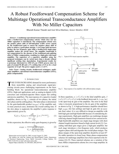
IEEE JOURNAL OF SOLID-STATE CIRCUITS, VOL. 38, NO. 2, FEBRUARY 2003 237<br />
A Robust Feed<strong>for</strong>ward Compensation Scheme <strong>for</strong><br />
Multistage Operational Transconductance Amplifiers<br />
With No Miller Capacitors<br />
Bharath Kumar Thandri and José Silva-Martínez, Senior Member, IEEE<br />
Abstract—A <strong>multistage</strong> operational transconductance amplifier<br />
with a <strong>feed<strong>for</strong>ward</strong> <strong>compensation</strong> <strong>scheme</strong> which does not use<br />
Miller capacitors is introduced. The <strong>compensation</strong> <strong>scheme</strong> uses<br />
the positive phase shift of left-half-plane (LHP) zeroes caused<br />
by the <strong>feed<strong>for</strong>ward</strong> path to cancel the negative phase shift of<br />
poles to achieve a good phase margin. A two-stage path increases<br />
further the low frequency gain while a <strong>feed<strong>for</strong>ward</strong> single-stage<br />
amplifier makes the circuit faster. The amplifier bandwidth is<br />
not compromised by the absence of the traditional pole-splitting<br />
effect of Miller <strong>compensation</strong>, resulting in a high-gain wide-band<br />
amplifier. The capacitors of a capacitive amplifier using the<br />
proposed techniques can be varied more than a decade without<br />
significant settling time degradation. Experimental results <strong>for</strong><br />
a prototype fabricated in AMI 0.5- m CMOS process show dc<br />
gain of around 90 dB and a 1% settling time of 15 ns <strong>for</strong> a load<br />
capacitor of 12 pF. The power supply used is 1.25 V.<br />
Index Terms—Analog circuits, <strong>feed<strong>for</strong>ward</strong> techniques, <strong>multistage</strong><br />
amplifiers, operational transconductance amplifiers (OTA),<br />
phase <strong>compensation</strong>.<br />
Fig. 1.<br />
Typical OTA-based capacitor amplifier.<br />
I. INTRODUCTION<br />
THE EVER-INCREASING demand <strong>for</strong> more per<strong>for</strong>mance<br />
from monolithic analog and mixed-mode signal-processing<br />
circuits poses challenging requirements on the basic<br />
building block: the operational transconductance amplifier<br />
(OTA). High-end applications such as analog-to-digital (A/D)<br />
converters and switched-capacitor filters require fast settling<br />
and precise amplifiers. The step response of a capacitive loaded<br />
amplifier, shown in Fig. 1, consists of two phases, the initial<br />
slew phase and the settling phase. The latter phase is determined<br />
by the gain-bandwidth product ( of the amplifier and,<br />
in many practical cases, dominates the overall settling time. If<br />
the slew phase is neglected, the amplifier’s pulse response is<br />
approximately given by<br />
In this expression, the effective unity-gain frequency is given by<br />
Manuscript received April 16, 2002; revised August 23, 2002.<br />
The authors are with the Analog and Mixed-Signal Center, Department<br />
of Electrical Engineering, Texas A&M University, College Station, TX<br />
77843-3128 USA (e-mail: jsilva@ee.tamu.edu).<br />
Digital Object Identifier 10.1109/JSSC.2002.807410<br />
(1)<br />
(2)<br />
Fig. 2.<br />
Step response of an amplifier with sufficient phase margin.<br />
In these equations,<br />
is the ideal amplifier gain,<br />
is the feedback factor and<br />
is the open-loop dc gain of the amplifier. The error in the final<br />
value is inversely proportional to the dc gain of the amplifier,<br />
as shown in Fig. 2. A high-per<strong>for</strong>mance amplifier should have<br />
high (<strong>for</strong> fast settling) and high dc gain (<strong>for</strong> an accurate<br />
final value). It is very difficult to design an amplifier with<br />
both high gain and high bandwidth because of contradicting design<br />
requirements. High-gain amplifiers use <strong>multistage</strong> designs<br />
with long channel length transistors biased at low current levels.<br />
High-bandwidth amplifiers use single-stage designs with short<br />
channel length transistors biased at high current levels [1]. Cascading<br />
individual gain stages gives a high-gain amplifier, but<br />
each stage introduces a low-frequency pole, which produces<br />
negative phase shift and degrades the overall phase margin. The<br />
phase margin of the open-loop amplifier should be at least 45<br />
<strong>for</strong> stable operation in closed loop. Many phase-<strong>compensation</strong><br />
<strong>scheme</strong>s <strong>for</strong> <strong>multistage</strong> amplifiers have been reported in the literature<br />
[2]–[7]. These reported <strong>scheme</strong>s are a variation of the<br />
basic Miller <strong>compensation</strong> <strong>scheme</strong> <strong>for</strong> a two-stage amplifier. In<br />
0018-9200/03$17.00 © 2003 IEEE
238 IEEE JOURNAL OF SOLID-STATE CIRCUITS, VOL. 38, NO. 2, FEBRUARY 2003<br />
Fig. 3.<br />
Block diagram of basic NCFF <strong>compensation</strong> <strong>scheme</strong> <strong>for</strong> two-stage amplifier.<br />
a Miller compensated amplifier, the dominant pole is pushed to<br />
lower frequencies due to the Miller effect (pole splitting), resulting<br />
in lower bandwidth structures. Also, a right-half-plane<br />
(RHP) zero is created which degrades the phase response. A<br />
nulling resistor is usually used to cancel the effect of the RHP<br />
zero. Other reported <strong>scheme</strong>s use the positive phase shift of a<br />
left-half-plane (LHP) zero created by a <strong>feed<strong>for</strong>ward</strong> path to improve<br />
the phase response [2], [4], but all of these still use Miller<br />
capacitors. Recently, active <strong>feed<strong>for</strong>ward</strong> techniques have been<br />
used <strong>for</strong> the design of <strong>multistage</strong> amplifiers. In [11], a theoretical<br />
analysis on the effects of <strong>feed<strong>for</strong>ward</strong> networks is presented, and<br />
in [12], the technique is used <strong>for</strong> the design of low-frequency instrumentation<br />
amplifiers.<br />
The <strong>compensation</strong> <strong>scheme</strong> used in this paper employs a <strong>feed<strong>for</strong>ward</strong><br />
path to create LHP zeros, but does not use any Miller<br />
capacitor. The dominant pole is not pushed to lower frequencies,<br />
resulting in a higher gain-bandwidth product with a fast<br />
step response. The proposed <strong>compensation</strong> <strong>scheme</strong> is described<br />
in Section II. The effects of pole–zero mismatch on the per<strong>for</strong>mance<br />
of the amplifier are discussed in Section III. It is shown<br />
that the proposed technique is <strong>robust</strong> even if the integrating and<br />
load capacitors are varied by more than a decade. Section IV<br />
describes the circuit implementation. The simulation and experimental<br />
results are discussed in Section V, and conclusions are<br />
drawn in Section VI.<br />
(a)<br />
(b)<br />
Fig. 4. Amplifier frequency response and pole–zero locations in open and<br />
closed loop. (a) Perfect pole–zero cancellation. (b) Pole–zero mismatch.<br />
II. NO-CAPACITOR FEEDFORWARD (NCFF) COMPENSATION<br />
SCHEME FOR MULTISTAGE AMPLIFIERS<br />
stages have a common pole at<br />
amplifier voltage gain is<br />
. The overall<br />
The proposed NCFF <strong>compensation</strong> <strong>scheme</strong> alleviates the<br />
drawbacks of Miller <strong>compensation</strong> <strong>scheme</strong>s. The block diagram<br />
of the NCFF <strong>scheme</strong> is shown in Fig. 3. The <strong>compensation</strong><br />
<strong>scheme</strong> uses the positive phase shift of LHP zeros, created by<br />
a <strong>feed<strong>for</strong>ward</strong> path, to compensate the negative phase shift due<br />
to the poles. The pole–zero pair is created at high frequencies<br />
to avoid slow settling components associated with pole–zero<br />
cancellation at low frequencies [8]. The main concept can be<br />
explained by assuming a single-pole response <strong>for</strong> the three<br />
blocks. , , and are the dc gains of the first, second,<br />
and <strong>feed<strong>for</strong>ward</strong> stages of the amplifier. The pole of the first<br />
stage is located at<br />
and the second and third<br />
The OTA transfer function has two poles and a LHP zero created<br />
by the <strong>feed<strong>for</strong>ward</strong> path. The dc gain is given by<br />
(3)
THANDRI AND SILVA-MARTÍNEZ: ROBUST FEEDFORWARD COMPENSATION SCHEME FOR MULTISTAGE OTAS WITH NO MILLER CAPACITORS 239<br />
Fig. 5.<br />
NCFF <strong>compensation</strong> <strong>scheme</strong> <strong>for</strong> n-stage amplifier.<br />
and the dominant pole is located at<br />
zero is<br />
. The location of the LHP<br />
Notice that the location of the LHP zero is approximately at<br />
times the gain-bandwidth product of the first stage, where<br />
. The second and <strong>feed<strong>for</strong>ward</strong> stages can be designed<br />
such that the negative phase shift due to is compensated by<br />
the positive phase shift of the LHP zero. When the frequency of<br />
exactly coincides with that of the LHP zero, the amplifier<br />
phase margin is 90 and the unity-gain frequency is given by<br />
. The open- and closed-loop transfer<br />
functions <strong>for</strong> perfect and imperfect pole–zero cancellation are<br />
shown in Fig. 4(a) and (b), respectively. The implications of<br />
pole–zero mismatch are discussed in Section III.<br />
This <strong>compensation</strong> <strong>scheme</strong> results in an amplifier with high<br />
gain and fast response. The bandwidth improvement is due to<br />
the fact that the poles are not split, as is the case in any amplifier<br />
with Miller <strong>compensation</strong>. There can be a substantial reduction<br />
in area and power, especially as compared to <strong>multistage</strong><br />
amplifiers, which use two or more capacitors <strong>for</strong> phase <strong>compensation</strong>.<br />
If the nondominant pole of the first stage is also considered,<br />
then the resulting transfer function has three poles and two<br />
LHP zeros. In general, the number of LHP zeros created by the<br />
<strong>feed<strong>for</strong>ward</strong> path is equal to the order of the first stage. The main<br />
restriction here is that the nondominant pole of the <strong>feed<strong>for</strong>ward</strong><br />
and second stage must be placed after the overall unity-gain<br />
bandwidth of the amplifier in order to minimize phase degradation.<br />
This <strong>compensation</strong> <strong>scheme</strong> can be extended <strong>for</strong> a generic<br />
-stage amplifier, as shown in Fig. 5.<br />
III. OPTIMIZATION OF CLOSED-LOOP RESPONSE<br />
The OTA is commonly used in closed-loop configuration with<br />
feedback capacitors as shown in Fig. 1. Imperfect pole–zero<br />
cancellation results in a pole–zero doublet that might affect the<br />
(4)<br />
per<strong>for</strong>mance of the amplifier. The transconductances of individual<br />
gain stages should be selected properly to alleviate this<br />
drawback, as shown in the following discussion.<br />
It has already been shown that a pole–zero doublet may<br />
degrade the settling time according to the pole–zero spacing<br />
and the zero’s frequency [8]. The closed-loop transfer function<br />
of a capacitive amplifier is affected by the feedback factor,<br />
as shown in (1) and (2). Usually, an amplifier with open-loop<br />
phase margin of around 60 –70 gives the fastest step response<br />
<strong>for</strong> the overall amplifier [9], [10]. However, the capacitive<br />
amplifier’s pulse response in the presence of a pole–zero<br />
doublet is more complex. Let us now consider the capacitive<br />
amplifier shown in Fig. 1 using the proposed OTA. By using<br />
typical circuit analysis techniques, it can be shown that the<br />
overall closed-loop transfer function is<br />
The zero and poles are given by<br />
where and are the effective<br />
OTA load capacitor and first-stage load capacitor (see Figs. 1<br />
and 3), respectively. The parameter<br />
is the feedback factor, and<br />
Notice that<br />
(5)<br />
(6)<br />
(7)<br />
(8)<br />
is the OTA output conductance.<br />
, and that real poles are obtained if<br />
. In (5), it is assumed<br />
that the frequency of the RHP zero due to gate–drain capacitors<br />
is placed at very high frequency, which is usually the case, and
240 IEEE JOURNAL OF SOLID-STATE CIRCUITS, VOL. 38, NO. 2, FEBRUARY 2003<br />
its effects can be neglected. For the sake of simplicity, other<br />
parasitic poles are not considered. If , the closed-loop<br />
amplifier pulse response can be obtained from (5) as<br />
(9)<br />
Low-frequency pole–zero pair degrades the settling-time per<strong>for</strong>mance<br />
and the slow-settling components can be avoided if<br />
the cancellation occurs at high frequencies. If and are not<br />
close to each other, dominates the speed of the system. For<br />
0.1% accuracy in the final value, a settling time of around s<br />
is required. If is around , then a settling time of around<br />
s is enough. Notice in (9) that the slowest component is<br />
associated with the closed-loop dominant pole , there<strong>for</strong>e it<br />
is important to match the frequency of the zero with this pole in<br />
order to minimize the settling time. If the amplifier is designed<br />
such that<br />
, the zero<br />
and poles are approximately located at the following frequencies:<br />
(10)<br />
Fig. 6.<br />
Single-ended amplifier with NCFF <strong>compensation</strong> <strong>scheme</strong>.<br />
TABLE I<br />
TRANSISTOR DIMENSIONS AND BIAS CURRENTS<br />
(11)<br />
(12)<br />
This condition guarantees that and are close to each<br />
other, regardless of the absolute value of capacitors used. This<br />
condition is illustrated in Fig. 4(b). It is worth mentioning<br />
that reducing the parasitic capacitors at the output of the first<br />
stage increases the frequency of both and and<br />
the pole–zero cancellation occurs at high frequencies. If the<br />
zero cancels the dominant pole, the speed of the amplifier<br />
is determined by the highest frequency pole— . Typical<br />
process parameter variations and different load conditions are<br />
such that the pole locations can change by a factor of two<br />
or three, but the mismatch between the dominant pole and<br />
the zero is much less than that, especially if the condition<br />
is satisfied. Another<br />
important point to be noted is that complex poles may appear<br />
<strong>for</strong> large load capacitors .<br />
IV. CIRCUIT REALIZATION<br />
The two-stage amplifier using the NCFF <strong>compensation</strong><br />
<strong>scheme</strong> has the following design considerations.<br />
1) The second and <strong>feed<strong>for</strong>ward</strong> stage should not have any<br />
nondominant pole be<strong>for</strong>e the overall .<br />
2) The pole–zero cancellation should occur at high frequencies<br />
<strong>for</strong> best settling-time per<strong>for</strong>mance.<br />
3) The overall amplifier’s dc gain should be high.<br />
These conditions can be met if the stages are chosen as<br />
follows. The first stage can be designed to have a high gain<br />
and small load capacitance. The second and <strong>feed<strong>for</strong>ward</strong> stages<br />
should be optimized <strong>for</strong> high bandwidth and medium gain per<strong>for</strong>mance.<br />
The schematic of the single-ended amplifier using<br />
the NCFF <strong>compensation</strong> <strong>scheme</strong> is shown in Fig. 6. The first<br />
stage (M1, M4, M5, M6) is a telescopic amplifier with high dc<br />
gain. The second (M2, M7) and <strong>feed<strong>for</strong>ward</strong> stages (M3, M7)<br />
are single-ended differential amplifiers. Equations (13)–(17)<br />
show the dc gain of the three stages, internal capacitor (load<br />
capacitor of first stage), and output conductance.<br />
(13)<br />
(14)<br />
(15)<br />
(16)<br />
(17)<br />
The design strategy is to place the LHP zero and the closed-loop<br />
dominant pole, which are given by (10) and (11), at the same<br />
frequency. The bias currents and aspect ratios of the second<br />
and <strong>feed<strong>for</strong>ward</strong> stage are adjusted such that<br />
. The transistor dimensions and bias currents are given<br />
in Table I. The amplifier was designed in AMI 0.5- m technology<br />
with a power supply of 1.25 V. Power-supply voltages<br />
of 0–2.5 V can also be used if the proper common-mode
THANDRI AND SILVA-MARTÍNEZ: ROBUST FEEDFORWARD COMPENSATION SCHEME FOR MULTISTAGE OTAS WITH NO MILLER CAPACITORS 241<br />
(a)<br />
Fig. 8.<br />
OTA pulse response in noninverting unity-gain (buffer) configuration.<br />
(b)<br />
Fig. 7. Open-loop ac response of the OTA. (a) Magnitude response. (b) Phase<br />
response.<br />
level (1.25 V) is generated. In the technology used, the typical<br />
threshold voltage of an nMOS transistor is 700 mV and<br />
<strong>for</strong> a pMOS transistor is 900 mV. The first stage of the amplifier<br />
(telescopic cascode) was designed <strong>for</strong> maximum gain<br />
per<strong>for</strong>mance and relatively small time constant (<br />
pF/700 AV ns). The swing of the first stage need<br />
not be high (it is typically in the order of a few millivolts) as it is<br />
amplified further by the gain of the second stage. The dc bias of<br />
transistor M1 is at ground and the dc bias <strong>for</strong> M4 and M5 are set<br />
by a bias circuit. The transconductance of the second and <strong>feed<strong>for</strong>ward</strong><br />
stage is increased as much as possible to push the poles<br />
to high frequencies: mA/V and mA/V.<br />
Since the values of the first pole and the LHP zero depend on<br />
parasitic capacitances and the feedback factor, exact cancellation<br />
may not be possible; however, the effect of the pole–zero<br />
mismatch is small because the partial cancellation occurs at high<br />
frequencies.<br />
This structure is well suited <strong>for</strong> fully differential implementation,<br />
where the reduced number of parasitic poles (due to the<br />
absence of differential to single-ended conversions) makes the<br />
structure faster. In this case, additional common-mode feedback<br />
circuits have to be added <strong>for</strong> both the first and second stage to<br />
control the common-mode voltages.<br />
V. EXPERIMENTAL AND SIMULATION RESULTS<br />
The simulated open-loop ac magnitude and phase response<br />
of the single-ended OTA is shown in Fig. 7(a) and (b), respec-<br />
Fig. 9. Pulse response post-layout simulation—parametric sweep of feedback<br />
and load capacitors.<br />
Fig. 10.<br />
Microphotograph of the OTA.<br />
tively. The load capacitor used in the simulations was 8 pF<br />
and the design was optimized <strong>for</strong> this loading. The OTA dc<br />
gain, unity-gain frequency, and phase margin are around 94 dB,<br />
300 MHz, and 74 , respectively. The OTA pulse response <strong>for</strong><br />
a noninverting unity-gain configuration (buffer configuration)<br />
loaded by a capacitor of 8 pF is shown in Fig. 8. An input step<br />
of 400 mV and 100-ps rise time was used <strong>for</strong> the simulations,<br />
and 1% settling time is less than 7 ns. Parametric sweep simulations<br />
<strong>for</strong> the capacitive amplifier with<br />
(see
242 IEEE JOURNAL OF SOLID-STATE CIRCUITS, VOL. 38, NO. 2, FEBRUARY 2003<br />
Fig. 13.<br />
Measured pulse response <strong>for</strong> large input signal.<br />
Fig. 11. Experimental results <strong>for</strong> the single-ended amplifier. Input step (falling<br />
edge) signal and amplifier response.<br />
TABLE II<br />
POST-LAYOUT SIMULATION AND EXPERIMENTAL RESULTS<br />
WITH LOAD CAPACITOR OF 12 pF<br />
*Due to noise limitations, 0.1% settling time was difficult to measure properly.<br />
Fig. 12. Post-layout simulation results <strong>for</strong> the capacitive amplifier. Pulse<br />
response with a real input signal, including all parasitic capacitors. 1% settling<br />
time is around 14 ns.<br />
Fig. 1 <strong>for</strong> the identification of the capacitors) are shown in Fig. 9.<br />
The values used <strong>for</strong> the capacitors are 0.25, 0.5, 1, 3, 7, and<br />
10 pF. The amplifier’s output represents the typical exponential<br />
behavior of an underdamped system and the phase margin is always<br />
greater than 45 . The 1% settling time is 2.4 and 8 ns <strong>for</strong><br />
capacitors of 0.25 and 10 pF, respectively, when the input step<br />
had a fall time of 100 ps. The feedback and loop gain factors<br />
are reduced if the parasitic capacitors are comparable with the<br />
main capacitors, and the parasitic poles and the RHP zero cannot<br />
be neglected because they are comparable with . These poles<br />
and zeros introduce negative excess phase, reducing the phase<br />
margin. A small overshoot appears in the pulse response of the<br />
amplifier <strong>for</strong> small capacitors of less than 3 pF, which can be observed<br />
in Fig. 9. Also, the effects of the drain–gate capacitor of<br />
transistor M3 are evident in these simulations. increases<br />
the effective feedback capacitor and this effect can be avoided<br />
if cascode amplifier is used in the <strong>feed<strong>for</strong>ward</strong> stage.<br />
The single-ended amplifier was fabricated in the AMI<br />
0.5- m technology through the MOSIS Educational program.<br />
The chip microphotograph is shown in Fig. 10. The active area<br />
<strong>for</strong> the amplifier is around 0.16 mm . An inverting capacitive<br />
amplifier, similar to the one shown in Fig. 1, was used <strong>for</strong><br />
measuring the OTA pulse response. For the test setup, external<br />
capacitors of 5 pF were employed and the load capacitance<br />
was 12 pF (estimated capacitance of measurement equipment<br />
probe capacitance and package bond-pad capacitance). The<br />
pulse response of the fabricated OTA was measured and is<br />
shown in Fig. 11. The 1% settling time <strong>for</strong> an input step of<br />
0.7 V was 15 ns—around 8 ns corresponds to slew-rate phase<br />
and 7 ns are associated with the settling phase limited by the<br />
effective gain–bandwidth product. For these results, the input<br />
edge had a fall time of around 3 ns. It was difficult to obtain<br />
a better step input due to the printed circuit board (PCB),<br />
bond-pad parasitics (DIP-40 package was used), and equipment<br />
loading effects. The output step response has no ringing, which<br />
shows a good phase margin. Post-layout simulation result <strong>for</strong><br />
the amplifier is shown in Fig. 12, with a 3-ns fall-time input<br />
step. The feedback and load capacitors are similar to the ones<br />
indicated in the measurement setup. The 1% settling time is<br />
around 14 ns, which is in con<strong>for</strong>mance with the measured<br />
results. The 0.1% settling time is around 20 ns. Monte Carlo<br />
simulations including 1% transistor mismatches have shown<br />
almost no effect on the speed of the amplifier.<br />
The ac voltage at the noninverting terminal was very small,<br />
even below the noise level. From measurements, the dc gain was<br />
estimated to be around 90 dB. The OTA pulse response <strong>for</strong> large<br />
input signals (up to 1 V) is shown in Fig. 13 and most of the<br />
settling time is due to slew-rate limitation. The input-referred<br />
noise density is around 10.3 nV/Hz . and gain
THANDRI AND SILVA-MARTÍNEZ: ROBUST FEEDFORWARD COMPENSATION SCHEME FOR MULTISTAGE OTAS WITH NO MILLER CAPACITORS 243<br />
transfer functions are around 6 and 10 dB at low frequencies,<br />
respectively. Post-layout simulation and experimental results<br />
<strong>for</strong> the single-ended amplifier using integrating and feedback<br />
capacitors of 5 pF are compared in Table II.<br />
CONCLUSION<br />
A <strong>compensation</strong> <strong>scheme</strong> <strong>for</strong> <strong>multistage</strong> amplifiers with no<br />
Miller capacitors was proposed. This <strong>scheme</strong> uses positive<br />
phase shift of LHP zeros created by the <strong>feed<strong>for</strong>ward</strong> path<br />
to cancel the negative phase shift of the poles (closed-loop<br />
dominant pole). A single-ended amplifier using the proposed<br />
NCFF <strong>compensation</strong> <strong>scheme</strong> was designed and fabricated in<br />
AMI 0.5- m technology. The amplifier combines high gain,<br />
high gain bandwidth, and good phase margin. Pulse response<br />
shows that the phase margin is better than 45 <strong>for</strong> capacitors in<br />
the range of 0.25–10 pF. The effect of pole–zero mismatch on<br />
the amplifier per<strong>for</strong>mance was studied and it was shown that<br />
the pole–zero cancellation should occur at high frequencies<br />
<strong>for</strong> best settling-time per<strong>for</strong>mance. Experimental results of the<br />
OTA show fast settling time and good stability.<br />
[11] M. Schlarmann, E. Lee, and R. Geiger, “A new multipath amplifier design<br />
technique <strong>for</strong> enhancing gain and bandwidth,” in Proc. IEEE Int.<br />
Symp. Circuits and Systems, vol. II, June 1999, pp. 610–615.<br />
[12] A. Thomsen, “A five-stage chopper stabilized instrumentation amplifier<br />
using <strong>feed<strong>for</strong>ward</strong> <strong>compensation</strong>,” in Proc. Symp. VLSI Circuits, Honolulu,<br />
HI, June 1998, pp. 220–223.<br />
Bharath Kumar Thandri received the B.E. (Hons)<br />
degree in computer science from Birla Institute of<br />
Technology and Science, Pilani, India, in 1998 and<br />
the M.S. degree in electrical engineering from Texas<br />
A&M University, College Station, in 2001.<br />
From 1998 to 1999, he worked in the DSP group of<br />
Texas Instruments (India) Ltd., Bangalore, where he<br />
developed software simulators <strong>for</strong> TI’s C6X range of<br />
DSPs. He was an Intern in the Computer Peripherals<br />
and Control Products Group of Texas Instruments,<br />
Dallas, TX, in the fall of 2000. Since November 2001,<br />
he has been with Cypress Semiconductors, Austin, TX, where he is working<br />
on the design of optical communication transceiver ICs and mixed-signal CAD<br />
flow development. His main research interests are in the area of high-per<strong>for</strong>mance<br />
and high-frequency analog circuits <strong>for</strong> communication and signal-processing<br />
ICs.<br />
REFERENCES<br />
[1] K. Bult and G. J. G. M. Geelen, “A fast-settling CMOS OpAmp <strong>for</strong> SC<br />
circuits with 90-dB dc gain,” IEEE J. Solid-State Circuits, vol. 25, pp.<br />
1379–1384, Dec. 1990.<br />
[2] R. Eschauzier and J. H. Huijsing, Frequency Compensation Techniques<br />
<strong>for</strong> Low-Power Operational Amplifiers. Boston, MA: Kluwer, 1995.<br />
[3] K. N. Leung, P. K. T. Mok, W. H. Ki, and J. K. O. Sin, “Three-stage<br />
large capacitive load amplifier with damping-factor-control frequency<br />
<strong>compensation</strong>,” IEEE J. Solid-State Circuits, vol. 35, pp. 221–230, Feb.<br />
2000.<br />
[4] F. You, S. H. K. Embabi, and E. Sanchez-Sinencio, “A <strong>multistage</strong> amplifier<br />
topology with nested Gm–C <strong>compensation</strong> <strong>for</strong> low-voltage application,”<br />
IEEE J. Solid-State Circuits, vol. 32, pp. 2000–2011, Dec.<br />
1997.<br />
[5] R. Eschauzier, L. P. T. Kerklaan, and J. H. Huijsing, “A 100-Mhz 100-dB<br />
operational amplifier with multipath nested Miller <strong>compensation</strong> structure,”<br />
IEEE J. Solid-State Circuits, vol. 27, pp. 1709–1717, Dec. 1992.<br />
[6] R. Eschauzier, R. Hogervorst, and J. H. Huijsing, “A programmable<br />
1.5-V CMOS class-AB operational amplifier with hybrid nested Miller<br />
<strong>compensation</strong> <strong>for</strong> 120-dB gain and 6-MHz UGF,” IEEE J. Solid-State<br />
Circuits, vol. 29, pp. 1497–1504, Dec. 1994.<br />
[7] H. T. Ng, R. M. Ziazadeh, and D. J. Allstot, “A <strong>multistage</strong> amplifier<br />
technique with embedded frequency <strong>compensation</strong>,” IEEE J. Solid-State<br />
Circuits, vol. 34, pp. 339–347, Mar. 1999.<br />
[8] Y. B. Kamath, R. G. Meyer, and P. R. Gray, “Relationship between frequency<br />
response and settling time of operational amplifiers,” IEEE J.<br />
Solid-State Circuits, vol. 9, pp. 347–352, Dec. 1974.<br />
[9] H. C. Yan and D. J. Allstot, “Considerations <strong>for</strong> fast settling operational<br />
amplifiers,” IEEE Trans. Circuits Syst. II, vol. 37, pp. 326–334, Mar.<br />
1990.<br />
[10] U. Chilakapati and T. Fiez, “Settling time design considerations <strong>for</strong> SC<br />
integrators,” IEEE Trans. Circuits Syst. II, vol. 46, pp. 810–816, June<br />
1999.<br />
José Silva-Martínez (SM’98) was born in<br />
Tecamachalco, Puebla, México. He received the<br />
B.S. degree in electronics from the Universidad<br />
Autónoma de Puebla in 1979, the M.Sc. degree<br />
from the Instituto Nacional de Astrofísica Optica y<br />
Electrónica (INAOE), Puebla, in 1981, and the Ph.D.<br />
degree from the Katholieke Univesiteit Leuven,<br />
Leuven, Belgium, in 1992.<br />
From 1981 to 1983, he was with the Department<br />
of Electrical Engineering, INAOE, where he was<br />
involved with switched-capacitor circuit design.<br />
In 1983, he joined the Department of Electrical Engineering, Universidad<br />
Autónoma de Puebla, where he remained until 1993. He was a cofounder of<br />
the graduate program on opto-electronics in 1992. From 1985 to 1986, he was<br />
a Visiting Scholar in the Department of Electrical Engineering, Texas A&M<br />
University, College Station. In 1993, he rejoined the Department of Electrical<br />
Engineering, INAOE, and from May 1995 to December 1998, was the Head<br />
of the Electronics Department. He was a cofounder of the Ph.D. program on<br />
electronics in 1993. He is currently with the Analog and Mixed Signal Center,<br />
Department of Electrical Engineering, Texas A&M University, where he is<br />
an Associate Professor. He is the inaugural holder of the TI Professorship I<br />
in Analog Engineering, Texas A&M University. His current field of research<br />
is in the design and fabrication of integrated circuits <strong>for</strong> communication and<br />
biomedical application.<br />
Dr. Silva-Martínez has served as IEEE Circuits and Systems Vice President<br />
Region 9 (1997–1998), and as Associate Editor <strong>for</strong> IEEE TRANSACTIONS ON<br />
CIRCUITS AND SYSTEMS PART II from 1997 to 1998 and May 2002 until the<br />
present. He was the main organizer of the 1998 and 1999 International IEEE<br />
Circuits and Systems Tour in region 9, and Chairman of the International Workshop<br />
on Mixed-Mode IC Design and Applications (1997–1999). He was a corecipient<br />
of the 1990 European Solid-State Circuits Conference Best Paper Award.