Doping and characterization of graphene and graphene nanowalls
Doping and characterization of graphene and graphene nanowalls
Doping and characterization of graphene and graphene nanowalls

Create successful ePaper yourself
Turn your PDF publications into a flip-book with our unique Google optimized e-Paper software.
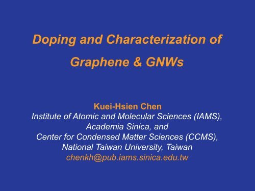
<strong>Doping</strong> <strong>and</strong> Characterization <strong>of</strong><br />
Graphene & GNWs<br />
Kuei-Hsien Chen<br />
Institute <strong>of</strong> Atomic <strong>and</strong> Molecular Sciences (IAMS),<br />
Academia Sinica, <strong>and</strong><br />
Center for Condensed Matter Sciences (CCMS),<br />
National Taiwan University, Taiwan<br />
chenkh@pub.iams.sinica.edu.tw
Outline<br />
Introduction<br />
N-doping <strong>of</strong> GNWs<br />
BN-codoping <strong>of</strong> <strong>graphene</strong><br />
In-situ doping<br />
XPS, UV-Vis analysis<br />
STEM analysis<br />
XES & XANES analysis<br />
Summary
Gap-opening in Graphene<br />
Science 2011, 313, 951<br />
Nature 2009, 458, 872<br />
Phys. Rev. Lett. 2006, 97, 216803<br />
J. Phys. Chem. C 2011, 115, 3250<br />
ACS Nano 2011, 5, 385<br />
ACS Nano 2010, 4, 7619<br />
J. Appl. Phys. 2010, 108, 073711
B-N Co-doping<br />
Ammonia Borane<br />
Evidence for hybridized h-BN <strong>and</strong> <strong>graphene</strong><br />
domain-like structure <strong>of</strong> h-BCN<br />
B<strong>and</strong> gap Calculation<br />
Pure h-BN<br />
5.69eV<br />
16% BN<br />
1.51eV<br />
3.85eV<br />
35% BN<br />
1.62eV<br />
4.48eV<br />
Pulickel M. Ajayan et al. Nature Materials, 9, 430 (2010)
Outline<br />
Introduction<br />
N-doping <strong>of</strong> GNWs<br />
BN-codoping <strong>of</strong> <strong>graphene</strong><br />
In-situ doping<br />
XPS, UV-Vis analysis<br />
STEM analysis<br />
XES & XANES analysis<br />
Summary
Growth <strong>of</strong> Graphene Nanowalls<br />
Microwave Plasma CVD reactor<br />
(MWCVD)<br />
SiH 4 / CH 4 /H2 plasma<br />
Source reactants: SiH 4 / CH 4 / H 2<br />
Gas ambient : H 2<br />
Microwave power :1000-2000 W<br />
Growth temperature : 900-1100 0 C<br />
<br />
3.5x3.5 cm 2<br />
Si<br />
Si<br />
Carbon 49, 4911 (2011)
Large-Scale Production<br />
Ultrathin Sheet-like Morphology<br />
3.5x3.5 cm 2<br />
Thickness : 4 -7 nm
Microstructures<br />
[101]<br />
0.23 nm<br />
100 nm<br />
[002]<br />
0.25 nm<br />
2 nm<br />
2009 Cross-Strait Workshop
Schematic <strong>of</strong> Hybrid GNWs Growth<br />
A<br />
C<br />
<br />
<br />
<br />
<br />
SiC <br />
<br />
<br />
<br />
<br />
<br />
Si<br />
B<br />
Si<br />
SiC<br />
D
Layer Number Control<br />
5 nm<br />
5 nm<br />
5 nm<br />
<br />
Carbon 49, 4911 (2011)
TEM Analysis<br />
SiC<br />
<br />
5nm
GNWs for Supercapacitors
Supercapacitors
GNWs on CC
Capacitor Performance<br />
<br />
<br />
<br />
<br />
<br />
<br />
<br />
<br />
<br />
<br />
<br />
<br />
<br />
<br />
<br />
<br />
<br />
<br />
<br />
<br />
<br />
<br />
<br />
Current Density(mA/cm 2 )<br />
8<br />
6<br />
4<br />
2<br />
0<br />
-2<br />
-4<br />
-6<br />
-8<br />
0.0 0.2 0.4 0.6 0.8 1.0<br />
Potential(V vs Ag/AgCl)<br />
CNWs/CC<br />
CC only
N-
Where does N sit in <strong>graphene</strong><br />
<br />
<br />
<br />
<br />
<br />
<br />
Li et al. JACS 131, 15939 (2009)<br />
Wang et al. ACS Nano 4, 1790 (2010)
Intensity (a.u.)<br />
<br />
<br />
Itensity (a.u.)<br />
<br />
<br />
294 291 288 285 282 279 276<br />
Binding Energy (eV)<br />
<br />
294 291 288 285 282 279 276<br />
Binding Energy (eV)<br />
<br />
Intensity (a.u.)<br />
<br />
Intensity (a.u.)<br />
405 400 395 390 385<br />
Binding Energy (eV)<br />
410 405 400 395 390<br />
Binding Energy (eV)
Intensity (a.u.)<br />
<br />
<br />
Itensity (a.u.)<br />
<br />
<br />
294 291 288 285 282 279 276<br />
Binding Energy (eV)<br />
<br />
294 291 288 285 282 279 276<br />
Binding Energy (eV)<br />
<br />
Intensity (a.u.)<br />
<br />
Intensity (a.u.)<br />
405 400 395 390 385<br />
Binding Energy (eV)<br />
410 405 400 395 390<br />
Binding Energy (eV)
Outline<br />
Introduction<br />
N-doping <strong>of</strong> GNWs<br />
BN-codoping <strong>of</strong> <strong>graphene</strong><br />
In-situ doping<br />
XPS, UV-Vis analysis<br />
STEM analysis<br />
XES & XANES analysis<br />
Summary
In-situ BN-doping<br />
Advantages:<br />
• In situ BN doping<br />
• Large-scaled growth<br />
• Easy control <strong>of</strong> BN concentration in <strong>graphene</strong>
XPS <strong>and</strong> TEM Analysis
Raman Analysis<br />
• Clear evidence <strong>of</strong> BN domains in high BN-doped<br />
(>27%) <strong>graphene</strong>.
FET Analysis<br />
• Semiconducting behavior is observed for 3% BN in<br />
<strong>graphene</strong>.
FE Characteristic
Optical Absorption
Summary<br />
N-doped GNWs/CC provides the<br />
material for EC applications such as<br />
supercapacitor.<br />
Evidence <strong>of</strong> gap-opening via BNcodoping<br />
<strong>of</strong> <strong>graphene</strong> is proposed.
Acknowledgement<br />
C.C. Kuo, C.K. Chang, Dr. S. Kataria, Dr. B.Y. Wang<br />
Pr<strong>of</strong>. S. Isota, Pr<strong>of</strong>. W.F. Pong, Pr<strong>of</strong>. Li-Chyong Chen<br />
Funding<br />
National Science Council <strong>and</strong> Academia Sinica, Taiwan<br />
AOARD, AFOSR