Create successful ePaper yourself
Turn your PDF publications into a flip-book with our unique Google optimized e-Paper software.
<strong>Ultra</strong> <strong>Flanger</strong><br />
Design by John Hollis<br />
The <strong>Ultra</strong> <strong>Flanger</strong>isJohn Hollis' design of avery flexible flanger based on<br />
the MN3007 bucket-brigade analog delay chip.<br />
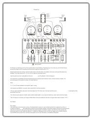
U1A is an input amplifierand mixer.The inputsignal comes in through C1<br />
and R2 where it meets theRegen feedback signal from oneside of the<br />
Odd/EvenRegen switch.R1 is apulldown resistortoprevent popping when<br />
switched.R3 biases U1A (and through itU3 and U1B)to Vbias1, about4.9V.<br />
U1Ahas aslight gain boost.<br />
The outputfrom U1Agoes to two places: through R5 to the inputto U2 for<br />
delay processingand to the output through R12 to be mixed with the delayed<br />
signalout of U2.The signal level at the inputto U2 is limited byD1and D2 -<br />
these are not fordeliberate distortion.The output ofU2 is available atpins 7<br />
and 8, and this is thenapplied to U1B, which low pass filters thedelayed<br />
signaltoremove thesampling noise caused by U2's analogsampling.The<br />
lowpass filtered signalis mixed withthe drysignal through R13, and goes to<br />
the output jack throughC5.The outputofU1Balso feedsthe Regen control to<br />
determinethe amountof feedback to bemixed with the input.<br />
U5A serves asaSchmitt triggerto determine the min andmax size ofthe<br />
LFO triangle wave. U5Bis an integrator that ramps up and down, controlled<br />
bythe output signalofU5A. Theamount of U5A's output that is applied to<br />
U5B's input is controlled by the Ratecontrol;this determines how fast the<br />
integratorramps.<br />
U5B's outpugoes to the Sweep control,which determines how large a<br />
triangle wave is fed to the highfrequency clock generator, U4. The triangle is<br />
further smoothed by R23/C9.<br />
U4generates abiphase output on pins 2and 3/4 at aspeed determined by<br />
the voltageon its pin 9.This outputis between 50kHz and1MHz. It is buffered<br />
bythe paralleled sections ofU3, andthis drives theclock inputs of U2.<br />
Count Value Designation(s)<br />
5 1N914 D1,D2,D3,D4,D5<br />
2 Red LED1,2<br />
2 DualOpamp U1,U5<br />
1 MN3007 U2<br />
1 CD4049 U3<br />
1 CD4046 U4<br />
1 100R R27<br />
1 470R R21<br />
1 2.7k(2K7) R24<br />
5 10K R12,R13,R15,R17,R5<br />
1 12K R16<br />
1 22K R22<br />
1 39k R24<br />
4 47K R11,R19,R7,R8<br />
1 68K R3<br />
7 100K R10,R14,R18,R2,R23,R6,R9<br />
Count Value Designation(s)<br />
1 150K R4<br />
1 470K R20<br />
1 3.3M (3M3) R26<br />
1 10M R1<br />
1 5Ktrimpot Tr3<br />
2 100Ktrimpot Tr1,Tr2<br />
1 22pF C10<br />
2 0.001uF(1nF) C3,4<br />
1 0.0047uF(4n7) C2<br />
1 0.1uF(100nF) cer C11<br />
2 0.1uF(100nF) C1,8<br />
2 1uFradialelectro C5,C9<br />
1 10uFrad electro C7<br />
1 100uFrad electro C6<br />
6 0.4" wirejumper J1,J2,J3,J4,J5,J6<br />
Revisions History<br />
10/26/01:Firstrelease.<br />
04/07/02:Corrected schematic and layoutper John Hollis Instructions.<br />
Previous Hollis schematic incorrectly connectedC9 and R24<br />
toVbias,not ground.<br />
IN<br />
From<br />
Stomp<br />
Sw<br />
C6<br />
C1<br />
1<br />
R1<br />
+9<br />
Odd/Even<br />
TR3*<br />
See Text!<br />
TR1<br />
TR2<br />
C2<br />
R4<br />
R6<br />
REGEN<br />
+9<br />
1<br />
appx 4.9V +9<br />
R2<br />
1<br />
2<br />
8<br />
C3 6 8<br />
- 1 R5 3<br />
-<br />
U2<br />
7<br />
-<br />
R3<br />
U1a<br />
R8<br />
U1b<br />
3<br />
7<br />
5<br />
+ +<br />
R13 +<br />
4<br />
C5<br />
R11<br />
R15<br />
+9 D1<br />
4 5 6 2<br />
appx 4.9V<br />
appx 4.9V<br />
D2<br />
1<br />
C4<br />
+9<br />
15 14<br />
R14<br />
R17 1<br />
12<br />
1 appx 3.8V<br />
11<br />
1<br />
+9<br />
appx 4.9V 2<br />
10<br />
LED1<br />
50kHz to 1MHz<br />
10<br />
U3<br />
LED2<br />
50kHz to 1MHz<br />
R27<br />
R16 C7<br />
2 3<br />
D3<br />
justunder 9V<br />
4 5<br />
R7<br />
R9<br />
R10<br />
R12<br />
OUT<br />
to<br />
Stomp<br />
SW<br />
+<br />
-<br />
R19<br />
R18<br />
U5a<br />
R20<br />
2 Flips from<br />
2<br />
over7V<br />
down to R21<br />
almost0V<br />
C8<br />
-<br />
U5b<br />
+<br />
R22<br />
Ramps up<br />
and down<br />
around 3.8V<br />
D4<br />
D5<br />
2 2<br />
appx 3.8V<br />
R23<br />
+<br />
C9<br />
-<br />
6<br />
8<br />
7<br />
R24<br />
9<br />
C11<br />
2 3 4 14 16<br />
U4<br />
5 8 11 12 6 7<br />
R25 R26 C10<br />
2<br />
Copyright 2001 R.G.Keen.All rights reserved. No permission forlocal copies ordisplayfrom web sites other than http://www.geofex.com.
<strong>Ultra</strong> <strong>Flanger</strong><br />
Design by John Hollis<br />
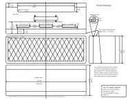
Making thecircuit board<br />
I've received som comments that the normal trace<br />
spacing Iuse gets eaten awayabit by printerand<br />
file conversion tolerances, making the pads and<br />
traces abitfatter. Because this is avery busy<br />
board, I've pre-compensatedfor that by making the<br />
majority of the tracesabit thinner.Most arelaid out<br />
as0.020" (20mils)wide.<br />
Tomake thecircuit board,print the pattern to<br />
tonerpaper.Press-N-Peel Blue is recommended,<br />
because the smaller traces will betrickier withother<br />
tonertransfertypes. Thepatternis thecorrectway<br />
'round fortonertransfer printing.<br />
Irecommend printing thepatterndirectly ontothe<br />
paper. Agood way todo this is to printthis sheet<br />
onto paper,then cut out arectangle of PNP Blue<br />
that is slightly larger than the toner section. Tape<br />
this to the previously printed paper sheet; tape<br />
along theleading edge of the tonersection. Now<br />
printthe sheetagain, manually feeding it into your<br />
printer.Resolution and accuracy will be best on an<br />
original print,not aprint thatis then copied.<br />
Follow the instructions for the toner sheet. Clean<br />
the copper board very,very well. Mostfailures are<br />
due to improper cleaning ofthe board. Iron the<br />
sheet onto yourcopperclad blank. If you look atthe<br />
shiny sideof the sheet at agrazingangle,youcan<br />
see the slight indentation where the toner on the<br />
bottom side is adhering to the copper.Do not iron<br />
somuch thatthe pattern spreads. If you foul it up,<br />
justclean the toneroff the copperwith acetone,<br />
then printand iron another. Do any necessary<br />
touch up withaSharpie marker or aRadio Shack<br />
etch resistpen -which Ithink is arelabeled<br />
Sharpie.<br />
Etchin your favoriteetchant. Ilike ferric chloride,<br />
even though it's messy and smells bad.<br />
Drillwith a0.030" drillbit.It helps to indent the<br />
centers of the pads abit withasharp pointe too like<br />
anice pick.<br />
Input<br />
DPDT<br />
Stomp<br />
Sw<br />
Odd/<br />
Even<br />
Regen<br />
100KLog<br />
Output<br />
Rate<br />
100KLog<br />
ToControlline,<br />
Millenium Bypass<br />
Battery<br />
Clip<br />
Sweep<br />
100KLog<br />
Manual<br />
100KLog<br />
The fifth pad from the leftisaground pad. Itcan<br />
beused to ground the outputjack,orjus left open<br />
asin the wiring diagram.<br />
Notes on the layout:<br />
I've addedacouple of things to the design.R27/C11 decouples the digital noise<br />
from U3 and U4 from the analog+9V.You mightbe able to sub in ajumperfor<br />
R27and leave C11 out if you like living dangerously. Trimmer TR3 is there for<br />
tweaking in the analog bias voltage.The pads of TR3 are shorted togetherby<br />
thin traces onthe PCB. If you wantto use TR3,make R15 9.1K,use5Kfor TR3,<br />
and changeR16 to 10K; cutthe shorting traces between the pads ofTR3. If you<br />
justwant it simple, leaveoffTR3, makeR15=10K and R16=12K as per the parts<br />
list.<br />
I've leftthe option for a3.9V zenerinstead ofLED1,2, and D3. If you preferthis,<br />
put the zener in the space on the board forD3, butwith the cathode the other<br />
'way round. LED1 and 2arespaced so thattwo 0.4" long wire jumpersfit neatly<br />
into theirholes.Ifyou put in thejumpers and the zener, thezenercircuitworks as<br />
shown in John's original schematic.<br />
I've included some typical DC voltages as an aid to debugging.<br />
4/8/02:The layoutatleft is the updated onewith the newestfixes from John H.<br />
Copyright 2001 R.G.Keen.All rights reserved. No permission forlocal copies ordisplayfrom web sites other than http://www.geofex.com.
Modsto Fix the PreviousBoardLevel<br />
BoardisshownfromtheCopperSide!!<br />
Copyright 2001 R.G.Keen.All rights reserved. No permission forlocal copies ordisplayfrom web sites other than http://www.geofex.com.