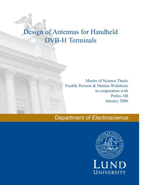
Design of Antennas for Handheld DVB-H ... - Lunds tekniska högskola
Design of Antennas for Handheld DVB-H ... - Lunds tekniska högskola
Design of Antennas for Handheld DVB-H ... - Lunds tekniska högskola

You also want an ePaper? Increase the reach of your titles
YUMPU automatically turns print PDFs into web optimized ePapers that Google loves.
<strong>Design</strong> <strong>of</strong> <strong>Antennas</strong> <strong>for</strong> <strong>Handheld</strong><br />
<strong>DVB</strong>-H Terminals<br />
Master <strong>of</strong> Science Thesis<br />
Fredrik Persson & Mattias Wideheim<br />
in cooperation with<br />
Perlos AB<br />
January 2006<br />
Department <strong>of</strong> Electroscience
Abstract<br />
<strong>DVB</strong>-H is a standard that makes it possible to deliver live broadcast<br />
television to handheld terminals. It is developed from the <strong>DVB</strong>-T standard,<br />
which makes it possible to send <strong>DVB</strong>-H signals along with <strong>DVB</strong>-T signals in<br />
the same multiplexer, in the <strong>DVB</strong>-H/T frequency band 470-862 MHz. A<br />
benefit with this is that it is possible to reuse the <strong>DVB</strong>-T transmission<br />
equipment. The differences between <strong>DVB</strong>-H and <strong>DVB</strong>-T are some additions<br />
that improve the features <strong>for</strong> a mobile terminal in the <strong>DVB</strong>-H standard. The<br />
most important additions are the time slicing, in order to reduce the average<br />
power consumption, and MPE-FEC <strong>for</strong> improving Doppler per<strong>for</strong>mance and<br />
tolerance against interference.<br />
A big challenge in developing terminals <strong>for</strong> the <strong>DVB</strong>-H system is the<br />
antenna. The problem is the low frequencies and the small size <strong>of</strong> today’s<br />
handheld terminals. The result is electrically small antennas that are difficult<br />
to get good efficiency with. The large bandwidth is another big problem<br />
when designing antennas <strong>for</strong> <strong>DVB</strong>-H.<br />
After an introduction <strong>of</strong> the <strong>DVB</strong>-H system this master thesis investigates<br />
different solutions <strong>for</strong> both external and internal antennas <strong>for</strong> the <strong>DVB</strong>-H<br />
system, such as PIFA, loop antenna, monopole and dipole.<br />
The investigation takes RF per<strong>for</strong>mance, size, design, complexity and cost in<br />
consideration when evaluating the proposals <strong>for</strong> <strong>DVB</strong>-H antennas.<br />
I
Acknowledgements<br />
This master thesis is our final thesis at the Master <strong>of</strong> Science programme in<br />
Electrical engineering at Lund institute <strong>of</strong> technology.<br />
To start with we would like to thank our supervisors Anders Sunesson and<br />
Dag Mårtensson <strong>for</strong> giving us the chance to work with this interesting thesis<br />
and all support during the work.<br />
We also would like to thank the entire RF engineer team at Perlos who have<br />
supplied us with technical and antenna knowledge and helped us through a<br />
lot <strong>of</strong> the problems that have turned up during the work. We are also grateful<br />
to all other Perlos employees <strong>for</strong> the pleasant Wednesday meetings.<br />
Finally we would like to thank our supervisor Anders Karlsson at LTH.<br />
This work has been supported and funded by Perlos AB in Lund.<br />
II
List <strong>of</strong> contents<br />
1 INTRODUCTION ..........................................................................................1<br />
1.1 Thesis overview.......................................................................................... 1<br />
1.2 Purpose....................................................................................................... 2<br />
2 BACKGROUND............................................................................................3<br />
2.1 Digital Video Broadcasting....................................................................... 3<br />
2.1.1 <strong>DVB</strong> .................................................................................................... 3<br />
2.1.2 OFDM ................................................................................................. 4<br />
2.1.3 Reed-Solomon Codes.......................................................................... 7<br />
2.1.4 <strong>DVB</strong>-T................................................................................................. 7<br />
2.1.5 <strong>DVB</strong>-H ................................................................................................ 9<br />
2.1.5.1 Standardization <strong>of</strong> <strong>DVB</strong>-H............................................................ 10<br />
2.1.5.2 Time slicing................................................................................... 11<br />
2.1.5.3 Multi Protocol Encapsulation – Forward Error Correction........... 12<br />
2.1.5.4 MPE-FEC frame............................................................................ 13<br />
2.1.5.5 4K mode ........................................................................................ 14<br />
2.1.5.6 Transmission Parameter Signalling - TPS .................................... 15<br />
2.2 Competing standards .............................................................................. 17<br />
2.2.1 Satellite-Digital Mobile Broadcast.................................................... 17<br />
2.2.2 Mobile Broadcast/Multicast Service ................................................. 17<br />
2.3 Antenna theory ........................................................................................ 19<br />
2.3.1 Efficiency, directivity and gain......................................................... 19<br />
2.3.2 Reflection from a mismatched antenna ............................................. 19<br />
2.3.3 Resonance Circuit ............................................................................. 21<br />
2.3.4 Quality Factor.................................................................................... 22<br />
2.3.5 Bandwidth......................................................................................... 23<br />
2.3.5.1 Impedance matching ..................................................................... 23<br />
2.3.6 Bandwidth enhancement ................................................................... 24<br />
3 POSSIBLE SOLUTIONS..........................................................................26<br />
3.1 Dipole and Monopole antenna ............................................................... 26<br />
3.2 Yagi-Uda .................................................................................................. 26<br />
3.3 Loop.......................................................................................................... 27<br />
3.4 Microstrip antenna.................................................................................. 27<br />
III
4 DESIGN AND TESTING OF ANTENNA SOLUTIONS .......................30<br />
4.1 Required antenna per<strong>for</strong>mance ............................................................. 30<br />
4.2 Monopole.......................................................Error! Bookmark not defined.<br />
4.3 Folded dipole antenna ............................................................................. 32<br />
4.4 PIFA.......................................................................................................... 33<br />
4.5 Folded-Patch............................................................................................ 35<br />
4.6 Loop antenna ........................................................................................... 38<br />
4.7 Switched Monopole ................................................................................. 43<br />
5 MEASUREMENTS OF ANTENNA SOLUTION....................................54<br />
5.1 Anechoic chamber measurement ........................................................... 54<br />
5.1.1 Test set-up ......................................................................................... 54<br />
5.1.2 Measurements.................................................................................... 54<br />
5.1.3 Measurement result ........................................................................... 59<br />
5.1.4 Measurement reliability..................................................................... 69<br />
5.2 Testing with <strong>DVB</strong>-T receiver................................................................. 70<br />
6 RESULTS....................................................................................................72<br />
6.1 RF Per<strong>for</strong>mance ...................................................................................... 72<br />
6.2 <strong>Design</strong>....................................................................................................... 72<br />
6.3 Control signal........................................................................................... 73<br />
6.4 Cost........................................................................................................... 73<br />
7 CONCLUSION............................................................................................74<br />
8 REFERENCES............................................................................................79<br />
IV
List <strong>of</strong> figures<br />
Figure 2.1. Multi path propagation <strong>of</strong> the transmitted signal………………….. 6<br />
Figure 2.2. Digital TV standards used in the world……………………………. 8<br />
Figure 2.3. Connection between the specifications defining <strong>DVB</strong>-H.………….10<br />
Figure 2.4. An example <strong>of</strong> the data sent trough one multiplexer……………….12<br />
Figure 2.5. The three elements that <strong>for</strong>m the <strong>DVB</strong>-H codec…………………... 13<br />
Figure 2.6. The MPE-FEC frame……………………………………………….14<br />
Figure 2.7. <strong>DVB</strong>-H symbol interleaving scheme……………………………….15<br />
Figure 2.8. Voltage reflection from a mismatched load……………………….. 19<br />
Figure 2.9. Impedance bandwidth………………………………………………21<br />
Figure 2.10. Parallel resonance circuit………………………………………….22<br />
Figure 2.11. Matching circuit scheme…………………………………………..24<br />
Figure 3.1. Yagi-Uda antenna………………………………………………...... 27<br />
Figure 3.2. Four different configurations to feed microstrip antennas………….29<br />
Figure 3.3. PIFA antenna………………………………………………………. 29<br />
Figure 4.1. Specified gain <strong>for</strong> handheld <strong>DVB</strong>-T terminals……………………..30<br />
Figure 4.2. Dipole antenna……………………………………………………... 32<br />
Figure 4.3. Dipole antenna dimensions………………………………………....32<br />
Figure 4.4. Dipole antenna, return loss graph………………………………….. 33<br />
Figure 4.5. PIFA antenna………………………………………………………. 34<br />
Figure 4.6. PIFA return loss graph…………………………………………….. 34<br />
Figure 4.7. Folded-patch antenna……………………………………………….35<br />
Figure 4.8. Return loss graph <strong>for</strong> the folded-patch…………………………….. 36<br />
Figure 4.9. Folded-patch 2 antenna……………………………………………..37<br />
Figure 4.10. Return loss graph <strong>of</strong> the folded-patch 2………………..….………38<br />
Figure 4.11. Loop antenna schematic………………………………………….. 39<br />
Figure 4.12. Perlos loop antenna………………...……………………………...39<br />
Figure 4.13. Perlos loop antenna return loss graph……………………………..40<br />
Figure 4.14. Wire loop antenna…………………………………………………40<br />
Figure 4.15. Wire loop antenna return loss graph………………………………41<br />
Figure 4.16. Loop antenna…………………………………………………….. 42<br />
Figure 4.17. Loop antenna return loss graph………………………………….. 42<br />
Figure 4.18. Model <strong>of</strong> switched monopole concept…………………………….43<br />
Figure 4.19. Example <strong>of</strong> four different matching circuits……………………... 44<br />
Figure 4.20. Switched monopole without RF switches………………………... 44<br />
Figure 4.21. Schematic <strong>for</strong> four matching……………………………………... 45<br />
Figure 4.22. Return loss Graph <strong>for</strong> switched monopole……………………….. 46<br />
Figure 4.23. Switched monopole 2…………………………………………….. 48<br />
Figure 4.24. Return loss graph - circuit 1, switched monopole 1……………… 49<br />
Figure 4.25. Return loss graph - circuit 2, switched monopole 1……………… 49<br />
Figure 4.26. Return loss graph - circuit 3, switched monopole 1……………… 50<br />
Figure 4.27. Return loss graph - circuit 4, switched monopole 1……………… 50<br />
Figure 4.28. Return loss graph - circuit 1, switched monopole 2……………… 51<br />
Figure 4.29. Return loss graph - circuit 2, switched monopole 2……………… 52<br />
Figure 4.30. Return loss graph - circuit 3, switched monopole 2……………… 52<br />
Figure 4.31. Return loss graph - circuit 4, switched monopole 2....…………… 53<br />
Figure 5.1. Schematic view <strong>of</strong> Perlos anechoic chamber……………………… 54<br />
V
Figure 5.2. Reference dipole antenna………………………………………….. 55<br />
Figure 5.3. Reference dipole antenna return loss graph……………………….. 55<br />
Figure 5.4. Radiation pattern <strong>for</strong> Reference antenna………………………….. 56<br />
Figure 5.5. Radiation pattern <strong>for</strong> Reference antenna………………………….. 56<br />
Figure 5.6. Radiation pattern <strong>for</strong> Reference antenna………………………….. 57<br />
Figure 5.7. Gain <strong>for</strong> the folded-patch 1 verses specification………………….. 59<br />
Figure 5.8. Radiation pattern <strong>for</strong> Folded-patch 1……………………………….60<br />
Figure 5.9. Radiation pattern <strong>for</strong> Folded-patch 1……………………………….60<br />
Figure 5.10. Radiation pattern <strong>for</strong> Folded-patch 1………………..…………….61<br />
Figure 5.11. Gain <strong>for</strong> five different capacitances in the loop antenna…………. 61<br />
Figure 5.12. Radiation pattern <strong>for</strong> Loop antenna………………………………. 63<br />
Figure 5.13. Radiation pattern <strong>for</strong> Loop antenna………………………………. 63<br />
Figure 5.14. Radiation pattern <strong>for</strong> Loop antenna………………………………. 64<br />
Figure 5.15. Gain <strong>for</strong> the different circuits, switched monopole 1…………….. 64<br />
Figure 5.16. Radiation pattern <strong>for</strong> Switched monopole 1……………………… 65<br />
Figure 5.17. Radiation pattern <strong>for</strong> Switched monopole 1……………………… 66<br />
Figure 5.18. Radiation pattern <strong>for</strong> Switched monopole 1……………………… 66<br />
Figure 5.19. Gain <strong>for</strong> the different circuits, switched monopole 2…………….. 67<br />
Figure 5.20. Radiation pattern <strong>for</strong> Switched monopole 2……………………… 68<br />
Figure 5.21. Radiation pattern <strong>for</strong> Switched monopole 2……………………… 68<br />
Figure 5.22. Radiation pattern <strong>for</strong> Switched monopole 2……………………… 69<br />
VI
List <strong>of</strong> tables<br />
Table 2.1. Qualities <strong>for</strong> the three different modes……………………….…….. 15<br />
Table 2.2. The TPS block……………………………………………………… 16<br />
Table 4.1. Value <strong>of</strong> components <strong>for</strong> the different switched monopoles……….. 45<br />
Table 5.1. Reference antenna values <strong>for</strong> calculation <strong>of</strong> gain and efficiency…... 58<br />
Table 5.2. Folded-patch 1 gain and efficiency results…………………………. 59<br />
Table 5.3. Loop antenna, gain and efficiency results………………………….. 62<br />
Table 5.4. Switched monopole 1, gain and efficiency results…………………. 65<br />
Table 5.5. Switched monopole 2, gain and efficiency results…...…………….. 67<br />
VII
1 Introduction<br />
The passed decade the media consumption has grown rapidly. Devices like video<br />
recorders, video-on-demand and pay-per view <strong>of</strong>ferings have enabled users to<br />
personalize the content they want to watch. Today the majority <strong>of</strong> the European<br />
population has access to Internet and a large number <strong>of</strong> TV-channels.<br />
Along with this trend is the amazing development <strong>of</strong> mobile telephones. Mobile<br />
terminals are packed with new technologies that broaden their functionality. The<br />
mobile terminal converges and can be used as an organizer, game console, music<br />
player, portable radio, agenda, camera, video camera and now, television. The<br />
place <strong>of</strong> viewing is no longer limited to a television set at home or in a vehicle.<br />
Instead, it is widened to allow personal viewing <strong>of</strong> television anytime at anyplace.<br />
Television has been brought to mobiles through the use <strong>of</strong> cellular networks.<br />
However, providing television this way is very expensive and if many users want<br />
to watch the same channel at the same time a lot <strong>of</strong> bandwidth will be used to<br />
send the same in<strong>for</strong>mation over and over again.<br />
Digital Video Broadcasting – <strong>Handheld</strong> (<strong>DVB</strong>–H) is a standard that makes it<br />
possible to deliver live broadcast television to handheld terminals. There are other<br />
standards that are competing with <strong>DVB</strong>-H to be the main television provider in<br />
Europe. All the technical problems with the <strong>DVB</strong>-H standard have not yet been<br />
solved. If <strong>DVB</strong>-H is to be the main television provider in Europe these technical<br />
problems need to be solved rather quickly. We believe they will be solved and<br />
that the <strong>DVB</strong>-H standard is the best way to provide television <strong>for</strong> mobile<br />
terminals.<br />
1.1 Thesis overview<br />
Chapter 2 <strong>of</strong> this thesis introduces the <strong>DVB</strong>-H system. It also has one part about<br />
competing standards and the last part <strong>of</strong> this chapter is an introduction <strong>of</strong> antenna<br />
theory that is related to this work.<br />
Chapter 3 gives an overview <strong>of</strong> existing antenna solutions <strong>for</strong> the <strong>DVB</strong>-H<br />
frequencies. Chapter 4 describes the design <strong>of</strong> all our solutions with return loss<br />
graphs and characteristics <strong>for</strong> the different antennas. In chapter 5 the three final<br />
prototypes are presented and different measurements on these are presented.<br />
Chapter 6 contains the results from all measurements and chapter 7 is <strong>for</strong> final<br />
conclusions.<br />
1
1.2 Purpose<br />
This thesis has a couple <strong>of</strong> purposes. In the beginning the work is completely<br />
theoretical and the objective is to collect as much in<strong>for</strong>mation as possible about<br />
the <strong>DVB</strong>-H system and summarize this in<strong>for</strong>mation in the report. It is important to<br />
understand the possibilities and limits that <strong>DVB</strong>-H <strong>of</strong>fers. The goal is to extract an<br />
antenna specification <strong>for</strong> handheld devices on the basis <strong>of</strong> the obtained<br />
in<strong>for</strong>mation.<br />
When this theoretical part is done the goal is to design some <strong>DVB</strong>-H antennas and<br />
make measurements on them. The measurements that will be presented <strong>for</strong> these<br />
antennas are power gain, efficiency, radiation pattern and interference<br />
measurements.<br />
The most important purpose <strong>of</strong> this thesis is to create a knowledge plat<strong>for</strong>m that<br />
makes it easier to design antennas <strong>for</strong> <strong>DVB</strong>-H in the future.<br />
2
2 Background<br />
This chapter provides general in<strong>for</strong>mation about the different <strong>DVB</strong> standards and<br />
will give the needed knowledge about the system. Basic antenna theory will also<br />
be presented, to help the reader understand later discussions.<br />
2.1 Digital Video Broadcasting<br />
2.1.1 <strong>DVB</strong><br />
This part will give the reader an overview <strong>of</strong> the existing Digital Video<br />
Broadcasting – Terrestrial (<strong>DVB</strong>-T) system and the future <strong>DVB</strong>-H system.<br />
The analogue TV system used today has basically remained unchanged <strong>for</strong><br />
decades, with the colour TV as the only invention worth mentioning since the<br />
1960s. The European PAL system and the US NTSC system use the resolution <strong>of</strong><br />
625 lines respectively 525 lines, and the display is interlaced with only 25 or 30<br />
frames per second. Compared with today’s computer screen with resolution <strong>of</strong><br />
1280�1024 and at least 75 Hz frame rate. So, it is naturally that a transition to a<br />
digital system with higher resolution implies better picture and additional features<br />
[1].<br />
Until 1991 digital television broadcasting to the home was thought expensive and<br />
impractical to implement. During 1991 broadcasters and equipment manufactures<br />
discussed unify Europe with one standard <strong>for</strong> digital TV. The result was a group<br />
called European Launching Group (ELG) that expanded to include the major<br />
European media interest groups, both public and private, the consumer electronics<br />
manufacturers, common carriers and regulators. 1993 ELG renamed itself to<br />
Digital Video Broadcasting (<strong>DVB</strong>). The work in digital television, already<br />
underway in Europe, moved into top gear. It became clear that Digital Video<br />
Broadcasting–Satellite (<strong>DVB</strong>-S) and Digital Video Broadcasting–Cable (<strong>DVB</strong>-C)<br />
were delivering digital video broadcasting be<strong>for</strong>e <strong>DVB</strong>-T. This depends on fewer<br />
technical problems and a simpler regulatory.<br />
1997 the <strong>DVB</strong>-standards were adopted globally and became the benchmark <strong>for</strong><br />
digital television worldwide [2].<br />
<strong>DVB</strong> is an industry-led group with more than 300 broadcasters, manufacturers,<br />
network operators, s<strong>of</strong>tware developers and regulatory bodies. One <strong>of</strong> the main<br />
goals <strong>for</strong> the group is to develop open standards to prevent the digital TV to<br />
include as many standards as the analogue system (NTSC, PAL and SECAM)<br />
does. Since European Telecommunication Standards Institute (ETSI) adopted<br />
<strong>DVB</strong> as a standard, it has been implemented in many countries. An EU directive<br />
requires all country which will implement digital terrestrial TV broadcasting to<br />
3
2.1.2 OFDM<br />
choose <strong>DVB</strong>. But <strong>DVB</strong> is not the only standard <strong>for</strong> digital broadcast in the world,<br />
e.g. Japan has developed Integrated Services Digital Broadcasting - Terrestrial<br />
(ISDB-T) and in US they have implemented Advanced Television System<br />
Committee (ATSC) [3].<br />
One <strong>of</strong> the best things with the digital system compared to the analogue is the<br />
spectrum efficiency. It is possible to send four to six digital channels by the<br />
multiplex instead <strong>of</strong> one analogue channel on the same frequency. The <strong>DVB</strong>standard<br />
uses the video <strong>for</strong>mat MPEG-2 while the sound is coded with MPEG-1,<br />
layer II. Normally 80 percent <strong>of</strong> the capacity is reserved <strong>for</strong> the video stream and<br />
10 percent each <strong>for</strong> the sound and teletext [4].<br />
Orthogonal Frequency Division Multiplexing (OFDM) was developed in 1960,<br />
but it has not been used much until lately. It has become very popular because it is<br />
now possible to build the integrated circuits that are needed to per<strong>for</strong>m the highspeed<br />
digital operations necessary <strong>for</strong> OFDM. It is based on Frequency Division<br />
Multiplexing (FDM), which is a technology that uses multiple frequencies to<br />
simultaneously transmit multiple signals in parallel [5].<br />
It is different to transmit a terrestrial broadcasting channel than to transmit a<br />
satellite link or a cable transmission channel. You will get reflections from<br />
buildings and mountains, which will result in a multi path propagation <strong>of</strong> the<br />
transmitted signal (See figure 2.1). These reflected signals will be time-delayed at<br />
the receiver and can cause harmful interference. If the delay time <strong>of</strong> the echo<br />
signals is in the range <strong>of</strong> the symbol duration <strong>of</strong> the transmitted signal it will result<br />
in a selective behaviour <strong>of</strong> the frequency response [6].<br />
The individual echoes which successively arrive at the receiver, vary in amplitude<br />
and delay time. By superimposing themselves on the main signal they cause<br />
fluctuations in the complex channel transfer function. A characteristic value <strong>of</strong><br />
such fading channels is given by the ratio <strong>of</strong> the directly received signal power to<br />
the total <strong>of</strong> the power <strong>of</strong> all echo signals [7].<br />
It is possible to compensate <strong>for</strong> the distortions in the frequency domain by using<br />
suitable equalizers. Usually the time delay <strong>of</strong> the echo exceeds the symbol<br />
duration. This means that the adjacent symbols affect each other. A filter <strong>for</strong> inter<br />
symbol interference must there<strong>for</strong>e be <strong>of</strong> a high order, which is hard and<br />
expensive to implement.<br />
To minimize the number <strong>of</strong> symbols affecting each other you can just make the<br />
duration <strong>of</strong> the transmitted symbol longer. This can be done by the parallel<br />
transmission <strong>of</strong> several symbols. If, <strong>for</strong> instance, the in<strong>for</strong>mation to be transmitted<br />
4
is simultaneously modulated into 1000 symbols <strong>of</strong> different carrier frequencies,<br />
then <strong>for</strong> each individual symbol there is a time slot available, which be<strong>for</strong>e<br />
changing to parallel transmission, was allotted to all the sequentially transmitted<br />
symbols together. The value <strong>of</strong> the bandwidth and the transmission time <strong>of</strong> some<br />
in<strong>for</strong>mation can vary as a function <strong>of</strong> each other. If OFDM is used to send a<br />
symbol the frequency range required <strong>for</strong> the transmission <strong>of</strong> an individual<br />
subsymbol is reduced [6].<br />
In the OFDM system all the subcarrier frequencies should be orthogonal to each<br />
other. To get the subcarriers to be orthogonal to each other the Inverse Discrete<br />
Fourier Trans<strong>for</strong>m (IDFT) must be calculated. It is necessary <strong>for</strong> a predetermined<br />
number <strong>of</strong> subsymbols to be available simultaneously at the input <strong>of</strong> the IDFT<br />
unit. The data that are to be transmitted are temporarily stored until the required<br />
number <strong>of</strong> subsymbols <strong>for</strong> parallel transmission are ready to be sent, and are then<br />
read out in parallel.<br />
One <strong>of</strong> the major problems <strong>of</strong> OFDM is that the peak amplitude <strong>of</strong> the emitted<br />
signal can be considerably higher than the average amplitude. This Peak to<br />
Average Ratio (PAR) problem comes from the fact that an OFDM signal is the<br />
superposition <strong>of</strong> all the sinusoidal signals <strong>of</strong> the different subcarriers. On average<br />
the emitted power is linearly proportional to the number <strong>of</strong> carriers. Sometimes<br />
the signals on the subcarriers ad up constructively and then the amplitude <strong>of</strong> the<br />
signal is proportional to the number <strong>of</strong> carriers. There are three ways <strong>of</strong> dealing<br />
with this:<br />
1. Use a power amplifier in the transmitter that can amplify linearly up to the<br />
possible peak value. This solution requires expensive and power<br />
consuming class A amplifiers.<br />
2. Use a nonlinear amplifier, and accept that the amplifier characteristic will<br />
lead to distortions <strong>of</strong> the output signal. Those nonlinear distortions destroy<br />
the orthogonality between the subcarriers, and also leads to out <strong>of</strong> band<br />
emissions.<br />
3. Use PAR reduction techniques. There are several different approaches<br />
these will not be described in this rapport.<br />
5
Figure 2.1. Multi path propagation <strong>of</strong> the transmitted signal.<br />
The OFDM transmission scheme has the following key advantages:<br />
• Makes efficient use <strong>of</strong> the spectrum by allowing overlap.<br />
• By dividing the channel into narrowband flat fading subchannels, OFDM<br />
is more resistant to frequency selective fading than single carrier systems<br />
are.<br />
• Eliminates ISI and IFI through use <strong>of</strong> a cyclic prefix.<br />
• Using adequate channel coding and interleaving one can recover symbols<br />
lost due to the frequency selectivity <strong>of</strong> the channel.<br />
• Channel equalization becomes simpler than by using adaptive equalization<br />
techniques with single carrier systems.<br />
• In conjunction with differential modulation there is no need to implement<br />
a channel estimator.<br />
• Is less sensitive to sample timing <strong>of</strong>fsets than single carrier systems are.<br />
• Provides good protection against co-channel interference and impulsive<br />
parasitic noise.<br />
In terms <strong>of</strong> drawbacks OFDM has the following characteristics:<br />
• The OFDM signal has a noise like amplitude with a very large dynamic<br />
range, there<strong>for</strong>e it requires RF power amplifiers with a high peak to<br />
average power ratio.<br />
• It is more sensitive to carrier frequency <strong>of</strong>fset and drift than single carrier<br />
systems are due to leakage <strong>of</strong> the DFT [8].<br />
6
2.1.3 Reed-Solomon Codes<br />
2.1.4 <strong>DVB</strong>-T<br />
Reed-Solomon codes (RS codes) are block-based error correcting codes and are<br />
very widely used in digital communications and storage. RS codes can detect and<br />
correct errors within blocks <strong>of</strong> data and are used in a lot <strong>of</strong> applications, <strong>for</strong><br />
example:<br />
• Storage devices (including tape, compact, DVD, barcodes, etc)<br />
• Wireless or mobile communications (including cellular telephones,<br />
microwave links, etc)<br />
• Satellite communications<br />
• Digital television / <strong>DVB</strong><br />
• High-speed modems such as ADSL, xDSL,etc<br />
The RS encoder takes a block <strong>of</strong> digital data and adds extra "redundant" bits.<br />
Errors occur during transmission or storage <strong>for</strong> a number <strong>of</strong> reasons (<strong>for</strong> example<br />
noise or interference, scratches on a CD, etc). The Reed-Solomon decoder<br />
processes each block and attempts to correct errors and recover the original data.<br />
<strong>DVB</strong>-H uses RS (255,191), were 191 is the number <strong>of</strong> in<strong>for</strong>mation symbols input<br />
per block and 255 the number <strong>of</strong> symbols per block that the encoder outputs, the<br />
code rate can be varied. The term symbol may represent one bit or a number <strong>of</strong><br />
bits. The number and type <strong>of</strong> errors that can be corrected depends on the<br />
characteristics <strong>of</strong> the Reed-Solomon code and is always half <strong>of</strong> the parity<br />
symbols. So in the <strong>DVB</strong>-H system it is possible to correct up to 32 errors in a<br />
codeword [9].<br />
<strong>DVB</strong>-T is the terrestrial mode <strong>for</strong> Digital Video Broadcasting. <strong>DVB</strong>-T has been<br />
selected as the common standard <strong>for</strong> digital television in Europe and is the base<br />
plat<strong>for</strong>m <strong>for</strong> <strong>DVB</strong>-H, witch makes it possible to transmit IP-packages to handheld<br />
terminals. The standard <strong>for</strong> <strong>DVB</strong>-T was adopted in December 1995. In November<br />
1998 the first <strong>DVB</strong>-T network became operational in the United Kingdom. Since<br />
1998 <strong>DVB</strong>-T has been introduced in Europe, Australia, Singapore and Taiwan [6].<br />
See figure 2.2 to see the spread <strong>of</strong> the different digital TV specifications.<br />
In <strong>DVB</strong>-T, each program is sent over a separate logical channel that is identified<br />
by a unique packet identifier. All users that have access to a specific service may<br />
receive any program on that logical channel. The control streams used with the<br />
packet identifiers such as the program and service in<strong>for</strong>mation are transmitted<br />
repeatedly from the head end to the users [10].<br />
7
Usually the Moving Pictures Experts Group (MPEG-2) compression code is used<br />
to compress <strong>DVB</strong>-T transmissions. However the latest <strong>DVB</strong>-T specification<br />
allows AVC/H.264 as a compliment.<br />
<strong>DVB</strong>-T divides the signal into several thousand orthogonal subcarriers using<br />
ODFM. The system is designed to operate with the Ultra High Frequency (UHF)<br />
spectrum, and can be used with 6, 7 or 8 MHz channel bandwidths depending on<br />
the regional demands. <strong>DVB</strong>-T has many parameters that can be changed to best<br />
fulfill the regions needs. The parameters that can be changed are the number <strong>of</strong><br />
subcarriers, guard interval, whether a hierarchical signal is used, error correction<br />
level and the modulation scheme. The number <strong>of</strong> subcarriers used affects what<br />
Doppler frequency the system can handle and what range it can cover. The<br />
Doppler frequency is the shift in frequency and wavelengths depending on what<br />
speed the terminal have. <strong>DVB</strong>-T has two modes that determine the number <strong>of</strong><br />
subcarriers, 2k and 8k. The guard interval parameter determines the signal’s<br />
tolerance to echo. Because the system has this ability to tolerate echo it is possible<br />
to use the spectrum efficient Single Frequency Networks (SFN). A SFN is a<br />
network <strong>of</strong> several stations that broadcast the same signal simultaneously using<br />
multiple transmitters [11].<br />
Today <strong>DVB</strong>-T is more effective than its initial requirements. For example <strong>DVB</strong>-T<br />
can be used in public transportations and in cars. It is also possible to <strong>of</strong>fer IPdatacasting<br />
over the <strong>DVB</strong>-T network even though this network was not designed<br />
to target mobile handset. The problem with IP-datacasting over the <strong>DVB</strong>-T<br />
network is the battery consumption.<br />
Figure 2.2. Digital TV standards used in the world.<br />
8
2.1.5 <strong>DVB</strong>-H<br />
<strong>DVB</strong>-H is the latest developed standard within the <strong>DVB</strong> transmission standards.<br />
The work with the technical specification started in autumn 2002 and was finished<br />
in February 2004. In November the same year ETSI finally published the <strong>DVB</strong>-H<br />
standard as a European Norm [12].<br />
The first step towards <strong>DVB</strong>-H was taken when the ability <strong>of</strong> <strong>DVB</strong>-T to deliver<br />
broadcast services to mobile receivers was demonstrated.<br />
The problem was the power consumption, and that lead to the new standard,<br />
<strong>DVB</strong>-H that enables IP datacasting. IP datagrams that are broadcasted over <strong>DVB</strong>-<br />
H are encapsulated inside the MPEG-2 transport stream using the Multi Protocol<br />
Encapsulation (MPE) to improve mobile per<strong>for</strong>mance [11].<br />
<strong>DVB</strong>-H is so similar to <strong>DVB</strong>-T that it is possible to send <strong>DVB</strong>-H signals along<br />
with <strong>DVB</strong>-T signals in the multiplexer, between 470 – 862 MHz [4]. That it is<br />
possible to reuse <strong>DVB</strong>-T transmission equipment makes it an interesting<br />
technique in an economically point <strong>of</strong> view. <strong>DVB</strong>-H has a downstream channel<br />
with capacity <strong>of</strong>f several Mbit/s. It may be used <strong>for</strong> radio and video streaming, file<br />
downloads and many other applications.<br />
<strong>DVB</strong>-H includes the following additions to improve the features <strong>for</strong> a mobile<br />
terminal:<br />
• Time slicing, in order to reduce the average power consumption <strong>of</strong> the<br />
terminal and to make it possible to smooth handovers.<br />
• MPE-FEC, <strong>for</strong> improving Doppler per<strong>for</strong>mance and tolerance to impulse<br />
interference.<br />
• 4k-mode, provides more flexibility to network design.<br />
• In-depth symbol interleaver, <strong>for</strong> further improvement <strong>of</strong> the transmitted<br />
signal robustness in mobile environment.<br />
• Extended Transmission Parameter Signaling (TPS).<br />
The <strong>DVB</strong>-H standard recommends using H.264 (MPEG-4 Part 10: Advanced<br />
Video Codec) and the CIF resolution (352*288) in difference to <strong>DVB</strong>-T that uses<br />
MPEG-2 code and SDTV (720*576) [14]. During 2004 and 2005 successful trials<br />
have been going on in Helsinki, Berlin and Pittsburg.<br />
Several European countries have plans to launch commercial services already<br />
2006, and according to market prospects, the sales figures will be somewhere<br />
between 10 and 100 millions 2008 [15]<br />
9
2.1.5.1 Standardization <strong>of</strong> <strong>DVB</strong>-H<br />
The <strong>DVB</strong>-H system is not specified in one single document. Instead some<br />
modifications to other <strong>DVB</strong> specifications have been made (See figure 2.3).<br />
• The central specification is the <strong>DVB</strong>-H system specification EN 302 304.<br />
It has been published as the European norm <strong>for</strong> <strong>DVB</strong>-H.<br />
• The physical layer specification has been integrated in the <strong>DVB</strong>-T<br />
specification EN 300 744. This standard has been published as a new<br />
version, which contains the <strong>DVB</strong>-H physical layer enhancements in an<br />
annex.<br />
• Time slicing and MPE-FEC have been described in a new chapter <strong>of</strong> the<br />
<strong>DVB</strong> Data Broadcast specification EN 301 192. This document also<br />
defines the Multi-Protocol Encapsulation.<br />
• <strong>DVB</strong>-H-specific signaling has been integrated into the <strong>DVB</strong> Service<br />
In<strong>for</strong>mation (SI) specification EN 300 468.<br />
Figure 2.3. The connection between the different specifications defining <strong>DVB</strong>-H.<br />
The system specification determines mandatory and optional elements. The<br />
system specification is complemented by <strong>DVB</strong>-H implementation guidelines,<br />
which contain hints <strong>for</strong> the use and practical implementation <strong>of</strong> the standard. The<br />
<strong>DVB</strong> Project released these guidelines in the autumn <strong>of</strong> 2004 [12].<br />
10
2.1.5.2 Time slicing<br />
A large problem with handheld terminals is the limited battery capacity. It is<br />
impossible to receive and decode a broad band, high data-rate stream like the<br />
<strong>DVB</strong>-T data stream with a battery terminal. The receiver and demodulation part in<br />
the terminal would use too much power and the battery would run out quickly. In<br />
the beginning <strong>of</strong> the development <strong>of</strong> <strong>DVB</strong>-H it was shown that the power<br />
consumption <strong>of</strong> a <strong>DVB</strong>-T receiver is about 1 Watt, which is too much [14]. A<br />
some-what lower value seems possible but the desired target <strong>of</strong> 100 mW as a<br />
maximum threshold <strong>for</strong> the entire front end incorporated in a <strong>DVB</strong>-H terminal is<br />
still unobtainable <strong>for</strong> a <strong>DVB</strong>-T receiver.<br />
A considerable drawback <strong>for</strong> battery-operated terminals is the fact that with <strong>DVB</strong>-<br />
T, the whole data stream has to be decoded be<strong>for</strong>e any one <strong>of</strong> the services (TV<br />
programs) <strong>of</strong> the multiplex can be accessed. The main reason why <strong>DVB</strong>-H<br />
consumes less power is that the receiver only has to receive and process the parts<br />
<strong>of</strong> the data stream that contains the in<strong>for</strong>mation needed <strong>for</strong> the selected service.<br />
For this to be possible the data stream needs to be reorganized in a suitable way.<br />
With <strong>DVB</strong>-H, service multiplexing is per<strong>for</strong>med in a pure time-division<br />
multiplex. The data <strong>of</strong> one particular service are there<strong>for</strong>e not transmitted<br />
continuously but in compact periodical bursts with interruptions in between. In the<br />
interruption between bursts, other services are sent. This leads to a continuous<br />
data stream. This data stream can be received in time intervals where the receiver<br />
is synchronized with the service you want to receive. Then the receiver can be<br />
shut down when the other services that you have no interest in are sent. This way<br />
<strong>of</strong> dividing the signal is called time slicing [15].<br />
When time slicing is used to receive the signal it saves a lot <strong>of</strong> power because the<br />
receiver can be turned <strong>of</strong>f most <strong>of</strong> the time. When the receiver is on, the received<br />
signal is buffered in a memory and then read out from the buffer in the service<br />
data-rate. When the receiver is turned on the next time and receives a new data<br />
stream, this data is buffered in the memory and the video can be played<br />
continuously. For the receiver to know when it is time to turn itself on again after<br />
an <strong>of</strong>f-time, data containing in<strong>for</strong>mation about how long the receiver should be<br />
turned <strong>of</strong>f between the bursts, has to be sent in each burst.<br />
The duration <strong>of</strong> one burst is in the range <strong>of</strong> several hundred milliseconds whereas<br />
the power save time may amount to several seconds. The receiver has to be turned<br />
on be<strong>for</strong>e it is time to receive data and there<strong>for</strong>e it is turned on 50-250 ms be<strong>for</strong>e<br />
calculated receiving time. Depending on the ratio between on time and <strong>of</strong>f time,<br />
the resulting power saving may be more than 90 %.<br />
As an example, figure 2.4 shows a cut-out <strong>of</strong> a data stream containing time-sliced<br />
services. One quarter <strong>of</strong> the assumed total capacity <strong>of</strong> the <strong>DVB</strong>-T channel <strong>of</strong><br />
11
13.27 Mbit/s is assigned to <strong>DVB</strong>-H services whereas the remaining capacity is<br />
shared between ordinary <strong>DVB</strong>-T services. This example shows that it is possible<br />
to transmit both <strong>DVB</strong>-T and <strong>DVB</strong>-H within the same network.<br />
Another benefit with time slicing is that the receiver is able to search <strong>for</strong> the<br />
service in use in other cells during the receiver’s <strong>of</strong>f time. In this way a channel<br />
handover can be per<strong>for</strong>med at the border between two cells without the user<br />
knowing anything about it [6].<br />
Figure 2.4. An example <strong>of</strong> the data sent trough one multiplexer.<br />
2.1.5.3 Multi Protocol Encapsulation – Forward Error Correction<br />
<strong>Handheld</strong> devices with small antennas make the reception <strong>of</strong> high data rate<br />
streams in mobile environment unreliable and difficult. Because <strong>of</strong> that Multi<br />
Protocol Encapsulation – Forward Error Correction (MPE-FEC) was added to the<br />
<strong>DVB</strong>-H standard to improve the C/N- and Doppler per<strong>for</strong>mance in mobile<br />
channels and to improve the tolerance against impulse interference [16]. The use<br />
<strong>of</strong> MPE-FEC is optional.<br />
In contrast to other <strong>DVB</strong> transmission systems based on the <strong>DVB</strong> transport stream<br />
adopted from the MPEG-2 standard, the <strong>DVB</strong>-H system is based on Internet<br />
Protocol (IP). There<strong>for</strong>e is the base-band interface an IP interface, this interface<br />
allows the <strong>DVB</strong>-H system to be combined with other IP networks. The MPEG-2<br />
transport stream is still used, because the IP data are embedded into the transport<br />
stream by means <strong>of</strong> the Multi Protocol Encapsulation (MPE), a protocol defined<br />
by <strong>DVB</strong> Data Broadcast Specification. On the same level as MPE is an additional<br />
Forward Error Correction (FEC) added. This technique is called MPE-FEC and is<br />
the second main innovation besides time slicing [15]. Intensive testing <strong>of</strong> <strong>DVB</strong>-H,<br />
by <strong>DVB</strong> member companies showed that use <strong>of</strong> MPE-FEC improves the result by<br />
7 dB over <strong>DVB</strong>-T [12].<br />
The MPE-FEC scheme is located on the link layer at the level <strong>of</strong> input IP streams<br />
be<strong>for</strong>e they are encapsulated by means <strong>of</strong> the MPE. The MPE, MPE-FEC and<br />
time slicing techniques are neighboring in the transmitter block diagram (See<br />
12
figure 2.5). All three elements together <strong>for</strong>m the <strong>DVB</strong>-H codec, which contain the<br />
essential <strong>DVB</strong>-H functionality.<br />
The input IP streams coming from different sources as single elementary streams<br />
are multiplexed one by one according to the time slicing method. The MPE-FEC<br />
error protection is calculated and added separately <strong>for</strong> each single elementary<br />
stream be<strong>for</strong>e they are encapsulated into the transport stream. All data processing<br />
is carried out be<strong>for</strong>e the transport stream interface to guarantee compatibility to a<br />
<strong>DVB</strong>-T transmission network [15, 30].<br />
2.1.5.4 MPE-FEC frame<br />
Figure 2.5. The three elements that <strong>for</strong>m the <strong>DVB</strong>-H codec.<br />
The MPE-FEC scheme consists <strong>of</strong> RS code in conjunction with a block<br />
interleaver. The MPE-FEC encoder creates a specific MPE-FEC frame (See figure<br />
2.6). In that frame are all <strong>DVB</strong>-H coded input data inserted. The frame consists <strong>of</strong><br />
255 columns and a maximum <strong>of</strong> 1024 rows and with every cell equivalent to one<br />
byte, the maximum frame size is almost 2 Mbit.<br />
A frame is divided in two parts, the application data table and the RS data table.<br />
The application data table is the 191 columns to the left and is filled with the IP<br />
packets <strong>of</strong> the service to be protected. The first byte <strong>of</strong> the first datagram inserts in<br />
the upper left cell and going downwards the first column. If a datagram is longer<br />
than a column it continues on top <strong>of</strong> the next column.<br />
With the application data table filled with datagrams or zero padding it is possible<br />
to calculate the 64 Parity bytes in the RS data table <strong>for</strong> each row with RS<br />
(255,191) code. When the application data table is filled with IP packets and RS<br />
data table with parity bits the MPE-FEC frame is ready <strong>for</strong> transmission [17]. The<br />
IP packets are read out <strong>of</strong> the application data table and encapsulated in IP<br />
sections by means <strong>of</strong> the MPE method. The IP data is carried in MPE sections<br />
irrespective MPE-FEC is used or not. This makes reception backwards compatible<br />
with MPE-FEC ignorant receiver.<br />
13
Every section has in<strong>for</strong>mation in the header about start address <strong>for</strong> the IP<br />
datagram. The address indicates the position <strong>for</strong> the first byte <strong>of</strong> the IP datagram<br />
in the application table. This application data is followed by the parity bytes in the<br />
RS data table that are read out column by column and encapsulated in separate<br />
MPE-FEC sections. The FEC frame structure also contains a block interleaving<br />
effect in addition to coding. That means that the receiver can put the datagram in<br />
right order in the application table and mark it “reliable” <strong>for</strong> the RS decoder. A<br />
flag marks the end <strong>of</strong> the application data table. If all application data is received<br />
correctly none <strong>of</strong> the MPE-FEC sections are necessary. That is optimal if time<br />
slicing is used, because then the receiver can go to sleep [17].<br />
2.1.5.5 4K mode<br />
Figure 2.6. The MPE-FEC frame.<br />
<strong>DVB</strong>-T provides two different modes <strong>for</strong> different topologies, 2K and 8K mode.<br />
<strong>DVB</strong>-H also disposes <strong>of</strong> an intermediate 4K mode that has a little <strong>of</strong> both 2K and<br />
8K modes qualities. The qualities <strong>of</strong> the different modes can be seen in Table 2.1.<br />
It allows twice as long distance between receiver and transmitter in SFNs<br />
compared to the 2K mode and it is less susceptible to Doppler frequencies in case<br />
<strong>of</strong> mobile reception compared to the 8K mode. The 4K mode shall make the<br />
network planning <strong>for</strong> <strong>DVB</strong>-H easier, this does not apply <strong>for</strong> <strong>DVB</strong>-T since it does<br />
not include the 4K mode [10].<br />
To make transmissions with the 4K mode possible a new symbol interleaver with<br />
4096 OFDM carrier frequencies was specified. In connection with the three<br />
network modes a new symbol-interleaving scheme is defined (See figure 2.7). A<br />
<strong>DVB</strong>-H terminal should support all three modes and then needs an 8K symbol<br />
interleaver. It is preferred to use the relatively big memory <strong>of</strong> the 8K symbol<br />
interleaver in all three network modes. This symbol interleaver is able to process<br />
the amount <strong>of</strong> one complete 8K OFDM symbol or alternatively two 4K OFDM<br />
14
symbols or four 2K OFDM symbols. This way the memory is used more<br />
effectively and it results in an increased interleaving depth in the 2K and 4K<br />
modes, which can be expected to improve per<strong>for</strong>mance. If the full memory<br />
interleaving solution is used it is called in-depth interleaving [15].<br />
Table 2.1. Qualities <strong>for</strong> the three different modes.<br />
Mode<br />
OFDM parameter 2K 4K 8K<br />
Overall carriers (=FFT size) 2048 4096 8192<br />
Modulated carriers 1705 3409 6817<br />
Useful carriers 1512 3024 6048<br />
OFDM symbol duration (µs) 224 448 896<br />
Guard interval duration (µs) 7, 14, 28, 56 14, 28, 56,112 28, 56,112,224<br />
Carrier spacing (kHz) 4.464 2.232 1.116<br />
Maximum distance <strong>of</strong><br />
transmitters (km)<br />
17 33 67<br />
Figure 2.7. <strong>DVB</strong>-H symbol interleaving scheme.<br />
2.1.5.6 Transmission Parameter Signalling - TPS<br />
So called TPS data is provided in <strong>DVB</strong>-H to in<strong>for</strong>m the receiver about the<br />
modulation and coding scheme and wheter <strong>DVB</strong>-H-specific features are used and<br />
if so, which ones. The TPS is transmitted in parallel on 17 TPS carriers <strong>for</strong> the 2k<br />
mode, 34 carriers <strong>for</strong> 4k mode and on 68 carriers <strong>for</strong> 8k mode. The TPS is defined<br />
over 68 OFDM symbols, referred to as one OFDM frame. Each TPS block<br />
contains 68 bits, defined as table 2.2.<br />
15
Bit number<br />
Table 2.2. The TPS block.<br />
Purpose/Content<br />
S0<br />
Initialization<br />
S1 to S16<br />
Synchronization word<br />
S17 to S22<br />
Length indicator<br />
S23, S24<br />
Frame number<br />
S25, S26<br />
Constellation<br />
S27 to S29<br />
Hierarchy in<strong>for</strong>mation<br />
S30 to S32<br />
Code rate, HP stream<br />
S33 to S35<br />
Code rate, LP stream<br />
S36, S37<br />
Guard interval<br />
S38, S39<br />
Transmission mode<br />
S40 to S47<br />
Cell identifier<br />
S48 to S53<br />
<strong>DVB</strong>-H features<br />
Error protection<br />
S54 to S67<br />
Every TPS carrier is differential binary phase shift keying (DBPSK) modulated.<br />
The first bit <strong>of</strong> the TPS is initialising the DBPSK.<br />
The bits 1 to 16 <strong>of</strong> the TPS <strong>for</strong>m a synchronization word. Together four OFDM<br />
frames <strong>for</strong>ms one OFDM super-frame. Frame numbers 1 and 3 have the same<br />
synchronization word, 0011010111101110, and frames 2 and 4 have following<br />
synchronization word, 1100101000010001.<br />
S17 to S22 is used as a length indicator to signal number <strong>of</strong> used bits <strong>of</strong> the TPS.<br />
The next section <strong>of</strong> the TPS numbers the four frames inside the super-frame from<br />
one to four, bit S25 and S26 determine the modulation scheme. S27 to S29 indicates<br />
if the transmission is hierarchical and if in-depth interleaver is used or not.<br />
The code rate <strong>for</strong> HP stream respectively LP stream is decided from s30 to S35. The<br />
guard interval, transmission mode (2k, 4k or 8k), cell identifier are signaled by the<br />
following twelve bits.<br />
<strong>DVB</strong>-H services are indicated by S48 and S49, the following three bits are reserved<br />
<strong>for</strong> future use and shall be set to zero. S48 shows if time slicing method is used or<br />
not and s49 indicates if at least one elementary uses MPE-FEC.<br />
The last 14 bits contents the parity bits <strong>for</strong> error protection [18, 6].<br />
16
2.2 Competing standards<br />
The <strong>DVB</strong>-H standard has some competing standards used in different parts <strong>of</strong> the<br />
world, some <strong>of</strong> them will be briefly explained here.<br />
2.2.1 Satellite-Digital Mobile Broadcast<br />
In Korea a digital broadcasting network is already deployed, it is called Satellite-<br />
Digital Mobile Broadcast (S-DMB). S-DMB is a hybrid satellite/terrestrial gapfiller<br />
system. It relies on very high power geo-stationary satellites and a network<br />
<strong>of</strong> gap-fillers co-sited with Base Transceiver Station (BTS) to provide urban<br />
indoor coverage. Signals from the satellite and the gap-fillers are synchronized so<br />
the terminal can combine them. Even <strong>for</strong>ward error correction and interleaving is<br />
used to make the transmission more reliable.<br />
A multi-beam configuration with 6 spots to cover Western Europe and three<br />
satellites is preferred. In this solution, by applying a frequency reuse scheme it is<br />
possible to achieve a capacity <strong>of</strong> up to 2 Mbits/s per beam with good outdoor and<br />
first wall indoor reception.<br />
Even though one spot covering several countries the capacity can be shared by<br />
several national mobile operators and it is possible to support different<br />
languages/cultural multimedia services on the same carrier. It targets mainly the<br />
delivery <strong>of</strong> multimedia push & store and streaming services to mobile handsets.<br />
S-DMB uses the IMT2000-band and is fully compliant to the 3rd Generation<br />
Partnership Project (3GPP) standard <strong>for</strong> Mobile Broadcast/Multicast Service<br />
(MBMS), including its air interface. That makes it cheap to upgrade the Universal<br />
Mobile Telecommunications (UMTS) terminals to support Mobile Satellite<br />
Service-band (MSS).<br />
S-DMB can be used as a complement to any terrestrial network <strong>for</strong> example as a<br />
multicast network over unicast terrestrial 3G UMTS mobile network [19, 20, 21].<br />
2.2.2 Mobile Broadcast/Multicast Service<br />
MBMS is an IP data cast (IPDC) type <strong>of</strong> service that can be <strong>of</strong>fered by existing<br />
GSM and UMTS cellular networks. The MBMS has been standardized in various<br />
groups <strong>of</strong> 3GPP. The standard will facilitate the integration <strong>of</strong> broadcast and<br />
multicast transmission into mobile networks. This will bring high quality mobile<br />
TV while lowering bandwidth at lower cost. The service seems to bee attractive,<br />
as quite lot <strong>of</strong> operators and equipment manufactures have participated in the<br />
standardization work.<br />
17
The MBMS was designed to eliminate the need <strong>for</strong> operators to introduce new<br />
hardware into their networks. It is a solution <strong>for</strong> transferring light video and audio<br />
clips, although real streaming is also possible. An important feature <strong>of</strong> MBMS is<br />
that it can be multiplexed with existing services on the same carrier. This will<br />
allow operators to <strong>of</strong>fer voice, data and TV over a common service and network<br />
infrastructure. For heavy streaming in a wide area <strong>for</strong> a large and concentrated<br />
audience the <strong>DVB</strong>-H system, which is the main alternative to MBMS, is more<br />
suitable.<br />
Practical network implementations may be expected by the third quarter <strong>of</strong> 2007<br />
and the first terminal to be available the third quarter the year after. According to<br />
estimations 30% <strong>of</strong> the terminals will support MBMS the year 2010 [22, 23].<br />
18
2.3 Antenna theory<br />
This section describes basic antenna theory, to easier understand later discussions.<br />
2.3.1 Efficiency, directivity and gain<br />
Radiation efficiency ηrad is defined as the ratio between the radiated power Prad<br />
and the power accepted by the antenna Pin (see figure 2.8)<br />
P<br />
rad η rad =<br />
(2.1)<br />
Pin<br />
The directivity D and the gain G <strong>of</strong> an antenna are connected to each other by ηrad<br />
as<br />
G = ηrad<br />
D<br />
(2.2)<br />
Directivity describes the directional property <strong>of</strong> an antenna and the gain takes into<br />
account the losses in the antenna structure. For an ideal antenna the gain and the<br />
directivity are equal.<br />
Figure 2.8. Voltage reflection from a mismatched load.<br />
Γ is the refection coefficient, ZL and Z0 are the impedances <strong>of</strong> the load and<br />
transmission line, respectively. Pt, Pin and Prad are the (total) incident power to the<br />
load, the power accepted by the load and the power radiated by the load,<br />
respectively.<br />
2.3.2 Reflection from a mismatched antenna<br />
The antenna impedance, ZL, must be equal to the characteristic impedance <strong>for</strong> the<br />
transmission line feeding the antenna, Z0, otherwise part <strong>of</strong> the voltage will be<br />
reflected from the antenna. How large this reflected voltage is can be measured in<br />
a network analyser as the parameter S11. The reflection coefficient can be<br />
calculated with following equation:<br />
Z<br />
Z<br />
− Z<br />
+ Z<br />
L 0<br />
Γ =<br />
(2.3)<br />
L<br />
0<br />
19
There will be no reflection only when the impedance <strong>of</strong> the antenna and the<br />
characteristic impedance <strong>of</strong> the transmission line are equal, then the antenna is<br />
perfectly matched. To achieve good antenna per<strong>for</strong>mance in a wide frequency<br />
range a slight mismatch in the whole band is the best solution. The reflection is<br />
unwanted because a part <strong>of</strong> the power is not delivered into the antenna, in the<br />
transmission case and vice versa in the receiving case. The impedance matching is<br />
an important task in the antenna design. Some basic methods <strong>for</strong> matching are<br />
presented later [25].<br />
The voltage at a point on a transmission line is in the general case the sum <strong>of</strong> two<br />
waves travelling opposite directions. This scenario is known to create a standingwave<br />
pattern along the transmission line. The ratio between the maximum and the<br />
minimum value <strong>of</strong> this sum is termed the voltage standing-wave ratio and can be<br />
calculated from the reflection coefficient with equation 2.4.<br />
1+<br />
Γ<br />
VSWR = (2.4)<br />
1−<br />
Γ<br />
Power loss due to reflection, called reflection loss Lrefl, can be calculated from<br />
1<br />
L refl = 10 log<br />
(2.5)<br />
2<br />
1 − Γ<br />
Return loss describes the ratio between the propagated and the reflected power<br />
and can be calculated from<br />
1<br />
L retn = 10log<br />
(2.6)<br />
2<br />
Γ<br />
VSWR, Lrefl and Lretn are all calculated from the reflection coefficient and they are<br />
normally used to define the impedance bandwidth. In figure 2.9, the bandwidth<br />
BWabs is defined by the absolute value <strong>of</strong> the reflection coefficient Γ ≤ 0.<br />
501,<br />
which corresponds to the return loss criterion <strong>of</strong> Lretn ≥ 6dB<br />
or the VSWR<br />
criterion <strong>of</strong> S ≤ 3.<br />
01.<br />
This limit has to be set in each case separately. Nowadays<br />
Lretn ≥ 6dB<br />
is an acceptable upper limit on the bandwidth criterion <strong>for</strong> built-in<br />
antennas [24].<br />
20
Figure 2.9. Impedance bandwidth defined according to the absolute value <strong>of</strong> the<br />
reflection coefficient ⎟Γ⎜ = ⎟S11⎜ = -6 dB. BWabs is the absolute frequency<br />
bandwidth.<br />
From the absolute bandwidth the relative bandwidth can be defined according to<br />
the following equation.<br />
BWabs<br />
Br<br />
= (2.7)<br />
CF<br />
Where BWabs is the absolute frequency bandwidth and CF is the arithmetic center<br />
frequency <strong>of</strong> the impedance band.<br />
2.3.3 Resonance Circuit<br />
The small antennas studied in this thesis are resonators. Input impedance <strong>of</strong> such<br />
antennas consists <strong>of</strong> one resistive part and one reactive part according to the<br />
following <strong>for</strong>mula<br />
( f ) R ( f ) + jX ( f )<br />
Za a<br />
a<br />
= . (2.8)<br />
The resistance Ra(f) represents the radiation and ohmic loss. Xa(f) represents the<br />
reactive, non-radiating energies <strong>of</strong> the antenna structure that consists <strong>of</strong> inductive<br />
and capacitive components.<br />
Resonance in the antenna structure is achieved when the inductive part and the<br />
capacitive part cancel each other, which results in the best efficiency <strong>for</strong> the<br />
antenna. This can be achieved by a self-resonant structure, but only inside a<br />
narrow bandwidth, or by a matching circuit. A short-circuited λ / 4 or an open<br />
λ / 2 antenna normally achieves the self-resonance, where λ is the wavelength at<br />
the used frequency in the used medium.<br />
21
A resonator can be modelled as a parallel resonance circuit, as shown in figure<br />
2.10.<br />
Figure 2.10. Parallel resonance circuit.<br />
The total energy stored in the resonance structure, is the average energy stored in<br />
the capacitance C added with the average energy stored in the inductance L. These<br />
definitions give the following <strong>for</strong>mula to calculate the resonance frequency [24].<br />
f r<br />
1<br />
= (2.9)<br />
2π<br />
LC<br />
2.3.4 Quality Factor<br />
The quality factor describes the ratio between energy stored and energy lost in a<br />
resonator circuit per unit time. There are numerous definitions <strong>of</strong> Q, but the most<br />
fundamental one is<br />
Maximum energy stored in the network<br />
Q = 2π<br />
*<br />
(2.10)<br />
energy dissipated per cycle<br />
Note that the Q is dimensionless and that it is fundamental because it does not<br />
care about what stores or dissipates the energy. For that reason it applies perfectly<br />
well to both resonant and non-resonant systems. There<strong>for</strong>e it is appropriate to<br />
characterise a RC circuit, or even a single component, by the Q [25].<br />
The quality factor <strong>for</strong> the circuit in figure 2.10, according to <strong>for</strong>mula 2.2 is<br />
ωrW<br />
ωrC<br />
1<br />
Q = = =<br />
(2.11)<br />
P G G * ω * L<br />
l<br />
r<br />
Where ω r is the angular resonant frequency, W is the energy stored and Pl is<br />
power loss in a resonator structure.<br />
The total loss can be divided into several load components, where each <strong>of</strong> them<br />
can be described by different quality factors. The total quality factor is called<br />
loaded quality factor (Ql) and describes the total loss and can be divided into the<br />
22
unloaded quality factor (Q0) and the external quality factor (Qe). The unloaded<br />
quality factor describes the internal losses, which can be further divided into<br />
radiation, conductor and dielectric losses. The unloaded and radiation (Qrad)<br />
quality factors are in an ideal case equal but in practise there are losses in<br />
dielectrics and conductors, which are included in the dielectric (Qd) and conductor<br />
(Qc) quality factors. The relation between all different quality factors is shown in<br />
equation (2.12) [26].<br />
1<br />
Q<br />
2.3.5 Bandwidth<br />
l<br />
1 1 1 1 1 1<br />
= + = + + +<br />
(2.12)<br />
Q Q Q Q Q Q<br />
0<br />
e<br />
rad<br />
c<br />
d<br />
e<br />
The useful bandwidth is limited by a number <strong>of</strong> factors, <strong>for</strong> example impedance,<br />
gain, polarization or beamwidth. The impedance matching is the main factor<br />
limiting the bandwidth <strong>of</strong> a resonator. The input impedance <strong>of</strong> a small antenna <strong>for</strong><br />
handheld devices varies quickly with frequency, which limits the frequency range<br />
over that the antenna can be matched to its feed line.<br />
The unloaded quality factor is very important because it determines the bandwidth<br />
<strong>of</strong> the antenna. The relatively Bandwidth and the unloaded has the connection<br />
shown in equation (2.13).<br />
B r<br />
=<br />
1<br />
Q<br />
0<br />
( TS −1)(<br />
S − T )<br />
S<br />
23<br />
(2.13)<br />
Where VSWR = S over the impedance bandwidth and T = Y0/G, where G is the<br />
conductance seen at the input <strong>of</strong> a resonator at the resonance frequency and Y0 is<br />
the characteristic admittance <strong>of</strong> the transmission line [26].<br />
2.3.5.1 Impedance matching<br />
A basic task in radio engineering is to match the antenna load to the characteristic<br />
impedance <strong>of</strong> the feed line to prevent voltage reflection (see figure 2.11).<br />
A matching circuit can be realized by lumped elements (capacitor and inductor),<br />
distributed elements (stub or quarter-wavelength trans<strong>for</strong>mer) or by resistive<br />
matching. It is always possible to make a matching circuit as long as the Ra(f) <strong>of</strong><br />
the input impedance is not zero. To design a matching circuit, <strong>for</strong>mulas or Smith<br />
chart can be used. Resistive matching is not recommended because <strong>of</strong> the losses it<br />
results in.<br />
Matching network by lumped elements is close to ideal as long as the physical<br />
lengths <strong>of</strong> the components are clearly smaller than the free-space length and the
ohmic losses are small enough. A complex load can always be matched by two<br />
lumped components.<br />
At higher frequencies, when the lumped components not are ideal, it is better to<br />
implement the matching circuit by using distributed elements like tuning stub. It is<br />
possible to use distributed elements even at RF frequencies but the lengths <strong>of</strong> the<br />
stubs may be to long <strong>for</strong> printed circuit board.<br />
A resistive attenuator can be placed between a load and a transmission line <strong>for</strong><br />
giving resistive matching. If a 3-dB attenuator is used, the signal level and the<br />
total efficiency will be attenuated with 3 dB, while the reflection coefficient<br />
decreases 6 dB. Resistive matching can be used if power consumption is not a<br />
problem, but usually resistive matching is not acceptable, because valuable power<br />
cannot be wasted in the resistive matching circuit in handheld devices.<br />
2.3.6 Bandwidth enhancement<br />
Figure 2.11. Matching circuit scheme.<br />
The matching networks described above give perfect matching at single frequency<br />
points. To achieve matching over certain impedance band the matching criterion<br />
must be loosen. Instead <strong>of</strong> a criterion with return loss, Lretn = -∞ dB, usually the<br />
return loss is chosen to be less than –6 dB <strong>for</strong> antennas in handheld devices.<br />
To make the bandwidth as wide as possible, there are two characteristics to<br />
choose to loosen, either to make the volume larger or lower the efficiency.<br />
Impedance, volume and efficiency are three antenna characteristics that depend on<br />
each other, so the best compromise to reach the specified per<strong>for</strong>mance must be<br />
found. Changing the volume <strong>for</strong> internal antennas <strong>for</strong> <strong>DVB</strong>-H to make them<br />
wideband is not easy because the small size <strong>of</strong> the terminal, and users do not want<br />
terminals in non-pocket-size.<br />
One method that makes it possible to enhance the bandwidth is to worsen the<br />
efficiency, which can be made in three ways, accepting mismatching, resistive<br />
matching with attenuator or adding resistive losses. As mentioned be<strong>for</strong>e, resistive<br />
24
losses should be avoided in handheld devices, so accepting mismatching is the<br />
best choice to get wider bandwidth.<br />
Other possible, but more complicated methods to make the bandwidth as wide as<br />
possible is multiple resonant antennas and to split the frequency range into several<br />
frequency bands and design one matching circuit to each band and switch between<br />
these.<br />
An alternative to wideband antennas is a tuneable antenna that is narrowband but<br />
possible to tune in a large frequency band. It can be made by adjustable<br />
components in the matching network, in <strong>for</strong>mer time it was adjusted mechanical<br />
that is not possible with handheld devices. A possible solution <strong>for</strong> the <strong>DVB</strong>-H<br />
system is to use a control signal from the tuner to adjust the matching circuit [24,<br />
25, 26].<br />
25
3 Possible solutions<br />
This chapter describes different existing antenna types that can receive a TV<br />
signal.<br />
3.1 Dipole and Monopole antenna<br />
The dipole is one <strong>of</strong> the most basic antennas. It consists <strong>of</strong> a straight piece <strong>of</strong> wire<br />
that is cut at the centre and fed with a balanced generator. This type <strong>of</strong> antenna is<br />
resonant at the frequency were the conductor length is a half wavelength. This<br />
means that to be resonant at 600 MHz (λ=500mm) it needs a length <strong>of</strong> 250mm<br />
A quarterwave monopole is a ground plane dependent antenna that must be fed<br />
single ended, which makes it an unbalanced antenna. The ground plane is very<br />
important, because the larger the ground plane the more efficient antenna. The<br />
ground plane is half <strong>of</strong> the monopole antenna that has a radiation pattern like the<br />
dipole antenna. It depends on that a quarter wave monopole “mirrors” itself in the<br />
ground plane, much in the same way one sees their own reflection in the water.<br />
According to that is the length <strong>of</strong> a quarter wave monopole antenna half <strong>of</strong> a<br />
dipole antenna, at 600 MHz 125 mm [27].<br />
3.2 Yagi-Uda<br />
The Yagi-Uda antenna is a wideband antenna that is a very good radiator in the<br />
frequency range 3-3000 MHz. This antenna consists <strong>of</strong> a number <strong>of</strong> linear dipole<br />
elements, as shown in figure 3.1. The first dipole element after the reflector is<br />
energized directly by a feed transmission line. The rest <strong>of</strong> the elements act as<br />
parasitic radiators, the currents are induced in these elements by mutual coupling.<br />
The parasitic elements in the direction <strong>of</strong> the beam are smaller in length than the<br />
feed element. Typically the length <strong>of</strong> the feed element is 0.45-0.49λ and the<br />
directors are about 0.4-0.45λ. It is not necessary <strong>for</strong> the directors to be <strong>of</strong> the same<br />
length or to have the same diameter. The separation between the directors are also<br />
not necessary the same <strong>for</strong> uni<strong>for</strong>m design.<br />
The most common feed element <strong>for</strong> Yagi-Uda antenna is a folded dipole. When<br />
this folded dipole is used all elements placed behind it will act as reflectors. The<br />
major role <strong>of</strong> the reflector is played by the one placed next to the energized<br />
element. Very little is gained with a second reflector.<br />
The high gain <strong>of</strong> a Yagi-Uda antenna comes from the directors, the more directors<br />
the higher gain. Practically very little is gained by the addition <strong>of</strong> more than 12<br />
directors, usually 6-12 are used. However, many arrays have been designed and<br />
built with 30 to 40 elements, with a typical gain <strong>of</strong> about 15-17.5 dBi [28].<br />
26
3.3 Loop<br />
Figure 3.1. Yagi-Uda antenna.<br />
A simple, inexpensive and very versatile antenna type is the loop antenna, that<br />
takes many different <strong>for</strong>ms such as a rectangle, square, triangle, ellipse, circle and<br />
many other configurations and they are usually classified in two categories,<br />
electrically small and electrically large. Electrically small antennas are those<br />
whose overall length (number <strong>of</strong> turns times circumference) much shorter than a<br />
wavelength and the electrically large loops are those with a circumference about<br />
one free-space wavelength. Most <strong>of</strong> the applications <strong>of</strong> the loop antennas are in<br />
the HF (3-30 MHz), VHF (30-300 MHz) and the UHF (300-3000 MHz) bands.<br />
Loop antennas with electrically small circumference are very poor radiators and<br />
are very seldom employed <strong>for</strong> transmission in radio communication. When they<br />
are used in such application, it is usually in receiving mode where antenna<br />
efficiency is not as important as the signal-to-noise ratio. Electrically large loop<br />
antennas are used primarily to achieve directional characteristic [28].<br />
3.4 Microstrip antenna<br />
Microstrip antennas provide interesting features <strong>for</strong> spacecraft, aircraft, mobile,<br />
radio and wireless communication, in particular their low weight, cost,<br />
per<strong>for</strong>mance, ease installation and thin pr<strong>of</strong>ile. They are easily mounted on flat or<br />
gently curved surfaces. Printed antennas (patches, microstrip) can use square,<br />
rectangular, circular, triangular, elliptical or even more complex shapes as<br />
radiating elements. It is parameters like bandwidth, side lobes, polarization that<br />
decide which shapes that are most suitable. Since patches are narrow band<br />
radiators, their main dimension is about a half-wavelength. The directivity <strong>for</strong> a<br />
microstrip is there<strong>for</strong>e comparable to that <strong>of</strong> a half-wave dipole. This drawback<br />
may be overcome by grouping a number <strong>of</strong> patches to <strong>for</strong>m an array.<br />
27
Major operational disadvantages <strong>of</strong> microstrip antennas are their low efficiency,<br />
low power, high Q and very narrow frequency bandwidth. These drawbacks are<br />
avoided by building antennas on thick low-permittivity substrates, where larger<br />
bandwidth and efficiency are achieved.<br />
The four most popular configurations that are used to feed microstrip antennas are<br />
the microstrip line, coaxial probe, proximity and aperture coupling. These are<br />
displayed in figure 3.2. The microstrip line feed (figure 3.2 a) is easy to fabricate,<br />
simple to match by controlling inset position and rather simple to model.<br />
However, this structure cannot be optimised either as an antenna or as a<br />
transmission line, because the requirements <strong>for</strong> both are contradictory. This means<br />
that some compromise must be made, in which the feed line does not radiate too<br />
much at the discontinuities.<br />
Coaxial line feed (figure 3.2 b), where the inner conductor <strong>of</strong> the coax is attached<br />
to the radiation patch and the outer conductor with the groundplane, are also<br />
widely used. The coaxial probe feed is also easy to fabricate and match. However,<br />
it has narrow bandwidth like the microstrip line feed and it is more difficult to<br />
model, especially <strong>for</strong> thick substrates.<br />
Of the four different feeds described here, the proximity (figure 3.2 c) has the<br />
largest bandwidth and is somewhat easy to model. However its fabrication is<br />
somewhat more difficult. The length <strong>of</strong> the feeding stub and the width-to-line<br />
ratio <strong>of</strong> the patch can be used to control the match.<br />
The aperture coupling (figure 3.2 d) is the most difficult <strong>of</strong> all four to fabricate<br />
and has narrow bandwidth. The aperture coupling consists <strong>of</strong> two substrates<br />
separated by a ground plane. On the bottom side <strong>of</strong> the lower substrate there is a<br />
microstrip feed line whose energy is coupled through a slot on the ground plane to<br />
the patch. This arrangement allows independent optimisation <strong>of</strong> the feed<br />
mechanism and the radiating element. Matching is typically per<strong>for</strong>med by<br />
changing the width <strong>of</strong> the feed line and the length <strong>of</strong> the slot [28, 29].<br />
28
PIFA<br />
Figure 3.2. Four different configurations to feed microstrip antennas.<br />
PIFA stands <strong>for</strong> Planar Inverted F Antenna and is a common used antenna <strong>for</strong><br />
mobile phones today, this because it has an omni directional radiation pattern and<br />
is easy to embed. Figure 3.3 shows a simple single band PIFA that has a low<br />
pr<strong>of</strong>ile resonant element that is about a quarter wavelength long. The impedance<br />
matching can be changed by moving the feed point and is lowered by connecting<br />
the feed nearer the ground point. The antenna type can have many resonances and<br />
are achieved by making different patterns in the antenna element [32].<br />
Figure 3.3. PIFA antenna.<br />
29
4 <strong>Design</strong> and testing <strong>of</strong> antenna solutions<br />
In this chapter the design <strong>of</strong> the different antennas and the return loss graphs are<br />
presented.<br />
4.1 Required antenna per<strong>for</strong>mance<br />
The antennas that are presented in this chapter must fulfil bandwidth and gain<br />
requirements on the basis <strong>of</strong> the <strong>DVB</strong>-T specification. The frequency range that<br />
<strong>DVB</strong>-H is specified <strong>for</strong> is from 470 to 862 MHz, but in case the GSM 900 is used<br />
the upper frequency is limited to channel 49 (702 MHz) due to the interoperability<br />
considerations. The relative bandwidth is then about 40 %. This is a big problem<br />
when designing antennas.<br />
Typical gain <strong>of</strong> antennas <strong>for</strong> <strong>DVB</strong>-T in handheld terminals is presented in figure<br />
4.1. It is assumed that the same values can be used <strong>for</strong> <strong>DVB</strong>-H, because the<br />
demand <strong>of</strong> the signal power is lower in <strong>DVB</strong>-H than <strong>DVB</strong>-T on account <strong>of</strong> the<br />
MPE-FEC in <strong>DVB</strong>-H. The low frequencies (large wavelength) make the antennas<br />
electrically small and lead to high losses and low overall efficiency.<br />
Power gain / dB<br />
2<br />
0<br />
-2<br />
-4<br />
-6<br />
-8<br />
-10<br />
-12<br />
Antenna power gain specification<br />
470 510 550 590 630 670 710<br />
Frequency / MHz<br />
Figure 4.1. Specified gain <strong>for</strong> handheld <strong>DVB</strong>-T terminals.<br />
30
The size <strong>of</strong> the antenna is another very important characteristic that has been on<br />
consideration during the design. The maximum size <strong>of</strong> the ground plane that has<br />
been used is 110*60 mm. This size has been chosen to be about the same size as<br />
today’s mobile terminals with a screen large enough to watch TV. The height<br />
above the ground plane is flexible, but the total volume <strong>of</strong> the antenna is always<br />
kept as small as possible.<br />
To avoid making gain measurements the whole time during the design <strong>of</strong> different<br />
antennas a 6 dB return loss criterion was used, this is <strong>of</strong>ten used when designing<br />
antennas <strong>for</strong> mobile terminals. To verify the antenna per<strong>for</strong>mance, gain<br />
measurement was made in the end <strong>of</strong> the antenna design.<br />
For covering the whole <strong>DVB</strong>-H band with a normal size terminal, the total<br />
efficiency must be deteriorated. In a transmitting antenna, the resistive and<br />
matching losses must be minimized because <strong>of</strong> the valuable battery power and<br />
excessive heat producing. But in a receiver antenna, lower efficiency, can be<br />
accepted if the signal level is high enough compared to the noise level.<br />
31
4.3 Folded dipole antenna<br />
Figure 4.2. Dipole antenna.<br />
The first antenna type that was realized was the folded dipole antenna, shown in<br />
figure 4.2. This type <strong>of</strong> antenna was chosen because it is simple to build and is<br />
primarily used in the same frequency bands as <strong>DVB</strong>-T is transmitted. With 600<br />
MHz as centre frequency it can be decided that the length <strong>of</strong> the dipole antenna<br />
should be 235 mm. The antenna impedance should be 50 Ω, to trans<strong>for</strong>m the<br />
antenna impedance to this a balun was constructed by a coaxial cable. With 600<br />
MHz as centre frequency and a coaxial cable, with known material parameter<br />
(α=0.66), the balun should be 165 mm. For equations see figure 4.3. The coaxial<br />
cable was connected with the SMA outlet as shown in figure 4.3.<br />
Figure 4.3. Dipole antenna dimensions.<br />
32
4.4 PIFA<br />
To verify the balun a resistance equivalent to the antenna resistance was<br />
connected between the ends <strong>of</strong> the balun, and then the SMA to the network<br />
analyser. When the characteristic <strong>of</strong> the balun was satisfactory it was connected to<br />
the antenna, the return loss graph is presented in figure 4.4. The antenna was now<br />
ready to use.<br />
Figure 4.4. Dipole antenna, return loss graph.<br />
After constructing a large dipole antenna the PIFA was the first attempt to build<br />
an embedded <strong>DVB</strong>-H antenna.<br />
The PIFA has a ground plane that is created by double side copper laminate with a<br />
size <strong>of</strong> 110*60 mm 2 . To connect the two sides with each other copper tape was<br />
placed over the edges. The antenna element is placed on a 6 mm thick substrate<br />
and the dimension <strong>of</strong> the antenna element is 35*50 mm 2 . The length and width<br />
have been tested to get as good per<strong>for</strong>mance as possible. A large number <strong>of</strong><br />
different patterns and substrates <strong>of</strong> the antenna element have also been tested to<br />
improve the per<strong>for</strong>mance. With the pattern shown in figure 4.5 best return loss<br />
was achieved.<br />
33
Figure 4.5. PIFA antenna.<br />
The bandwidth <strong>of</strong> the PIFA is increasing with the height above the ground plane.<br />
There<strong>for</strong>e the height <strong>of</strong> the antenna is the most important parameter <strong>for</strong> a PIFA to<br />
cover the whole <strong>DVB</strong>-H band. The total height <strong>for</strong> the PIFA is 15 mm to get<br />
required bandwidth (see return loss graph in figure 4.6).<br />
Though the purpose is to develop an antenna <strong>for</strong> handheld devices we decided to<br />
not continue with PIFA because it needs a too large height above ground plane to<br />
fit inside a terminal.<br />
Figure 4.6. PIFA return loss graph.<br />
34
4.5 Folded-Patch<br />
With the PIFA-antenna the most critical measure is the height above the ground<br />
plane. There<strong>for</strong>e the antenna element was flipped up and placed at the same height<br />
as the ground plane (see figure 4.7). After a lot <strong>of</strong> testing the antenna fulfilled the<br />
demand to have at least a 6 dB return loss in the frequency range 470-702 MHz,<br />
the return loss graph is shown in figure 4.8.<br />
The ground plane <strong>for</strong> this antenna measures 62*51mm. The antenna element is<br />
folded around a 1mm plastic substrate and measures 36*51mm.<br />
The critical measure in this antenna is the distance between the antenna and the<br />
ground plane, which in this case is 19mm. This distance is critical because the<br />
antenna is a ground free antenna and the antenna element cannot be placed closer<br />
than 19 mm to the ground plane. The antenna bandwidth is increased with the<br />
distance. Another important measure is the width <strong>of</strong> the antenna, which is 51mm.<br />
If the width is decreased the resonance frequency is increased. A lot <strong>of</strong> different<br />
antenna patterns were tried, the one in the picture gave the best result.<br />
The location <strong>of</strong> the feeding point is another important factor <strong>for</strong> the characteristic<br />
<strong>of</strong> the antenna. To get the wished per<strong>for</strong>mance <strong>of</strong> the antenna it has to be fed on a<br />
strip line as the picture shows.<br />
Figure 4.7a. Folded-patch, front side.<br />
35
Figure 4.7b. Folded-patch, back side.<br />
Figure 4.8. Return loss graph <strong>for</strong> the folded-patch.<br />
The folded-patch 1 antenna is too big to fit inside a mobile terminal. After a lot <strong>of</strong><br />
failed attempts to make it smaller and still have a minimum return loss <strong>of</strong> six dB a<br />
smaller similar antenna was designed (see figure 4.9). The return loss graph is<br />
presented in figure 4.10. However the antenna is still big and it cannot be placed<br />
above a ground plane, because it is a ground free antenna. A possible solution <strong>for</strong><br />
this problem in practice is to have a construction that slides out from the ground<br />
plane when the antenna should be used. Another solution to this problem could be<br />
to place the antenna in a support <strong>for</strong> the terminal that is folded out so the terminal<br />
can stand on a table.<br />
36
Figure 4.9a. Folded-patch 2, front side.<br />
4.9b. Folded-patch 2, back side.<br />
37
4.6 Loop antenna<br />
Figure 4.10. Return loss graph <strong>of</strong> the folded-patch 2.<br />
When the work with the wideband folded-patch antenna was finished we read<br />
Perlos patent application SE0403110-0 about a loop antenna. This loop antenna is<br />
a narrowband antenna that is tunable over the whole <strong>DVB</strong>-H frequency band. The<br />
work with the loop antennas in section 4.6 is based on this patent.<br />
The concept consists <strong>of</strong> a loop antenna that is tuned by two variable capacitance<br />
diodes (see figure 4.11). An analogue voltage controls the diodes, <strong>for</strong> simplicity<br />
the same voltage that controls the tuner in the <strong>DVB</strong>-H receiver. The inductance<br />
between the two diodes prevents the signal from leaking into the control circuit. If<br />
there in some way leaks signal through the inductance the capacitance will ground<br />
this signal.<br />
To be able to feed at the same point as the ground point, which is preferable to get<br />
a balanced antenna, the length <strong>of</strong> the feeding loop can be changed to get the<br />
desired per<strong>for</strong>mance.<br />
38
Figure 4.11. Loop antenna schematic (measures in mm).<br />
The antenna in figure 4.12 is a loop antenna that is designed by Perlos. Its<br />
diameter is 30 mm and is made by a 3mm wide metal band. This antenna has a<br />
bandwidth <strong>of</strong> 11 MHz at –6 dB return loss, see figure 4.13 <strong>for</strong> return loss graph.<br />
Figure 4.12. Perlos loop antenna.<br />
39
Figure 4.13. Perlos loop antenna return loss graph.<br />
To test what difference the width <strong>of</strong> the antenna metal band has, return loss<br />
measurements were also made on another loop antenna (see figure 4.14) with the<br />
same diameter but only a 0.5 mm wide copper wire, see figure 4.15 <strong>for</strong> the return<br />
loss graph.<br />
Figure 4.14. Wire loop antenna.<br />
40
Figure 4.15. Wire loop antenna return loss graph.<br />
The good result from the measurement with the loop antenna made by thin wire<br />
did it interesting to make a loop antenna by copper tape. So the last loop antenna<br />
that was designed is the one in figure 4.16. The antenna is controlled by two<br />
variable capacitance diodes that can be varied between 2.6-6.7 pF, the variable<br />
capacitance diodes used has part number SMW1763. The return loss graph <strong>for</strong> the<br />
loop antenna made by copper tape is presented in figure 4.17. The reason why this<br />
is the most interesting design is that it is the most likely loop antenna to realize in<br />
a real cell phone, because it is very thin and can be made by flex film or by PCB.<br />
41
Figure 4.16. Loop antenna.<br />
Figure 4.17. Loop antenna return loss graph.<br />
The experience from designing loop antennas <strong>for</strong> <strong>DVB</strong>-H is that the shape <strong>of</strong> the<br />
antenna is flexible and does not affect the per<strong>for</strong>mance. The size <strong>of</strong> the loop<br />
antenna can be changed but this affects the efficiency, a smaller antenna gives<br />
worse efficiency and the other way around.<br />
An advantage with the loop antenna is that it responds to the magnetic field<br />
component <strong>of</strong> an electromagnetic wave. There<strong>for</strong>e, the risk <strong>of</strong> interference<br />
between the loop antenna and another antenna in the mobile device may be<br />
relatively low (Perlos patent application SE0403110-0 includes the advantages <strong>of</strong><br />
42
using an H-field antenna together with an E-field antenna). Another advantage<br />
with this solution is the narrow bandwidth that gives a function like a filter, which<br />
also lowers the risk <strong>for</strong> interference.<br />
Disadvantages with this antenna are the complexity with the control signal and<br />
that it cannot be placed over a ground plane in a cell phone. This means that the<br />
loop antenna must be placed on an external flap to have good per<strong>for</strong>mance.<br />
Another disadvantage is that the control signal must be very precise to tune in<br />
exactly right frequency, because the bandwidth is not much wider than the<br />
channel.<br />
4.7 Switched Monopole<br />
Today nobody wants an external antenna on a mobile phone. There<strong>for</strong>e this<br />
embedded prototype antenna was designed. With today’s small mobile phones it<br />
is hard to achieve required bandwidth <strong>for</strong> <strong>DVB</strong>-H with an embedded antenna. The<br />
solution to this problem is a switched monopole antenna along one <strong>of</strong> the sides <strong>of</strong><br />
a mobile handset. The idea to this solution came from Perlos patent SE525069.<br />
The antenna is controlled by two switches/multiplexers so different matching<br />
circuits can be connected, a model with three matching circuits is presented in<br />
figure 4.18.<br />
Figure 4.18. Model <strong>of</strong> switched monopole concept.<br />
The idea <strong>of</strong> this antenna type is that some different matching circuits together can<br />
cover the whole <strong>DVB</strong>-H frequency band as shown in figure 4.19 The number <strong>of</strong><br />
matching circuits needed depends on the antenna requirements, but to be sure that<br />
the requirements will be fulfilled four matching circuits have been used <strong>for</strong> all<br />
switched monopoles in this chapter.<br />
43
Return Loss /dB<br />
0<br />
-2<br />
-4<br />
-6<br />
-8<br />
-10<br />
-12<br />
-14<br />
-16<br />
Matching networks<br />
450 480 510 540 570 600 630 660 690 720<br />
Frequency /MHz<br />
44<br />
Matching network 1<br />
Matching network 2<br />
Matching network 3<br />
Matching network 4<br />
Figure 4.19. Example <strong>of</strong> four different matching circuits covering the <strong>DVB</strong>-H<br />
frequency band.<br />
The first switched monopole has no switches so soldering was needed to be able<br />
to switch between the matching circuits. This first prototype was built just to<br />
verify that this concept was possible <strong>for</strong> a <strong>DVB</strong>-H antenna, a picture <strong>of</strong> the<br />
antenna can be seen in figure 4.20<br />
Figure 4.20. Switched monopole without RF switches.<br />
The ground plane used <strong>for</strong> all <strong>of</strong> the switched monopole prototypes is 110*60 mm<br />
and the antenna element is 70*10 mm. The dimensions <strong>of</strong> the antenna element are<br />
very important parameters <strong>for</strong> the antenna characteristic, the length affects the<br />
resonance frequency and the width <strong>of</strong> the element affects the bandwidth <strong>of</strong> the
antenna. The dimension <strong>of</strong> the antenna element was chosen so it fits in a normal<br />
handheld device. If it had been possible with a wider antenna element it had<br />
maybe been enough with two or three matching networks instead. The distance<br />
between the antenna element and the ground plane is an important parameter <strong>for</strong><br />
the antenna characteristic, the longer the distance the better the per<strong>for</strong>mance, both<br />
deeper and wider return loss graph. All switched monopole prototypes have been<br />
built with a distance between ground plane and the antenna element <strong>of</strong> 3 mm.<br />
After designing the four different matching circuits, as shown in the schematic in<br />
figure 4.21 with component values according to table 4.1, the return loss was<br />
measured. The result <strong>of</strong> the return loss measurement is presented in figure 4.22.<br />
Figure 4.21. Schematic <strong>for</strong> four matching circuits <strong>for</strong> the switched monopole<br />
concept.<br />
Table 4.1. Value <strong>of</strong> components <strong>for</strong> the three different switched monopole<br />
prototypes.<br />
Circuit 1 Circuit 2 Circuit 3 Circuit 4<br />
without RF<br />
switches<br />
Switched<br />
monopole 1<br />
Switched<br />
monopole 2<br />
C1<br />
L1<br />
C2<br />
/pF /nH /pF /nH /pF /nH /pF /nH<br />
12 19.5 10 15 8 11.2 7 7.5<br />
45<br />
L2<br />
12 12 10 10 7 8.2 6 4.7<br />
10 15 10 8.2 7 3.9 6 0<br />
C3<br />
L3<br />
C4<br />
L4
Figure 4.22a. Return loss graph with matching circuit 1 and 2 <strong>for</strong> switched<br />
monopole without switches.<br />
Figure 4.22b. Return loss graph with matching circuit 3 and 4 <strong>for</strong> switched<br />
monopole without switches.<br />
46
The result <strong>of</strong> the return loss measurement was satisfactory and it was decided that<br />
instead <strong>of</strong> this prototype a switched monopole with two RF switches should be<br />
built.<br />
To verify that the switch worked correctly and to make it possible to find out how<br />
one switch affects the characteristic <strong>of</strong> the antenna a prototype with just one<br />
switch was designed. The RF switch is connected between the matching circuits<br />
and the antenna element and between the matching circuits and the antenna feed it<br />
was needed to solder to switch between the different matching circuits. This<br />
switched monopole prototype is called switched monopole 1 from now on.<br />
The antenna that is called switched monopole 2 is exactly the same as switched<br />
monopole 1 besides that it has a switch be<strong>for</strong>e the matching circuit and it has<br />
different values <strong>of</strong> the matching components.<br />
The RF switch that is used <strong>for</strong> these two prototypes is an antenna switch from<br />
Peregrine (PE4268), other switches have been tested but without satisfactory<br />
result. The used switches need three digital control signals that could be<br />
withdrawn from an I2C-bus that the chipset provides. The I2C-bus can be<br />
connected to the expander MAX7313 circuit that can be programmed to provide<br />
the desired control signals. An alternative to this solution could be if the chipset<br />
could deliver these signals directly.<br />
The switched monopole 1 and 2 are built with a ground plane and an antenna<br />
element with the same size as the switched monopole described above and with<br />
the same distance between ground plane and antenna element. In figure 4.23 a<br />
picture is shown <strong>of</strong> the switched monopole 2.<br />
47
Figure 4.23. Switched monopole 2.<br />
The design <strong>of</strong> the matching circuits is presented in figure 4.21 and the values <strong>of</strong><br />
the components are presented in table 4.1 <strong>for</strong> both prototypes.<br />
The return loss graphs <strong>for</strong> the different matching circuits <strong>for</strong> switching monopole<br />
1 are presented below.<br />
48
Figure 4.24. Return loss graph <strong>for</strong> matching circuit 1 <strong>for</strong> switched monopole 1.<br />
Figure 4.25. Return loss graph <strong>for</strong> matching circuit 2 <strong>for</strong> switched monopole 1.<br />
49
Figure 4.26. Return loss graph <strong>for</strong> matching circuit 3 <strong>for</strong> switched monopole 1.<br />
Figure 4.27. Return loss graph <strong>for</strong> matching circuit 4 <strong>for</strong> switched monopole 1.<br />
50
The result <strong>of</strong> the measurement <strong>of</strong> the return loss graph <strong>for</strong> switched monopole 2 is<br />
presented in the following four graphs.<br />
Figure 4.28. Return loss graph <strong>for</strong> matching circuit 1 <strong>for</strong> switched monopole 2.<br />
51
Figure 4.29. Return loss graph <strong>for</strong> matching circuit 2 <strong>for</strong> switched monopole 2.<br />
Figure 4.30. Return loss graph <strong>for</strong> matching circuit 3 <strong>for</strong> switched monopole 2.<br />
52
Figure 4.31. Return loss graph <strong>for</strong> matching circuit 4 <strong>for</strong> switched monopole 2.<br />
The result from the return loss graphs <strong>for</strong> the different switched monopole<br />
antennas is satisfactory. There are some differences <strong>for</strong> example the varying level<br />
<strong>of</strong> the return loss graphs <strong>for</strong> the different prototypes, which depends on the loss in<br />
the switches. It is only the anechoic chamber measurement that can show how<br />
much the switches affect the per<strong>for</strong>mance <strong>of</strong> the antenna and show if the prototype<br />
is good enough even though there are losses in the switches.<br />
A switched dipole has also been tested, with the same design as the switched<br />
monopole but with an extra antenna element along the other side <strong>of</strong> the ground<br />
plane connected to the ground plane. The test result showed that the switched<br />
dipole has somewhat better per<strong>for</strong>mance than the switched monopole. But the<br />
conclusion <strong>of</strong> the test is that the antenna element connected to the ground just<br />
enlarges the ground plane and the small increase <strong>of</strong> per<strong>for</strong>mance does not<br />
motivate the increase <strong>of</strong> cost and size it will mean.<br />
53
5 Measurements <strong>of</strong> antenna solution<br />
Now when some different antenna prototypes have been built it is time to find out<br />
how good they really are. Here you can read about how the measurements were<br />
done, how accurate the measurements are and what per<strong>for</strong>mance the different<br />
antenna prototypes have.<br />
5.1 Anechoic chamber measurement<br />
This chapter presents measurement results <strong>of</strong> our prototypes. The purposes are to<br />
find out the efficiency and power gain <strong>for</strong> each prototype. The measurements are<br />
made in Perlos 3D near field chamber.<br />
5.1.1 Test set-up<br />
All measurements presented in this chapter are made in an anechoic chamber.<br />
Figure 5.1 shows a schematic view <strong>of</strong> the chamber. The antenna is mounted in the<br />
centre <strong>of</strong> the chamber and is rotated in phi direction while the probes are sliding in<br />
theta axis. Measurements are made <strong>for</strong> every tenth degree <strong>for</strong> both phi and theta.<br />
5.1.2 Measurements<br />
Figure 5.1. Schematic view <strong>of</strong> Perlos anechoic chamber.<br />
Un<strong>for</strong>tunately Perlos chamber is not adapted <strong>for</strong> measurements at frequencies<br />
lower than 700 MHz, there<strong>for</strong>e we determine the efficiency and the power gain<br />
from a comparison with a reference antenna. All measurements presented are<br />
rawdata.<br />
As reference antennas we used four dipole antennas that we built ourselves, in<br />
figure 5.2 one <strong>of</strong> the antennas is shown. Each <strong>of</strong> them was made <strong>for</strong> a 60 MHz<br />
54
frequency band, the first from 470 to 530 MHz and so on, this characteristic was<br />
achieved by changing the length <strong>of</strong> the antenna. In figure 5.3 the return loss graph<br />
<strong>of</strong> the reference antenna matched <strong>for</strong> the frequency band 530-590 MHz is shown.<br />
The other three reference antennas look the same and have the same return loss<br />
<strong>for</strong> their respective centre frequency.<br />
Figure 5.2. Reference dipole antenna.<br />
Figure 5.3. Reference dipole antenna return loss graph.<br />
55
Figure 5.4. Radiation pattern <strong>for</strong> Reference antenna, frequency=560 MHz,<br />
Theta=90°, Phi=0°-350°, A=Phi polarization, B= Theta polarization.<br />
Figure 5.5. Radiation pattern <strong>for</strong> Reference antenna, frequency=560 MHz,<br />
Theta=0°-350°, Phi=0°, A=Phi polarization, B= Theta polarization.<br />
56
Figure 5.6. Radiation pattern <strong>for</strong> Reference antenna, frequency=560 MHz,<br />
Theta=0°-350°, Phi=90°, A=Phi polarization, B= Theta polarization.<br />
To determine the power gain <strong>for</strong> our antennas we must measure the radiated<br />
signal in the whole sphere. The maximum value <strong>of</strong> all these values is equivalent to<br />
2.15 dBi power gain <strong>for</strong> an ideal dipole, because our reference antennas are not<br />
ideal we estimated the maximum power gain to 1.6 dBi. Then the maximum<br />
absorbed signal <strong>for</strong> our antennas can be compared with this value <strong>for</strong> respective<br />
frequency (see equation 5.1).<br />
G=A-B+1.6 (5.1)<br />
G=Antenna power gain in dBi.<br />
A=Received signal strength in our prototype.<br />
B=Received signal strength in the reference antenna.<br />
To find out the efficiency <strong>for</strong> our antennas we must calculate TRP, total radiated<br />
power <strong>for</strong> both the reference antenna and our prototype.<br />
2π<br />
π<br />
⎧<br />
⎫<br />
Prad = B0<br />
∫ ⎨∫<br />
f ( θ ) ⋅ sin θ ⋅ dθ<br />
⎬dφ<br />
0 ⎩ 0<br />
⎭<br />
Numerical equation:<br />
(5.2)<br />
P<br />
rad<br />
⎛ π ⎞⎛<br />
2π<br />
⎞<br />
= B0⎜<br />
⎟⎜<br />
⎟<br />
⎝ N ⎠⎝<br />
M ⎠<br />
M<br />
⎡<br />
∑ ⎢∑<br />
⎣<br />
N<br />
j=<br />
1 i=<br />
1<br />
F(<br />
θ φ<br />
i,<br />
j<br />
) sin<br />
θ<br />
i<br />
⎤<br />
⎥<br />
⎦<br />
57<br />
(5.3)
Since the measurements <strong>for</strong> the prototypes and the reference antennas are made<br />
<strong>for</strong> the same number <strong>of</strong> points in the sphere we can compare TRP directly to<br />
calculate the efficiency (see equation 5.4) [28].<br />
Prad,<br />
prototype TRPprototype<br />
e 0 =<br />
⋅ 0.<br />
9 =<br />
⋅ 0.<br />
9<br />
(5.4)<br />
P<br />
TRP<br />
rad,<br />
reference.<br />
antenna<br />
reference.<br />
antenna<br />
Where 0.9 is the estimated efficiency <strong>for</strong> our reference antenna.<br />
To calculate the power gain and efficiency <strong>for</strong> our prototypes, we have to measure<br />
and calculate received signal strength and TRP <strong>for</strong> all four antennas. To get more<br />
accurate calculations all measurements was made three times and a mean value<br />
was calculated (see table 5.1).<br />
Table 5.1. Reference antenna values <strong>for</strong> calculation <strong>of</strong> gain and efficiency.<br />
Frequency /MHz Received signal<br />
strength /dBm<br />
TRP /mW<br />
470 -47.9 0.00351<br />
490 -47.3 0.00426<br />
510 -47.0 0.00473<br />
530 -45.9 0.00491<br />
550 -44.7 0.00644<br />
570 -44.0 0.00795<br />
590 -43.7 0.00972<br />
610 -42.8 0.01167<br />
630 -42.4 0.01156<br />
650 -43.5 0.0092<br />
670 -43.2 0.00836<br />
690 -43.4 0.00868<br />
710 -44.5 0.00791<br />
58
5.1.3 Measurement result<br />
In this chapter the results <strong>of</strong> the anechoic chamber measurement <strong>for</strong> the different<br />
prototypes are presented. The results are discussed in chapter 7, Conclusions.<br />
Power gain / dB<br />
2<br />
0<br />
-2<br />
-4<br />
-6<br />
-8<br />
-10<br />
-12<br />
Folded-patch 1 vs. specification<br />
470 510 550 590 630 670 710<br />
Frequency / MHz<br />
59<br />
Specification<br />
Figure 5.7. Gain <strong>for</strong> the folded-patch 1 versus specification.<br />
Folded-patch 1<br />
Table 5.2. Folded-patch 1 gain and efficiency results.<br />
Folded patch 1<br />
Frequency / MHz Gain / dB Efficiency / %<br />
470 -3.72 19.4<br />
530 -2.72 40.5<br />
590 -1.04 47.2<br />
650 -2.68 41.2<br />
710 -4.68 27.3
Figure 5.8. Radiation pattern <strong>for</strong> Folded-patch 1, frequency=590 MHz,<br />
Theta=90°, Phi=0°-350°, A=Theta polarization, B=Phi polarization.<br />
Figure 5.9. Radiation pattern <strong>for</strong> Folded-patch 1, frequency=590 MHz, Theta=0°-<br />
350°, Phi=0°, A=Theta polarization, B=Phi polarization.<br />
60
Figure 5.10. Radiation pattern <strong>for</strong> Folded-patch 1, frequency=590 MHz,<br />
Theta=90°-350°, Phi=0°, A=Theta polarization, B=Phi polarization.<br />
Power gain / dB<br />
2<br />
0<br />
-2<br />
-4<br />
-6<br />
-8<br />
-10<br />
-12<br />
Loop antenna vs specification<br />
470 510 550 590 630 670 710<br />
Frequency / MHz<br />
61<br />
Specification<br />
470-478MHz<br />
530-538MHz<br />
590-598MHz<br />
650-658MHz<br />
702-710MHz<br />
Figure 5.11. Gain <strong>for</strong> five different capacitances in the loop antenna versus<br />
specification.
Table 5.3. Loop antenna, gain and efficiency results.<br />
Loop antenna<br />
Frequency / MHz Gain / dB Efficiency / %<br />
470 -5.2 15.2<br />
472 -4.3 17.5<br />
474 -3.4 21.0<br />
476 -4.6 18.1<br />
478 -4.9 15.6<br />
530 -4.8 15.6<br />
532 -3.7 18.2<br />
534 -3.1 22.5<br />
536 -3.6 19.6<br />
538 -4.5 18.7<br />
590 -4.1 18.5<br />
592 -3.2 20.9<br />
594 -2.4 26.8<br />
596 -2.9 23.0<br />
598 -3.7 22.1<br />
650 -3.8 24.8<br />
652 -3.0 29.4<br />
654 -1.6 33.6<br />
656 -2.1 30.8<br />
658 -2.5 28.4<br />
702 -2.7 29.4<br />
704 -2.0 34.8<br />
706 -1.2 38.6<br />
708 -1.6 35.4<br />
710 -2.2 33.1<br />
62
Figure 5.12. Radiation pattern <strong>for</strong> Loop antenna, frequency=640 MHz, Theta=90°,<br />
Phi=0°-350°, A=Theta polarization, B=Phi polarization.<br />
Figure 5.13. Radiation pattern <strong>for</strong> Loop antenna, frequency=640 MHz, Theta=0°-<br />
350°, Phi=0°, A=Theta polarization, B=Phi polarization.<br />
63
Figure 5.14. Radiation pattern <strong>for</strong> Loop antenna, frequency=640 MHz, Theta=0°-<br />
350°, Phi=90°, A=Phi polarization, B=Theta polarization.<br />
Power gain / dB<br />
2<br />
0<br />
-2<br />
-4<br />
-6<br />
-8<br />
-10<br />
-12<br />
Switched monopole 1 vs specification<br />
470 510 550 590 630 670 710<br />
Frequency / MHz<br />
64<br />
Specification<br />
Circuit 1<br />
Circuit 2<br />
Circuit 3<br />
Circuit 4<br />
Figure 5.15. Gain <strong>for</strong> the four different matching networks <strong>of</strong> switched monopole<br />
1 versus specification.
Table 5.4. Switched monopole 1, gain and efficiency results.<br />
Switched monopole 1<br />
Frequency / MHz Gain / dB Efficiency / %<br />
470 -5.12 10.0<br />
490 -4.86 11.7<br />
510 -4.22 18.8<br />
530 -4.57 14.7<br />
550 -4.14 19.7<br />
570 -2.74 24.9<br />
590 -0.54 25.0<br />
610 0.58 30.1<br />
630 0.00 34.3<br />
650 0.10 43.1<br />
670 -1.18 57.5<br />
690 -1.59 54.8<br />
710 -1.97 50.2<br />
Figure 5.16. Radiation pattern <strong>for</strong> Switched monopole 1, frequency=510 MHz,<br />
Theta=90°, Phi=0°-350°, A=Phi polarization, B= Theta polarization.<br />
65
Figure 5.17. Radiation pattern <strong>for</strong> Switched monopole 1, frequency=510 MHz,<br />
Theta=0°-350°, Phi=0°, A=Phi polarization, B= Theta polarization.<br />
Figure 5.18. Radiation pattern <strong>for</strong> Switched monopole 1, frequency=510 MHz,<br />
Theta=0°-350°, Phi=90°, A=Phi polarization, B= Theta polarization.<br />
66
Power gain / dB<br />
2<br />
0<br />
-2<br />
-4<br />
-6<br />
-8<br />
-10<br />
-12<br />
Switched monopole 2 vs specification<br />
470 510 550 590 630 670 710<br />
Frequency / MHz<br />
67<br />
Specification<br />
Circuit 1<br />
Circuit 2<br />
Circuit 3<br />
Circuit 4<br />
Figure 5.19. Gain <strong>for</strong> the four different matching networks <strong>of</strong> switched monopole<br />
2 versus specification.<br />
Table 5.5. Switched monopole 2, gain and efficiency results.<br />
Switched monopole 2<br />
Frequency Gain Efficiency<br />
470 -6.12 7.7<br />
490 -5.58 9.3<br />
510 -4.91 10.9<br />
530 -6.22 10.4<br />
550 -5.39 14.4<br />
570 -3.89 18.5<br />
590 -1.35 24.6<br />
610 -0.59 27.3<br />
630 -1.58 27.5<br />
650 -1.11 35.1<br />
670 -2.44 45.9<br />
690 -2.90 40.9<br />
710 -3.60 34.6
Figure 5.20. Radiation pattern <strong>for</strong> Switched monopole 2, frequency=630 MHz,<br />
Theta=90°, Phi=0°-350°, A=Theta polarization, B=Phi polarization.<br />
Figure 5.21. Radiation pattern <strong>for</strong> Switched monopole 2, frequency=630 MHz,<br />
Theta=0°-350°, Phi=0°, A=Phi polarization, B=Theta polarization.<br />
68
Figure 5.22. Radiation pattern <strong>for</strong> Switched monopole 2, frequency=630 MHz,<br />
Theta=0°-350°, Phi=90°, A=Theta polarization, B=Phi polarization.<br />
5.1.4 Measurement reliability<br />
Since the anechoic chamber, where the measurements were made, was<br />
constructed to measure frequencies above 700 MHz the correctness <strong>of</strong> the<br />
measurements made can be discussed.<br />
The dipole antennas that were used as reference antennas were not built with very<br />
high precision and will there<strong>for</strong>e contribute to somewhat higher uncertainty in the<br />
measurements. The reference dipole antennas have higher losses than an ideal<br />
dipole, there<strong>for</strong>e the maximum measured value <strong>for</strong> the reference antennas were<br />
estimated to 1.6 dBi instead <strong>of</strong> 2.15 dBi.<br />
The moderating cones in the chamber are constructed to moderate frequencies<br />
down to 500 MHz, however it cannot be certain that no standing waves appear in<br />
the chamber when frequencies below 700 MHz are measured.<br />
When antennas are measured in a near field chamber as the one used, the distance<br />
between the probes and the antenna under test should be at least three times the<br />
wavelength <strong>of</strong> the frequencies measured. This is to lower the interaction between<br />
the probes and the antenna. This means that the distance between the probes and<br />
the antenna under test should be close to two meters when measuring on 470 MHz<br />
69
and about 1.3 meters when measuring on 700 MHz. This distance in the chamber<br />
used is only about one meter. This will also increase the uncertainty <strong>of</strong> the<br />
measurements.<br />
The probes are designed to send frequencies down to 700 MHz and do not work<br />
very well <strong>for</strong> lower frequencies. Since the measurements are done relatively this<br />
should not affect the results.<br />
All these possible error contributions give a pretty big uncertainty <strong>for</strong> the absolute<br />
value in the measurements. However the different prototypes that have been<br />
measured could be compared to each other with a rather high precision.<br />
5.2 Testing with <strong>DVB</strong>-T receiver<br />
Since <strong>DVB</strong>-H is supposed to be sent with the same base stations as <strong>DVB</strong>-T and<br />
on the same channels one can draw the conclusion that <strong>DVB</strong>-H will be sent with<br />
the same power as <strong>DVB</strong>-T. If <strong>DVB</strong>-H becomes successful the plan is to build<br />
more transmitters to get better coverage. The present <strong>DVB</strong>-T base stations<br />
transmit with 50 000 Watt ERP.<br />
From the antenna point <strong>of</strong> view it is the same thing to receive a <strong>DVB</strong>-H signal as<br />
a <strong>DVB</strong>-T signal. A difference between the two signals is that the <strong>DVB</strong>-H signal is<br />
harder coded with MPE-FEC than the <strong>DVB</strong>-T signal. A <strong>DVB</strong>-H receiver will<br />
there<strong>for</strong>e need lower received signal strength to have good reception. In other<br />
words, if our antennas can receive and show a <strong>DVB</strong>-T signal they will also be<br />
able to receive and show <strong>DVB</strong>-H signals.<br />
A relevant test <strong>for</strong> the built antennas is there<strong>for</strong>e to try and receive digital TV with<br />
them in different environments. This was done with a laptop and a <strong>DVB</strong>-T box<br />
that was connected to the computer through a USB 2.0 port. The <strong>DVB</strong>-T box<br />
antenna connection is matched to 75Ω and all the antennas built are matched to<br />
50Ω. The tested antennas will need somewhat higher signal strength together with<br />
the <strong>DVB</strong>-T box than they will with a future <strong>DVB</strong>-H receiver since this will be<br />
matched to 50Ω.<br />
At the moment there are five different channels transmitted in Skåne at 482, 506,<br />
634, 794 and 818 MHz. The tests were done on 482 and 506 MHz because these<br />
are the only channels that transmit programs free <strong>of</strong> charges.<br />
To get an idea <strong>of</strong> how strong the <strong>DVB</strong>-T signal is the constructed dipole antenna<br />
was connected to a spectrum analyzer and the signal strength <strong>of</strong> the different<br />
channels were measured. Inside Perlos laboratory no signal could be found. To get<br />
a signal the window had to be opened, and then signal strength <strong>of</strong> around –80dBm<br />
70
was received in all five channels. The lower limit <strong>of</strong> today’s chipset is about –95<br />
dBm, so reception should be possible<br />
All the built antenna prototypes could receive the <strong>DVB</strong>-T signal and digital TV<br />
could be seen on the computer as long as the antenna is placed outside.<br />
Generally the polarization should not have any effect, but it was noticed that the<br />
reception was not very good with the loop antenna when it was held in vertical<br />
led, this will be further discussed in section 7, Conclusions.<br />
71
6 Results<br />
Now three final antenna prototypes have been designed and measured (foldedpatch,<br />
loop antenna and switched monopole 2). In this chapter they will be<br />
evaluated and compared to each other.<br />
6.1 RF Per<strong>for</strong>mance<br />
6.2 <strong>Design</strong><br />
A big difference between these three prototypes is the bandwidth. The loop<br />
antenna covers only 1/30 <strong>of</strong> the <strong>DVB</strong>-H band, while the switched monopole 2<br />
covers one fourth <strong>of</strong> the bandwidth and the folded-patch covers the whole band.<br />
Different bandwidths have different advantages. The narrowband loop antenna<br />
has the advantage <strong>of</strong> being interference tolerance against GSM 900. This is why<br />
the loop antenna has very bad per<strong>for</strong>mance <strong>for</strong> all frequencies except its resonance<br />
frequency. The antenna acts like a filter against all unwanted frequencies. Another<br />
feature that makes the loop antenna interference tolerant is that it is an antenna<br />
that responds to the magnetic field. The folded patch has no filter effect at all and<br />
there<strong>for</strong>e becomes very sensitive to interference. The switched monopole 2 has<br />
interference tolerance somewhere in between these.<br />
All three prototypes fulfil the gain specification well. The folded-patch differs<br />
from the other two in the sense that it has almost the same gain in the two ends <strong>of</strong><br />
the band while the other two antennas gain increases with the frequency.<br />
Since the efficiency depends on the gain these two values have the same<br />
characteristic. The folded-patch has best efficiency in the lower part and in the<br />
middle <strong>of</strong> the band. The switched monopole 2 has the best efficiency in the higher<br />
part <strong>of</strong> the band while the loop antenna has a more even efficiency.<br />
The folded-patch has the radiation pattern closest to an isotropic antenna, with no<br />
distinct zero. In the radiation pattern <strong>for</strong> the loop antenna two zeros can be seen.<br />
The zeros <strong>for</strong> the switched monopole 2 are not as distinct as <strong>for</strong> the loop antenna.<br />
The folded-patch and the loop antenna cannot be placed above a ground plane.<br />
There<strong>for</strong>e a mechanical solution has to be designed <strong>for</strong> these two antennas. This<br />
mechanical solution that includes the antenna has to be extractable, which reduces<br />
the design flexibility <strong>for</strong> this two antenna concepts. Both these antennas could be<br />
manufactured out <strong>of</strong> flexible film. The antenna element <strong>of</strong> switched monopole 2 is<br />
placed along the ground plane and can thereby be designed as an embedded<br />
antenna. This antenna element is preferably made <strong>of</strong> sheet metal.<br />
72
6.3 Control signal<br />
6.4 Cost<br />
The switched monopole 2 needs the most complex control signal to work<br />
properly. For the switches used in this prototype three digital control signals are<br />
needed to control the switches. To control the loop antenna an analogue DC<br />
voltage between 0.5 and 3.0 V is required. This DC voltage can be the same that<br />
controls the VCO in the tuner. A big advantage with the folded-patch antenna is<br />
that no control signal is required.<br />
The manufacturing cost varies a lot between the different prototypes. The most<br />
expensive antenna solution will probably be the switched monopole 2 since the<br />
two switches and the expander are expensive circuits. The switches we used from<br />
Peregrine can be bought <strong>for</strong> about $1 each and the expander costs $1.50. For this<br />
solution three inductors and four capacitances are also required. The inductors<br />
cost $0.02 each and the capacitors cost $0.005 a piece. Which adds up to about<br />
$3.60 <strong>for</strong> components only. Hopefully the <strong>DVB</strong>-H chipset will be able to deliver<br />
the needed control signal and then the expander is not needed. There are cheaper<br />
switches on the market that are possible to use in this concept, our time limit did<br />
not allow us to test these.<br />
The second in line is the loop antenna, mostly because the variable capacitance<br />
diodes are relatively expensive. One variable capacitance diode cost about $0.30.<br />
One capacitor and one inductor are also needed <strong>for</strong> this prototype so the total<br />
component cost adds up to about $0.60. The folded patch antenna does not need<br />
any components. However this prototype and the loop antenna will need a slightly<br />
more expensive mechanical solution than the switched monopole 2.<br />
All prices are approximations and apply when one component is bought, if the<br />
antennas were to be mass-produced the prices will be significantly lower.<br />
73
7 Conclusion<br />
During this project the different measurements have been the major problem, and<br />
already during our first measurement we ran into trouble. No <strong>DVB</strong>-T signal was<br />
detected when measurements with the spectrum analyzer was done. The reason<br />
<strong>for</strong> this is that the walls and windows attenuate the signal. The windows at Perlos<br />
laboratory have a thin metal layer on the glass.<br />
This means that there is no indoor coverage in Perlos laboratory in Lund and<br />
probably not in larger parts <strong>of</strong> Skåne. For the <strong>DVB</strong>-H system to be successful<br />
coverage inside cars, busses, trains and buildings has to be achieved. The base<br />
stations operating today only provide full indoor coverage in the near <strong>of</strong> the base<br />
stations. If the <strong>DVB</strong>-H system is successful more base stations are planed and full<br />
indoor coverage will be achieved.<br />
As you all now by now the frequencies used <strong>for</strong> the <strong>DVB</strong>-H system are 470-862<br />
MHz. This frequency range is good in aspect <strong>of</strong> getting good coverage with few<br />
base stations. The only drawback with these low frequencies is that the antennas<br />
become electrically very small, and thereby inefficient. If higher frequencies had<br />
been used more base stations had been required since higher frequencies have a<br />
higher propagation loss.<br />
<strong>DVB</strong>-H system can use all existing <strong>DVB</strong>-T base stations and only a handful new<br />
base stations have to be built in the future. This is a huge economical advantage<br />
against competing systems. Another big advantage is that it is a broadcasting<br />
system, which means that it is spectrum efficient. That it is a broadcasting system<br />
means that an infinite number <strong>of</strong> users can watch the same show without<br />
occupying more bandwidth. This could be compared to the technique used today<br />
in the 3G network where smaller shows are streamed to each user separately.<br />
One <strong>of</strong> the reasons why shows are streamed separately is that in this way the<br />
operators can easily control how long time each user has watched and thereby be<br />
charged. Another reason is that the operators have a lot <strong>of</strong> unused capacity in the<br />
3G network and want to use this to stream TV shows in.<br />
A big difference between <strong>DVB</strong>-H and <strong>DVB</strong>-T is time slicing. This has been added<br />
in the <strong>DVB</strong>-H standard to decrease the power consumption to a level suitable <strong>for</strong><br />
handheld devices. This technique has a couple <strong>of</strong> drawbacks. The first one is that<br />
when the user likes to change channel it might take up to five seconds be<strong>for</strong>e the<br />
next burst are transmitted. This means that no picture can be shown until the burst<br />
<strong>for</strong> the chosen channel has been received. The second one is if the terminal has<br />
bad reception during the burst time, then the terminal will not have any video to<br />
play until the next burst is received. When this technique is used live shows will<br />
74
not be possible, there will always be some delay. This is <strong>for</strong> instance not wanted<br />
when a live football match is transmitted.<br />
Other notable differences between <strong>DVB</strong>-H and <strong>DVB</strong>-T are MPE-FEC and 4kmode.<br />
These features are added to <strong>DVB</strong>-H to make the system more robust and to<br />
make the network design more flexible. They have no major drawbacks but when<br />
MPE-FEC is used more bits have to be sent per data bit.<br />
The <strong>DVB</strong>-H system suits handheld terminals very well in all ways except that a<br />
normal sized antenna <strong>for</strong> the frequencies used would be larger than the terminal<br />
itself. The large bandwidth that the antenna has to cover is a hard problem to<br />
solve. We have solved this problem in three different ways, with one wideband,<br />
one switched and one tunable narrowband antenna. The different solutions fit<br />
different kinds <strong>of</strong> terminals. Since the wideband antenna, folded-patch, is<br />
sensitive to interference this solution fits best in devices without GSM 900, like<br />
Ipod and other terminals with screens suitable <strong>for</strong> watching TV. From this point <strong>of</strong><br />
view the loop antenna is the most suitable antenna <strong>for</strong> GSM 900 terminals.<br />
Theoretically the isolation between an H-field and an E-field antenna is much<br />
higher than <strong>for</strong> two E-field antennas. This theory and its narrowband characteristic<br />
are two things that make the loop antenna interference tolerant. No tests have been<br />
done to find out which <strong>of</strong> these things that contributes most to the interference<br />
tolerance. A lot <strong>of</strong> discussions with senior antenna designers about the H- and Efield<br />
theory have been conducted. None <strong>of</strong> these designers could say <strong>for</strong> sure that<br />
this theory has any effect in the real case. If the folded patch should be used in a<br />
GSM 900 terminal a good filter on the <strong>DVB</strong>-H chipset is required. As an example,<br />
if the maximum allowed input level <strong>of</strong> the <strong>DVB</strong>-H chipset is –28 dBm the total<br />
attenuation (isolation + filter) must be at least 61 dB (since a GSM 900 terminal<br />
transmits with a peak value <strong>of</strong> 33 dBm). The requirement <strong>of</strong> the filter depends on<br />
the antenna used since the isolation between the GSM 900 antenna and the <strong>DVB</strong>-<br />
H antenna will differ.<br />
If the mobile manufacturers desire an embedded antenna the only suitable solution<br />
would be the switched monopole 2.This is the major advantage with this solution<br />
compared to the other two that needs an extension. Customers today are used to<br />
embedded antennas and do not prefer an external solution that easily breaks. If an<br />
external solution is chosen anyway it could be combined as a support <strong>for</strong> the<br />
terminal to be able to stand on a table or another smart mechanical solution.<br />
Regardless <strong>of</strong> which antenna that is selected an important thing is the placement<br />
<strong>of</strong> the antenna element. It has to be placed so that the antenna characteristics are<br />
changed as little as possible when the user holds the terminal in different ways.<br />
75
The only thing that could be read out about the antenna per<strong>for</strong>mance from the<br />
specification is the power gain requirement <strong>for</strong> a handheld <strong>DVB</strong>-T antenna.<br />
Though the requirements <strong>of</strong> the <strong>DVB</strong>-H antennas certainly not will be higher than<br />
<strong>for</strong> <strong>DVB</strong>-T antennas, these are reasonable limits <strong>for</strong> our design. However the gain<br />
itself does not say much about the antenna per<strong>for</strong>mance <strong>for</strong> a handheld terminal<br />
since an isotropic radiation pattern is desired. This is why we have chosen to<br />
present both gain, efficiency and radiation pattern. When these three things are<br />
presented it is easier to draw conclusions about the antennas RF per<strong>for</strong>mance. The<br />
gain requirement is not very hard to achieve but to get good efficiency is hard.<br />
This is a consequence <strong>of</strong> electrically small antennas, which all <strong>DVB</strong>-H antennas<br />
must be to take place in a handheld device. For an electrically small antenna it is<br />
the ground plane that contributes most to the radiation. This means that it is easier<br />
to achieve good efficiency with a large terminal.<br />
Our prototypes fulfilled the gain specification with large margin. There<strong>for</strong>e the<br />
antennas could not be separated in RF per<strong>for</strong>mance from the gain measurement.<br />
From the efficiency measurement it could be seen that the folded-patch has a bit<br />
higher values than the other prototypes but not so much that any solution can be<br />
excluded. From a gain and efficiency perspective the folded-patch is slightly<br />
better than the other two prototypes.<br />
In a report from EICTA it is claimed that generally no polarisation discrimination<br />
can be expected [31]. However, polarisation discrimination was found during our<br />
<strong>DVB</strong>-T box measurement, the most sensitive prototype was the loop antenna.<br />
When watching TV with the loop antenna the reception was good when the<br />
antenna was held in vertical led but when the antenna was turned to horizontal led<br />
the reception was bad. After some studies in the subject, the conclusion is that <strong>for</strong><br />
these low frequencies the polarisation is not much changed when the signal is<br />
reflected. There<strong>for</strong>e antenna designers cannot assume that the income signal has<br />
different polarisations. From the radiation patterns and the <strong>DVB</strong>-T box<br />
measurement it can be seen that the folded-patch is least sensitive to polarisation<br />
and the loop antenna most sensitive.<br />
Another important thing to discuss is the different control signals the antennas<br />
need. Today it is not common with tunable antennas, but we think that it will be<br />
more common in the near future. More and more antennas are included in the<br />
mobile phones that take up much space. A solution <strong>for</strong> this problem could be to<br />
use an antenna <strong>for</strong> more than one application, and then a controllable antenna<br />
could be used. An example is that the switched monopole 2, with one extra<br />
matching network can be used as FM antenna. The control signals available from<br />
the chipsets today are an I2C signal and the VCO voltage. In the future it might be<br />
possible to get more adapted signals to control the antenna. For an example it<br />
would be easier if the <strong>DVB</strong>-H chipset could deliver the three control signals<br />
needed to control the switches in switched monopole 2.<br />
76
There are many advantages with tunable antennas, but one big drawback <strong>for</strong> the<br />
manufactures is the extra cost the circuits brings. The cost is one <strong>of</strong> the most<br />
important aspects whether the antenna is to be realized or not. It is up to the<br />
manufacturer to decide if the advantages a tunable antenna has is worth the extra<br />
cost.<br />
The three prototypes designed and measured in this thesis have very different<br />
characteristics. Here below the different prototypes will be summarized.<br />
Folded-patch<br />
Advantages<br />
• Good RF per<strong>for</strong>mance<br />
• Simple and cheap design<br />
• No control signal needed<br />
Disadvantages<br />
• Large antenna that has to be extended<br />
• Bad interference tolerance<br />
Loop antenna<br />
Advantages<br />
• Good RF per<strong>for</strong>mance<br />
• High interference tolerance (filter function)<br />
• Simple analogue control signal<br />
Disadvantages<br />
• Has to be extended<br />
• Expensive variable capacitance diodes needed<br />
• Polarisation sensitive<br />
Switched monopole 2<br />
Advantages<br />
• Good RF per<strong>for</strong>mance<br />
• Embedded antenna<br />
• Possible to use same antenna <strong>for</strong> <strong>DVB</strong>-H and FM radio<br />
Disadvantages<br />
• Expensive components<br />
• Complex control signal<br />
• Losses in RF switches<br />
It is impossible to say that one antenna is better than another because they have<br />
different advantages and suit different terminals. If we were to choose a favourite<br />
it would be the switched monopole 2 because this is the only antenna that could<br />
be embedded and we are willing to pay the extra cost that this results in.<br />
Below follows a list <strong>of</strong> demands <strong>for</strong> a <strong>DVB</strong>-H antenna:<br />
77
• Frequency range 470-862 MHz, 470-702 MHz together with GSM 900<br />
transmitter.<br />
• Bandwidth 392 MHz (58.9 %), 232 MHz (39.6 %) together with GSM 900<br />
transmitter.<br />
• Channel bandwidth 5, 6, 7 or 8 MHz.<br />
• Minimum power gain –10 dBi at 474 MHz linearly increasing to –5 dBi at<br />
858 MHz.<br />
• 50 Ω impedance matching.<br />
• As omni directional radiation pattern as possible.<br />
• Polarisation problem can be an issue.<br />
• A filter is needed on the <strong>DVB</strong>-H chipset input to block GSM 900 signal<br />
and a LNA is preferable. This is not an antenna issue but as high isolation<br />
against GSM 900 as possible is wanted.<br />
• Low efficiency will be tolerated due to the electrically small antennas.<br />
• The <strong>DVB</strong>-H chipset sets the sensitivity level, today’s chipset have a level<br />
<strong>of</strong> about –95 dBm.<br />
We still have some prototypes to evaluate. The most interesting is to replace the<br />
switches and the matching circuits with a balun and variable capacitance diodes in<br />
the switch monopole 2. This way the antenna could be controlled by an analogue<br />
control voltage and no expensive switches have to be used.<br />
We planned to do isolation measurements <strong>of</strong> the different prototypes but we did<br />
not have enough time <strong>for</strong> this. These are important measurements that have to be<br />
done to be able to decide the filter characteristic.<br />
To be able to verify and to get some more reliable measurement results it would<br />
have been interesting to do measurements in a larger chamber suitable <strong>for</strong> <strong>DVB</strong>-H<br />
frequencies.<br />
78
8 References<br />
[1] Schiller, Jochen - Mobile Communications, Addison Wesley, 2003<br />
[2] <strong>DVB</strong> – History <strong>of</strong> the <strong>DVB</strong> Project<br />
http://www.dvb.org/<br />
[3] Almgren, Hanna and Vestin, Johanna - Scalable Services Distributed over<br />
DAB and <strong>DVB</strong>-T from a Receiver Point <strong>of</strong> View, Mar 2002.<br />
[4] Teracom<br />
http://www.teracom.se/?page=267<br />
[5] Orthogonal Frequency Division Multiplexing, Intel, 2004.<br />
[6] Reimers, Ulrich – <strong>DVB</strong> - The Family <strong>of</strong> International Standards <strong>for</strong> Digital<br />
Video Broadcasting, Springer-Verlag Berlin Heidelberg, 2005.<br />
[7] Molisch, Andreas F. - Wireless digital communication<br />
<strong>Lunds</strong> Tekniska Högskola, Jan 2005.<br />
[8] Intini, Aníbal Luis - Orthogonal Frequency Division Multiplexing <strong>for</strong> Wireless<br />
Networks, University <strong>of</strong> Cali<strong>for</strong>nia Santa Barbara, Dec 2000.<br />
[9] 4i2i<br />
http://www.4i2i.com/reed_solomon_codes.htm<br />
[10] Bria, Aurelian and Barquero, David G´omez - Scalability <strong>of</strong> <strong>DVB</strong>-H<br />
Deployment on Existing Wireless Infrastructure, Royal Institute <strong>of</strong> Technology,<br />
Sweden and Polytechnic University <strong>of</strong> Valencia, Spain.<br />
[11] Arjona Andres - Internet Protocol Datacasting<br />
Telecommunications S<strong>of</strong>tware and Multimedia Laboratory, Espoo, 2005.<br />
[12] Kornfeld, Michael and Reimers, Ulrich - <strong>DVB</strong> - The emerging standard <strong>for</strong><br />
mobile data communication, Institute <strong>for</strong> Communications Technology, Jan 2005.<br />
[13] Quinnell, Richard A - Digital video goes mobile<br />
Test & Measurement World, Mar 2005<br />
79
[14] Herrero, Carlos and Vuorimaa, Petri - Delivery <strong>of</strong> Digital Television to<br />
<strong>Handheld</strong> Devices, Telecommunications S<strong>of</strong>tware and Multimedia Laboratory,<br />
Helsinki University <strong>of</strong> technology<br />
[15] Kornfeld, Michael - <strong>DVB</strong>-H - The emerging standard <strong>for</strong> mobile data<br />
communication.<br />
[16] <strong>DVB</strong> Document A080, Apr 2004.<br />
[17] ETSI TR 102 377 V1.1.1 (2005-02).<br />
[18] ETSI EN 300 744 V1.5.1 (2004-06).<br />
[19] The missing link between 3G and <strong>DVB</strong>-H<br />
S-DMB/ MAESTRO Project, Jan 2005<br />
[20] Selier, Christophe and Chuberre, Nicolas, Satellite Digital Multimedia<br />
Broadcasting system presentation, 2005<br />
[21] Mobile Broadcasting: Extending The Mobile Experience With Efficient<br />
Content Delivery, Alcatel, 2005<br />
[22] Mobile Broadcast/Multicast Service, TeliaSonera, Aug 2004<br />
[23] Ericsson news archieve<br />
http://www.ericsson.com/network_operators/mobilesystems/news/2005/q1/20050<br />
329_mobile_tv.shtml, March 2005<br />
[24] Holopainen, Jari - Antenna <strong>for</strong> <strong>Handheld</strong> <strong>DVB</strong> Terminal<br />
Helsinki University <strong>of</strong> technology, 2005<br />
[25] Sundström, Jönsson and Börjesson – Radio electronics, Lund University,<br />
2004<br />
[26] Ollikainen, Jani – <strong>Design</strong> and implementation techniques <strong>of</strong> wideband<br />
mobile communications antennas, Helsinki University <strong>of</strong> Technology, Nov 2004.<br />
[27] Compact Integrated <strong>Antennas</strong>, Freescale semiconductor, Nov 2004<br />
[28] Constantine A. Balanis - Antenna theory analysis and design<br />
John Wiley & Sons, Inc., 1997.<br />
80
[29] Gardiol, Fred – Microstrip circuits, John Wiley & Sons Inc, 1994<br />
[30] Pekowsky, Stuart and Maalej, Khaled - <strong>DVB</strong>-H architecture <strong>for</strong> mobile<br />
communications systems, Apr 2005<br />
[31] Mobile and portable <strong>DVB</strong>-T radio access interface specification, EICTA, jan<br />
2004<br />
[32] K. Fujimoto, J.R. James - Mobile Antenna Systems Handbook, Artech house,<br />
INC, 2001<br />
81