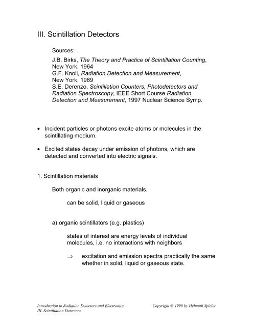
III. Scintillation Detectors
III. Scintillation Detectors
III. Scintillation Detectors

Create successful ePaper yourself
Turn your PDF publications into a flip-book with our unique Google optimized e-Paper software.
<strong>III</strong>. <strong>Scintillation</strong> <strong>Detectors</strong><br />
Sources:<br />
J.B. Birks, The Theory and Practice of <strong>Scintillation</strong> Counting,<br />
New York, 1964<br />
G.F. Knoll, Radiation Detection and Measurement,<br />
New York, 1989<br />
S.E. Derenzo, <strong>Scintillation</strong> Counters, Photodetectors and<br />
Radiation Spectroscopy, IEEE Short Course Radiation<br />
Detection and Measurement, 1997 Nuclear Science Symp.<br />
• Incident particles or photons excite atoms or molecules in the<br />
scintillating medium.<br />
• Excited states decay under emission of photons, which are<br />
detected and converted into electric signals.<br />
1. <strong>Scintillation</strong> materials<br />
Both organic and inorganic materials,<br />
can be solid, liquid or gaseous<br />
a) organic scintillators (e.g. plastics)<br />
states of interest are energy levels of individual<br />
molecules, i.e. no interactions with neighbors<br />
⇒ excitation and emission spectra practically the same<br />
whether in solid, liquid or gaseous state.<br />
Introduction to Radiation <strong>Detectors</strong> and Electronics Copyright © 1998 by Helmuth Spieler<br />
<strong>III</strong>. <strong>Scintillation</strong> <strong>Detectors</strong>
Typical energy levels<br />
(from Birks, as redrawn by Derenzo)<br />
a) At room temperature practically all electrons in ground state.<br />
(since energy of S1 states >> 0.025 eV)<br />
b) Incident radiation populates S1 states<br />
vibrational levels within S1 band decay radiation-less to<br />
S1 base state, which in turn decays under emission of<br />
light to the S0 band.<br />
c) S1 can also decay to adjacent triplet levels.<br />
Since their energy is significantly lower, the decay time is much<br />
longer.<br />
Introduction to Radiation <strong>Detectors</strong> and Electronics Copyright © 1998 by Helmuth Spieler<br />
<strong>III</strong>. <strong>Scintillation</strong> <strong>Detectors</strong>
Why isn’t emitted light re-absorbed?<br />
Since excitation goes to higher vibrational states in the S1<br />
band, whereas decay goes from the base S1 state, the<br />
emission spectrum is shifted to lower energies (longer<br />
wavelengths).<br />
⇒ only small overlap of emission and absorption spectra<br />
Introduction to Radiation <strong>Detectors</strong> and Electronics Copyright © 1998 by Helmuth Spieler<br />
<strong>III</strong>. <strong>Scintillation</strong> <strong>Detectors</strong>
Time dependence of emitted light<br />
a) non-radiative transfer of energy from vibrational states to<br />
fluorescent state<br />
typical time: 0.2 – 0.4 ns<br />
b) decay of fluorescent state<br />
typical time: 1 – 3 ns<br />
⇒ rise with time constant τr<br />
fall with time constant τf<br />
total pulse shape<br />
I t e t r<br />
( ) ∝ − − τ<br />
1<br />
− / τ<br />
I t e t f ( ) ∝<br />
f r<br />
I( t) = I ( e − e )<br />
Rise time usually increased substantially by subsequent<br />
components in system and variations in path length in large<br />
scintillators.<br />
Introduction to Radiation <strong>Detectors</strong> and Electronics Copyright © 1998 by Helmuth Spieler<br />
<strong>III</strong>. <strong>Scintillation</strong> <strong>Detectors</strong><br />
0<br />
/<br />
−t / τ −t<br />
/ τ
Properties of some typical organic scintillators<br />
Material State λmax [nm] τf [ns] ρ [g/cm 3 ] photons/MeV<br />
Anthracene crystal 447 30 1.25 1.6 . 10 4<br />
Pilot U plastic 391 1.4 1.03 1.0 . 10 4<br />
NE104 plastic 406 1.8 1.03 1.0 . 10 4<br />
NE102 liquid 425 2.6 1.51 1.2 . 10 4<br />
Introduction to Radiation <strong>Detectors</strong> and Electronics Copyright © 1998 by Helmuth Spieler<br />
<strong>III</strong>. <strong>Scintillation</strong> <strong>Detectors</strong>
Both the light output and the decay time of organic<br />
scintillators depend on the ionization density.<br />
Decay time in stilbene for various particles<br />
(from Bollinger and Thomas)<br />
Introduction to Radiation <strong>Detectors</strong> and Electronics Copyright © 1998 by Helmuth Spieler<br />
<strong>III</strong>. <strong>Scintillation</strong> <strong>Detectors</strong>
Light yield vs. ionization density<br />
(Craun and Smith)<br />
(Blanc et al.)<br />
Introduction to Radiation <strong>Detectors</strong> and Electronics Copyright © 1998 by Helmuth Spieler<br />
<strong>III</strong>. <strong>Scintillation</strong> <strong>Detectors</strong>
Variation of specific fluorescence dL/dx in anthracene with<br />
specific energy loss dE/dx (Brooks, from Birks)<br />
Introduction to Radiation <strong>Detectors</strong> and Electronics Copyright © 1998 by Helmuth Spieler<br />
<strong>III</strong>. <strong>Scintillation</strong> <strong>Detectors</strong>
Birk’s Rule<br />
For an ideal scintillator and low ionization density<br />
Luminescence ∝ Energy dissipated in scintillator<br />
or, in differential form<br />
dL<br />
dr<br />
L = SE<br />
=<br />
S dE<br />
dr<br />
The specific density of ionized and excited molecules along the<br />
particle track is<br />
B dE<br />
dr<br />
Assume that a portion of the primary excitation is lost at high<br />
ionization density (ionization quenching) and introduce a quenching<br />
parameter k. Then<br />
dL<br />
dr<br />
=<br />
1+<br />
S dE<br />
dr<br />
kB dE<br />
dr<br />
For small dE/dr this yields the luminescence yield postulated above.<br />
For large dE/dr the specific luminescence saturates, as indicated by<br />
the data.<br />
dL<br />
dr<br />
S<br />
kB const<br />
= =<br />
Introduction to Radiation <strong>Detectors</strong> and Electronics Copyright © 1998 by Helmuth Spieler<br />
<strong>III</strong>. <strong>Scintillation</strong> <strong>Detectors</strong>
The dependence of decay time on ionization density<br />
can be used for particle identification.<br />
For example, by utilizing a pulse shaping network that makes the<br />
timing of the output pulse dependent on decay time, the particle<br />
distribution is transformed into a time distribution that can be<br />
digitized directly.<br />
Example: n-γ discrimination<br />
P. Sperr, H. Spieler, M.R. Maier, NIM 116(1974)55<br />
Introduction to Radiation <strong>Detectors</strong> and Electronics Copyright © 1998 by Helmuth Spieler<br />
<strong>III</strong>. <strong>Scintillation</strong> <strong>Detectors</strong>
Inorganic Scintillators<br />
Band structure in inorganic crystals<br />
If forbidden band >> kT, no electrons in conduction band.<br />
⇒ Insulator<br />
Radiation excites electron from valence into conduction band, forming<br />
an electron-hole pair.<br />
Electrons in conduction band and holes in valence band can move<br />
freely throughout crystal.<br />
Introduction to Radiation <strong>Detectors</strong> and Electronics Copyright © 1998 by Helmuth Spieler<br />
<strong>III</strong>. <strong>Scintillation</strong> <strong>Detectors</strong>
For light emission, one must introduce states into the forbidden band,<br />
so that<br />
Three mechanisms:<br />
Examples:<br />
Eemission < Eg<br />
a) excitons (bound electron-hole pair)<br />
b) defects<br />
(interstitial atoms, for example induced by heat treatment)<br />
c) activators<br />
(from Derenzo)<br />
cooled NaI: h + + e- → exciton → phonons + photon<br />
NaI(Tl): h + + Tl + → Tl2+ e - + Tl 2+ → (Tl + )*<br />
e - + Tl + → Tl 0<br />
h + + Tl 0 → (Tl + )*<br />
(Tl + )* → Tl + + phonons + photon<br />
Introduction to Radiation <strong>Detectors</strong> and Electronics Copyright © 1998 by Helmuth Spieler<br />
<strong>III</strong>. <strong>Scintillation</strong> <strong>Detectors</strong>
Luminescence vs Quenching<br />
Excitation: A → C (very fast)<br />
thermal equilibration: C → B (~10 5 longer)<br />
Photon emission: B → D<br />
thermal equilibration: D → A<br />
(from Birks)<br />
If excited electron reaches F (depending on population of states in<br />
minimum B), the transition<br />
F → F1<br />
can proceed by phonon emission (lattice vibrations),<br />
i.e. without emission of a photon (quenching)<br />
In some crystals, the proximity region F-F1 is very close to the<br />
minimum of the excited state. These crystals are heavily quenched.<br />
Introduction to Radiation <strong>Detectors</strong> and Electronics Copyright © 1998 by Helmuth Spieler<br />
<strong>III</strong>. <strong>Scintillation</strong> <strong>Detectors</strong>
Overlap of absorption and emission spectra<br />
(from Birks)<br />
Width of absorption and emission spectra depend on population of<br />
states in the respective minima A and B.<br />
A and B must be sufficiently separated to yield adequate Stokes shift.<br />
At high temperatures the absorption and emission bands broaden,<br />
increasing the overlap and the fraction of luminescence photons lost<br />
to self-absorption.<br />
Introduction to Radiation <strong>Detectors</strong> and Electronics Copyright © 1998 by Helmuth Spieler<br />
<strong>III</strong>. <strong>Scintillation</strong> <strong>Detectors</strong>
Summary of practical inorganic scintillator materials<br />
(from Derenzo)<br />
λmax τf ρ Photons<br />
Material Form (nm) (ns) (g/cm 3 ) per MeV<br />
NaI(Tl) (20°C) crystal 415 230 3.67 38,000<br />
pure NaI (-196°C) crystal 303 60 3.67 76,000<br />
Bi4Ge3O12 (20°C) crystal 480 300 7.13 8,200<br />
Bi4Ge3O12 (-100°C) crystal 480 2000 7.13 24,000<br />
CsI(Na) crystal 420 630 4.51 39,000<br />
CsI(Tl) crystal 540 800 4.51 60,000<br />
CsI (pure) crystal 315 16 4.51 2,300<br />
CsF crystal 390 2 4.64 2,500<br />
BaF2 (slow) crystal 310 630 4.9 10,000<br />
BaF2 (fast) crystal 220 0.8 4.9 1,800<br />
Gd2SiO5(Ce) crystal 440 60 6.71 10,000<br />
CdWO4 crystal 530 15000 7.9 7,000<br />
CaWO4 crystal 430 6000 6.1 6,000<br />
CeF3 crystal 340 27 6.16 4,400<br />
PbWO4 crystal 460 2, 10, 38 8.2 500<br />
Lu2SiO5(Ce) crystal 420 40 7.4 30,000<br />
YAIO3(Ce) crystal 390 31 5.35 19,700<br />
Y2SiO5(Ce) crystal 420 70 2.70 45,000<br />
Note the wide range of decay times τf , from 0.8 ns in BaF2 to 15 μs<br />
in CdWO4.<br />
Some materials also show multiple emissions (BaF2, PbWO4).<br />
Introduction to Radiation <strong>Detectors</strong> and Electronics Copyright © 1998 by Helmuth Spieler<br />
<strong>III</strong>. <strong>Scintillation</strong> <strong>Detectors</strong>
Scintillators with Tl, Bi, etc. decay slowly due to “forbidden” transitions<br />
to the ground state:<br />
(from Derenzo)<br />
Introduction to Radiation <strong>Detectors</strong> and Electronics Copyright © 1998 by Helmuth Spieler<br />
<strong>III</strong>. <strong>Scintillation</strong> <strong>Detectors</strong>
The very fast transitions in BaF2 and CsF are due to an intermediate<br />
transition between the valence and core bands.<br />
Evv < Eg<br />
Evv > Eg<br />
fast fluorescence<br />
emission of Auger electron<br />
(energy released in the transition from the<br />
valence to the core band does not go into<br />
photon emission, but into emission of an electron<br />
to the conduction band)<br />
Competition between photon emission and Auger effect narrows the<br />
range of scintillators with fast decays:<br />
If Evv is low: longer wavelength emission, longer decay time<br />
If Evv is high: Auger emission, no scintillation light<br />
Introduction to Radiation <strong>Detectors</strong> and Electronics Copyright © 1998 by Helmuth Spieler<br />
<strong>III</strong>. <strong>Scintillation</strong> <strong>Detectors</strong>
Conversion of <strong>Scintillation</strong> Light to Electrical Signal<br />
Most Common Device:<br />
Photomultiplier Tube<br />
(from Photomultiplier Tubes, Philips Photonics)<br />
Introduction to Radiation <strong>Detectors</strong> and Electronics Copyright © 1998 by Helmuth Spieler<br />
<strong>III</strong>. <strong>Scintillation</strong> <strong>Detectors</strong>
Photocathodes<br />
Band structure in “standard” photocathode<br />
Band structure in “negative electron affinity” photocathode<br />
(from Photomultiplier Handbook, Burle Industries)<br />
Introduction to Radiation <strong>Detectors</strong> and Electronics Copyright © 1998 by Helmuth Spieler<br />
<strong>III</strong>. <strong>Scintillation</strong> <strong>Detectors</strong>
Summary of Photocathode Materials<br />
(from Derenzo)<br />
Cathode type Composition Peak Q.E. Peak λ<br />
S1 AgOCs 0.4% 800 nm<br />
S10 BiAgOCs 7% 420 nm<br />
S11 CS3SbO 21% 390 nm<br />
S20 (multi-alkali) Na2KSbCs 22% 380 nm<br />
Bialkali K2CsSb 27% 380 nm<br />
Bialkali (high temp) Na2KSb 21% 360nm<br />
KCsRbSb 24% 440 nm<br />
Bialkali RbCsSb 25% 450 nm<br />
Solar blind* CeTe 18% 200 nm<br />
Solar blind** CsI 15% 135nm<br />
* Q.E. > 0.1% above 320 nm<br />
** Q.E. > 0.1% above 210 nm<br />
Maximum quantum efficiency n above table is 27%.<br />
Is this reasonable?<br />
• no electric field within photocathode to direct electrons to<br />
emitting surface<br />
• photoelectrons initially emitted isotropically<br />
⇒ ½ directed toward faceplate<br />
⇒ ½ directed toward dynode structure<br />
• transmission losses (bialkali photocathodes 40%<br />
transmissive<br />
Introduction to Radiation <strong>Detectors</strong> and Electronics Copyright © 1998 by Helmuth Spieler<br />
<strong>III</strong>. <strong>Scintillation</strong> <strong>Detectors</strong>
(from Photomultiplier Handbook, Burle Industries)<br />
Introduction to Radiation <strong>Detectors</strong> and Electronics Copyright © 1998 by Helmuth Spieler<br />
<strong>III</strong>. <strong>Scintillation</strong> <strong>Detectors</strong>
Secondary Emission in Dynodes<br />
(D. Persyk)<br />
Introduction to Radiation <strong>Detectors</strong> and Electronics Copyright © 1998 by Helmuth Spieler<br />
<strong>III</strong>. <strong>Scintillation</strong> <strong>Detectors</strong>
Desirable to obtain high secondary emission yields to reduce<br />
fluctuations (spectral broadening).<br />
Typical dynode materials: Be0(Cs), Cs3Sb, MgO<br />
Negative electron affinity materials can also be used in dynodes<br />
(e.g. GaP(Cs), bottom distributions) – but more difficult to fabricate.<br />
(from Knoll)<br />
Introduction to Radiation <strong>Detectors</strong> and Electronics Copyright © 1998 by Helmuth Spieler<br />
<strong>III</strong>. <strong>Scintillation</strong> <strong>Detectors</strong>
High emission dynodes allow resolution of single<br />
photoelectrons<br />
(from Knoll)<br />
Introduction to Radiation <strong>Detectors</strong> and Electronics Copyright © 1998 by Helmuth Spieler<br />
<strong>III</strong>. <strong>Scintillation</strong> <strong>Detectors</strong>
Many different dynode configurations have been developed to reduce<br />
size or improve gain, uniformity over large photocathode diameters,<br />
transit time and transit time spread.<br />
(from Photomultiplier Handbook, Burle Industries)<br />
Introduction to Radiation <strong>Detectors</strong> and Electronics Copyright © 1998 by Helmuth Spieler<br />
<strong>III</strong>. <strong>Scintillation</strong> <strong>Detectors</strong>
Continuous multiplier structures<br />
Channel electron multiplier<br />
Can be combined in “microchannel plates”<br />
(from Derenzo)<br />
(from Derenzo)<br />
Introduction to Radiation <strong>Detectors</strong> and Electronics Copyright © 1998 by Helmuth Spieler<br />
<strong>III</strong>. <strong>Scintillation</strong> <strong>Detectors</strong>
Microchannel plates can be utilized in photomultipliers for ultra-fast<br />
timing with low time-dispersion.<br />
(from Photomultiplier Tubes, Philips Photonics)<br />
Introduction to Radiation <strong>Detectors</strong> and Electronics Copyright © 1998 by Helmuth Spieler<br />
<strong>III</strong>. <strong>Scintillation</strong> <strong>Detectors</strong>
Signal Evolution<br />
1. energy is absorbed in scintillator<br />
2. population of states that emit photons<br />
number of radiative states<br />
N0= Eabs /εi<br />
Eabs energy absorbed in scintillator<br />
energy required to produce 1 photon<br />
εi<br />
3. population of radiative states decays<br />
⇒ rate of photon emission<br />
dN<br />
dt<br />
ph<br />
N0 ≡ n ph(<br />
t)<br />
= e−<br />
τ<br />
Total number of photons emitted after time T<br />
4. photons absorbed in photocathode,<br />
producing photoelectrons<br />
5. photoelectrons transported through gain structure<br />
(dynodes in PMT) multiplied by G<br />
⇒ electric current at anode<br />
T<br />
∫<br />
Introduction to Radiation <strong>Detectors</strong> and Electronics Copyright © 1998 by Helmuth Spieler<br />
<strong>III</strong>. <strong>Scintillation</strong> <strong>Detectors</strong><br />
t / τ<br />
N ( T) = n ( t) dt = N ( − e )<br />
ph ph<br />
0<br />
0 1<br />
−T<br />
/ τ<br />
n ( t) = QE ⋅ n ( t) = QE ⋅ N e<br />
pe ph<br />
I ( t) = G ⋅ QE ⋅ N e<br />
anode<br />
0<br />
0<br />
−t<br />
/ τ<br />
−t<br />
/ τ
How much of this signal is actually obtained?<br />
1. Scintillator is coupled to PMT at one surface<br />
<strong>Scintillation</strong> light is emitted isotropically.<br />
(from Photomultiplier Handbook, Burle Industries)<br />
Depending on the geometry, at least half of emitted photons<br />
must be reflected one or more times to reach the faceplate of<br />
the photodetector.<br />
Light losses due to<br />
a) absorption in crystal<br />
b) reflection losses<br />
Introduction to Radiation <strong>Detectors</strong> and Electronics Copyright © 1998 by Helmuth Spieler<br />
<strong>III</strong>. <strong>Scintillation</strong> <strong>Detectors</strong>
<strong>Scintillation</strong> crystals invariably optically denser than air<br />
examples: NaI(Tl) n= 1.85<br />
CsI(Tl) n= 1.795<br />
CdWO4 n= 2.2 – 2.3<br />
BGO n= 2.152<br />
NE102 n= 1.581 (plastic)<br />
NE213 n= 1.508 (org. liquid)<br />
air n= 1<br />
⇒ Requirement for total reflection<br />
sinα ≥ 1<br />
n xtal<br />
Light incident within an angle α from normal incidence<br />
will leave the crystal.<br />
example nxtal = 1.5 ⇒ α= 42°<br />
External reflective layers can improve this situation<br />
(see following discussion of light-guides).<br />
2. Upon reaching the faceplate, light can be either transmitted<br />
or reflected<br />
refractive index of faceplate<br />
(borosilicate glass or fused silica) nfp ≈ 1.5<br />
Important to avoid air-gap<br />
(use optical grease to provide index match)<br />
Introduction to Radiation <strong>Detectors</strong> and Electronics Copyright © 1998 by Helmuth Spieler<br />
<strong>III</strong>. <strong>Scintillation</strong> <strong>Detectors</strong>
3. photons must be transmitted through the faceplate<br />
(from Photomultiplier Tubes, Philips Photonics)<br />
4. Photons must be absorbed in the photocathode<br />
(from Photomultiplier Tubes, Philips Photonics )<br />
Introduction to Radiation <strong>Detectors</strong> and Electronics Copyright © 1998 by Helmuth Spieler<br />
<strong>III</strong>. <strong>Scintillation</strong> <strong>Detectors</strong>
5. Photoelectrons must traverse the photocathode and reach<br />
the first dynode to be multiplied.<br />
It is important that the emission spectrum of the scintillator, the<br />
transmission through the faceplate and the absorption in the<br />
photocathode are matched.<br />
(from Knoll)<br />
Note that for short wavelength scintillators (for example the<br />
fast component of BaF2 at 220 nm) conventional borosilicate<br />
faceplates are very inefficient – use fused silica for extended<br />
UV response.<br />
Introduction to Radiation <strong>Detectors</strong> and Electronics Copyright © 1998 by Helmuth Spieler<br />
<strong>III</strong>. <strong>Scintillation</strong> <strong>Detectors</strong>
Typical NaI(Tl) system (from Derenzo)<br />
511 keV gamma ray<br />
⇓<br />
25000 photons in scintillator<br />
⇓<br />
15000 photons at photocathode<br />
⇓<br />
3000 photoelectrons at first dynode<br />
⇓<br />
3 . 10 9 electrons at anode<br />
2 mA peak current<br />
Resolution of energy measurement determined by statistical<br />
variance of produced signal quanta.<br />
Resolution determined by smallest number of quanta in<br />
chain, i.e. number of photoelectrons arriving at first dynode.<br />
In this example<br />
ΔE<br />
E<br />
ΔE ΔN<br />
N<br />
= = =<br />
E N N N<br />
1<br />
1<br />
= =<br />
3000<br />
2% r.m.s. = 5% FWHM<br />
Typically 7 – 8% obtained, due to non-uniformity of light<br />
collection and gain.<br />
Introduction to Radiation <strong>Detectors</strong> and Electronics Copyright © 1998 by Helmuth Spieler<br />
<strong>III</strong>. <strong>Scintillation</strong> <strong>Detectors</strong>
The PMT is often coupled to the scintillator through a<br />
light guide<br />
Match geometry of scintillator to photodetector.<br />
Spatial separation of scintillator and detector<br />
(from Knoll)<br />
Introduction to Radiation <strong>Detectors</strong> and Electronics Copyright © 1998 by Helmuth Spieler<br />
<strong>III</strong>. <strong>Scintillation</strong> <strong>Detectors</strong>
Light Transmission Through Light Guides<br />
In coupling a scintillator to a photodetector through a light guide, it is<br />
tempting to couple a large area crystal to a small area detector. This<br />
could save money and also, when using photodiodes, reduce the<br />
electronic noise.<br />
What is the efficiency of light transmission?<br />
The efficiency of light transmission through a light guide is limited by<br />
• the angle of total reflection<br />
• conservation of phase space (Liouville’s theorem)<br />
SCINTILLATOR<br />
LIGHT GUIDE<br />
PHOTODETECTOR<br />
Θ<br />
α<br />
1<br />
ϕ<br />
Δx<br />
Δx 2<br />
Introduction to Radiation <strong>Detectors</strong> and Electronics Copyright © 1998 by Helmuth Spieler<br />
<strong>III</strong>. <strong>Scintillation</strong> <strong>Detectors</strong><br />
1<br />
α 2
1. Total reflection.<br />
For rays to be reflected from the surface of the light guide the incident<br />
angle<br />
sin Θ<br />
where n is the refractive index of the light guide and next that of the<br />
external medium. When the external medium is air (next= 1)<br />
If the light guide is tapered with an angle ϕ, a ray at the limit of total<br />
reflection will impinge on the output face at an angle<br />
This is the maximum angle at the light guide output. Since the<br />
maximum reflection angle in the light guide is π / 2, the minimum<br />
angle of reflected rays at the exit is ϕ, whereas direct rays can<br />
impinge with zero angle.<br />
≥<br />
sin Θ ≥<br />
π<br />
2<br />
next n<br />
2. Conservation of phase space<br />
(see D. Marcuse, BSTJ 45 (1966) 743, Applied Optics 10/3 (1971) 494)<br />
The trajectories of photons can be described analogously to particles<br />
whose position and slope are described as a point in phase space<br />
with the coordinates x and p. For photons these canonically<br />
conjugate variables are the the transverse coordinates of the photon<br />
ray and its angle. In two dimensions (adopted here for simplicity) the<br />
variables are the transverse coordinate x and the quantity<br />
p = n sinα<br />
where n is the refractive index of the medium and α is the angular<br />
divergence of the photon beam.<br />
Introduction to Radiation <strong>Detectors</strong> and Electronics Copyright © 1998 by Helmuth Spieler<br />
<strong>III</strong>. <strong>Scintillation</strong> <strong>Detectors</strong><br />
1<br />
n<br />
+ ϕ − Θ
At the entrance of the light guide the transverse dimension is Δx1, so<br />
if the maximum angle of a light ray is α1, the volume element in<br />
phase space is<br />
Correspondingly, at the output<br />
Since the volume element must be conserved<br />
a maximum acceptance angle α2 at the output means that at the<br />
input only rays within an entry angle<br />
can propagate through the light guide.<br />
• Note that even if total reflection obtained over all angles (n= ∞),<br />
a light guide with Δx1 >> Δx2 would incur substantial light loss<br />
because of limitation of the acceptance angle.<br />
As shown above, total internal reflection allows a maximum angle of<br />
so<br />
Δx<br />
Δp<br />
= 2Δx nsinα<br />
1<br />
2<br />
1<br />
Δx<br />
Δp<br />
= 2Δx n sinα<br />
1<br />
2<br />
Δx<br />
Δp<br />
= Δx<br />
Δp<br />
1<br />
Δx<br />
2 sinα1 = sinα<br />
2<br />
Δx1<br />
α<br />
2<br />
1<br />
Introduction to Radiation <strong>Detectors</strong> and Electronics Copyright © 1998 by Helmuth Spieler<br />
<strong>III</strong>. <strong>Scintillation</strong> <strong>Detectors</strong><br />
2<br />
2<br />
2<br />
,<br />
1<br />
π<br />
= + ϕ − Θ<br />
2<br />
⎛π<br />
⎞<br />
2<br />
sinα<br />
2 =<br />
sin⎜<br />
+ ϕ − Θ⎟<br />
= cos( Θ −ϕ<br />
) = 1−<br />
sin ( Θ − ϕ)<br />
⎝ 2 ⎠<br />
2
For simplification, assume that the lightguide is only slightly tapered<br />
(ϕ
Implementation of Light Guides<br />
ref: Kilvington et al., NIM 80 (1970) 177<br />
Experimental arrangement<br />
Where the condition for total reflection<br />
is not met, an external reflector can<br />
help.<br />
Introduction to Radiation <strong>Detectors</strong> and Electronics Copyright © 1998 by Helmuth Spieler<br />
<strong>III</strong>. <strong>Scintillation</strong> <strong>Detectors</strong>
Variation of pulse height with length of light guide<br />
a) Total internal reflection only<br />
b) Total internal reflection with reflective coating<br />
either... aluminum foil<br />
aluminized mylar<br />
transparent mylar painted with<br />
reflective paint<br />
c) Surface of light guide coated with reflective paint<br />
d) Specular reflector without light guide<br />
e) Diffuse reflector without light guide<br />
Although peak light output can be improved by reflective<br />
coatings, this only obtains with short light guides.<br />
Critical that surface of light guide be smooth.<br />
Introduction to Radiation <strong>Detectors</strong> and Electronics Copyright © 1998 by Helmuth Spieler<br />
<strong>III</strong>. <strong>Scintillation</strong> <strong>Detectors</strong>
Operational aspects of using PMTs<br />
Electron multiplication at dynodes depends on potential<br />
between successive dynodes.<br />
Potential distribution commonly set by resistive divider.<br />
(from Photomultiplier Tubes, Philips Photonics )<br />
Secondary electrons are emitted with low energy and<br />
accelerated by potential difference between dynodes.<br />
Secondary emission coefficients of commonly used dynode<br />
materials vs. incident electron energy:<br />
Introduction to Radiation <strong>Detectors</strong> and Electronics Copyright © 1998 by Helmuth Spieler<br />
<strong>III</strong>. <strong>Scintillation</strong> <strong>Detectors</strong>
The gain of GaP(Cs) NEA dynodes does not exhibit the gain<br />
saturation of conventional materials.<br />
(from Photomultiplier Tubes, Philips Photonics )<br />
Advantageous especially at first dynode to improve gain<br />
distribution of multiplication chain.<br />
Typically, PMTs are operated with total supply voltages of<br />
2 kV.<br />
8 to 14 stages (number of dynodes) are common,<br />
with 100 to 150 V between dynodes.<br />
The potential between the photocathode and the<br />
first dynode is typically 4 times as large to improve the<br />
collection efficiency and the gain in the first stage.<br />
Introduction to Radiation <strong>Detectors</strong> and Electronics Copyright © 1998 by Helmuth Spieler<br />
<strong>III</strong>. <strong>Scintillation</strong> <strong>Detectors</strong>
Peak currents of anode pulses can be as high as 20 mA.<br />
If the voltage divider is not capable of providing this current,<br />
the acceleration potential will “sag”, leading to non-linearity.<br />
(Note that total gain changes with n-th power of voltage!)<br />
Necessary to provide capacitors as “charge reservoirs”:<br />
(from Burle Photomultiplier Handbook)<br />
DC current through resistive divider must be much greater<br />
(>10x, preferably more) than the average signal current.<br />
The average current at a gamma rate of n s -1 is<br />
= n ⋅ N el,<br />
anode<br />
I ⋅ q<br />
Using the NaI(Tl) example used before, for which each<br />
511 keV gamma produced 3 . 10 9 electrons at the anode,<br />
the average signal current at a rate of 10 5 s -1 is 48 μA.<br />
Thus, the standing current in the resistive divider should be<br />
1 mA or more, leading to a power (heat) dissipation of 2 W at<br />
2 kV total supply voltage.<br />
Introduction to Radiation <strong>Detectors</strong> and Electronics Copyright © 1998 by Helmuth Spieler<br />
<strong>III</strong>. <strong>Scintillation</strong> <strong>Detectors</strong><br />
e
Scintillators with higher light output or running at higher rates<br />
might require 10 mA, which becomes thermally problematic.<br />
In these cases, voltage dividers transistor current buffers are<br />
often used.<br />
(from Burle Photomultiplier Handbook)<br />
Although the polarity of the supply voltage is fixed, i.e. the<br />
anode must be more positive than the cathode, one can<br />
choose whether the anode or cathode is at ground potential.<br />
Although grounding the cathode is widespread, oparation<br />
with the anode at ground potential is advantageous in<br />
systems operating with fast output pulses and high counting<br />
rates. The only drawback is that the photocathode end of the<br />
tube must be well-insulated from ground to prevent corona<br />
discarge near the photocathode.<br />
The voltage distribution in the dynode chain can be<br />
optimized for<br />
• high gain<br />
• time resolution<br />
• good linearity up to high peak currents<br />
Recommended voltage distributions can be found in the<br />
manufacturers data sheets.<br />
Introduction to Radiation <strong>Detectors</strong> and Electronics Copyright © 1998 by Helmuth Spieler<br />
<strong>III</strong>. <strong>Scintillation</strong> <strong>Detectors</strong>
Connections to the anode and adjacent dynodes must be<br />
made with low inductance to avoid parasitic resonances.<br />
Upper waveform: correct pulse<br />
Lower waveform: superimposed “ringing” due to parasitic<br />
resonances<br />
(from Burle Photomultiplier Handbook)<br />
Introduction to Radiation <strong>Detectors</strong> and Electronics Copyright © 1998 by Helmuth Spieler<br />
<strong>III</strong>. <strong>Scintillation</strong> <strong>Detectors</strong>
Photomultiplier tubes are sensitive to magnetic fields<br />
(from Burle Photomultiplier Handbook)<br />
Even in a laboratory environment, PMTs must be<br />
surrounded by magnetic shielding (“mu metal”) to avoid<br />
orientation-dependent gain changes due to stray magnetic<br />
fields.<br />
Typical: 25% decrease in gain at 0.1 mT<br />
Conventional PMTs will not function inside the magnet of a<br />
tracking detector!<br />
Alternatives: MCP PMTs<br />
Semiconductor photodiodes<br />
special dynode structures<br />
Introduction to Radiation <strong>Detectors</strong> and Electronics Copyright © 1998 by Helmuth Spieler<br />
<strong>III</strong>. <strong>Scintillation</strong> <strong>Detectors</strong>
Time Response of Photomultiplier Tubes<br />
For a typical fast 2” PMT (Philips XP2020) the transit time from the<br />
photocathode to the anode is about 30 ns at 2000V.<br />
The intrinsic rise time is 1.6 ns, due to broadening of the initial<br />
electron packet in the course of the multiplication process.<br />
The transit time varies by 0.25 ns between the center of the<br />
photocathode and a radius of 18 mm.<br />
For two tubes operating in coincidence at a signal level of 1500<br />
photoelectrons, a time resolution of 230 ps is possible.<br />
Special dynode structures are used to reduce transit time spread.<br />
Example: time compensating structure<br />
(from Burle Photomultiplier Handbook)<br />
Introduction to Radiation <strong>Detectors</strong> and Electronics Copyright © 1998 by Helmuth Spieler<br />
<strong>III</strong>. <strong>Scintillation</strong> <strong>Detectors</strong>
Various Dynode Structures<br />
(from “Photomultiplier Tubes”, Philips Photonics )<br />
a) Venetian blind<br />
Allows simple input system with high collection efficiency.<br />
Good gain stability, but mediocre timing performance<br />
b) Box and Grid: characteristics similar to a)<br />
c) Linear focusing: good timing characteristics<br />
d) Circular cage: compact<br />
e) Mesh dynodes: low gain, but usable up to B= 1 T<br />
f) Foil dynodes: perforated metal foils – particularly<br />
useful for multi-channel anodes<br />
Introduction to Radiation <strong>Detectors</strong> and Electronics Copyright © 1998 by Helmuth Spieler<br />
<strong>III</strong>. <strong>Scintillation</strong> <strong>Detectors</strong>