DDR SO-DIMM Specification - Discobolus Designs, Home Page
DDR SO-DIMM Specification - Discobolus Designs, Home Page
DDR SO-DIMM Specification - Discobolus Designs, Home Page

You also want an ePaper? Increase the reach of your titles
YUMPU automatically turns print PDFs into web optimized ePapers that Google loves.
JEDEC Standard No. 21-C<br />
<strong>Page</strong> 4.20.6-1<br />
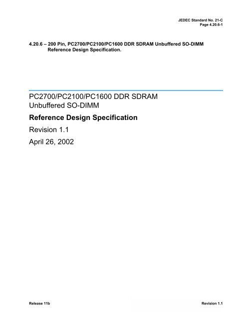
4.20.6 – 200 Pin, PC2700/PC2100/PC1600 <strong>DDR</strong> SDRAM Unbuffered <strong>SO</strong>-<strong>DIMM</strong><br />
Reference Design <strong>Specification</strong>.<br />
PC2700/PC2100/PC1600 <strong>DDR</strong> SDRAM<br />
Unbuffered <strong>SO</strong>-<strong>DIMM</strong><br />
Reference Design <strong>Specification</strong><br />
Revision 1.1<br />
April 26, 2002<br />
Release 11b Revision 1.1
JEDEC Standard No. 21-C<br />
<strong>Page</strong> 4.20.6-2<br />
Contents<br />
1. Product Description ........................................................................................................................... 3<br />
Product Family Attributes ................................................................................................................... 3<br />
2. Environmental Requirements ............................................................................................................ 4<br />
Absolute Maximum Ratings ............................................................................................................... 4<br />
3. Architecture ......................................................................................................................................... 4<br />
Pin Description ................................................................................................................................... 4<br />
Input/Output Functional Description ................................................................................................... 5<br />
<strong>DDR</strong> SDRAM <strong>SO</strong>-<strong>DIMM</strong> Pinout ......................................................................................................... 6<br />
Block Diagram: Raw Card Version C, x64 variant (one physical bank of x16 SDRAMs).................... 7<br />
Block Diagram: Raw Card Version A (two physical banks of x16 SDRAMs) ...................................... 8<br />
Block Diagram: Raw Card Version B (one physical bank of x8 SDRAMs) ......................................... 9<br />
Block Diagram: Raw Card Version C, x72 variant (one physical bank of x16 SDRAMs plus<br />
one x16 SDRAM)....................................................................................................... 10<br />
Logical Clock Net Structures............................................................................................................... 11<br />
Clock Net Wiring (4 loads) ................................................................................................................. 11<br />
4. Component Details.............................................................................................................................. 12<br />
Pin Assignments for 64 Mb and 128 Mb 66 pin <strong>DDR</strong> SDRAM Planar Components .......................... 12<br />
Pin Assignments for 256 Mb and 512 Mb 66 pin <strong>DDR</strong> SDRAM Planar Components ........................ 13<br />
Reference <strong>DDR</strong> SDRAM Component <strong>Specification</strong>s ......................................................................... 14<br />
Reference SPD Component <strong>Specification</strong>s ....................................................................................... 14<br />
5. Unbuffered <strong>SO</strong>-<strong>DIMM</strong> Details ............................................................................................................. 15<br />
<strong>DDR</strong> SDRAM Module Configurations (Reference <strong>Designs</strong>) ............................................................... 15<br />
PC2100 Gerber File Releases ........................................................................................................... 15<br />
Example Raw Card Component Placement ....................................................................................... 16<br />
6. <strong>SO</strong>-<strong>DIMM</strong> Wiring Details ..................................................................................................................... 17<br />
Signal Groups .................................................................................................................................... 17<br />
General Net Structure Routing Guidelines ......................................................................................... 17<br />
Explanation of Net Structure Diagrams .............................................................................................. 17<br />
Data Net Structures ............................................................................................................................ 18<br />
Select Net Structures ......................................................................................................................... 19<br />
Clock Enable Net Structures .............................................................................................................. 20<br />
Address/Control Net Structures ......................................................................................................... 21<br />
Cross Section Recommendations ...................................................................................................... 22<br />
7. Serial Presence Detect Definition ..................................................................................................... 23<br />
8. Product Label....................................................................................................................................... 26<br />
9. <strong>DDR</strong> <strong>SO</strong>-<strong>DIMM</strong> Mechanical <strong>Specification</strong>s ........................................................................................27<br />
Revision 1.1<br />
Release 11b
JEDEC Standard No. 21-C<br />
<strong>Page</strong> 4.20.6-3<br />
1. Product Description<br />
This reference specification defines the electrical and mechanical requirements for the PC2700 module, a<br />
200-pin, 167 MHz clock (333 MT/s data rate), 64-bit wide, Unbuffered Synchronous Double Data Rate (<strong>DDR</strong>)<br />
DRAM Small Outline Dual In-Line Memory Module (<strong>DDR</strong> SDRAM <strong>SO</strong>-<strong>DIMM</strong>s). It also defines a slower version,<br />
PC2100, using 133 MHz clock (266 MT/s data rate) or PC1600, using 100 MHz clock (200 MT/s data<br />
rate) <strong>DDR</strong> SDRAMs. These <strong>DDR</strong> SDRAM <strong>SO</strong>-<strong>DIMM</strong>s are intended for use as main memory when installed in<br />
systems such as mobile personal computers.<br />
Reference design examples are included which provide an initial basis for Unbuffered <strong>SO</strong>-<strong>DIMM</strong> designs.<br />
Any modifications to these reference designs must meet all system timing, signal integrity and thermal<br />
requirements for the supported maximum clock rate. Other designs are acceptable, and all Unbuffered <strong>SO</strong>-<br />
<strong>DIMM</strong> implementations must use simulations and lab verification to ensure proper timing requirements and<br />
signal integrity in the design.<br />
Product Family Attributes<br />
Attribute: Values: Notes:<br />
<strong>SO</strong>-<strong>DIMM</strong> Organization x 64, x 72<br />
<strong>SO</strong>-<strong>DIMM</strong> Dimensions (nominal)<br />
<strong>SO</strong>-<strong>DIMM</strong> Types Supported<br />
31.75 mm high, 67.60 mm wide<br />
Unbuffered, Unbuffered with PLL, Registered with PLL<br />
Pin Count 200<br />
SDRAMs Supported<br />
Capacity<br />
64 Mb, 128 Mb, 256 Mb, 512 Mb<br />
32 MB, 64 MB, 128 MB, 256 MB, 512 MB<br />
Serial Presence Detect Consistent with JEDEC Rev. 1.0<br />
Voltage Options<br />
Interface<br />
2.5 V V DD<br />
2.5 V V DD Q<br />
2.5 V to 3.3 V V DD SPD 1<br />
SSTL_2<br />
Note 1: V DD SPD is not tied to V DD or V DD Q on the <strong>DDR</strong> <strong>SO</strong>-<strong>DIMM</strong>.<br />
Release 11b Revision 1.1
JEDEC Standard No. 21-C<br />
<strong>Page</strong> 4.20.6-4<br />
2. Environmental Requirements<br />
PC2700 <strong>DDR</strong> SDRAM Unbuffered <strong>SO</strong>-<strong>DIMM</strong>s are intended for use in mobile computing environments that<br />
have limited capacity for heat dissipation.<br />
Absolute Maximum Ratings<br />
Symbol Parameter Rating Units Notes<br />
T OPR Operating Temperature (ambient) 0 to +65 °C 1<br />
H OPR Operating Humidity (relative) 10 to 90 % 1<br />
T STG Storage Temperature -50 to +100 °C 1<br />
H STG Storage Humidity (without condensation) 5 to 95 % 1<br />
Barometric Pressure (operating & storage) 105 to 69 kPa 1, 2<br />
1. Stresses greater than those listed may cause permanent damage to the device. This is a stress rating only, and device functional<br />
operation at or above the conditions indicated is not implied. Exposure to absolute maximum rating conditions for extended periods<br />
may affect reliability.<br />
2. Up to 9850 ft.<br />
3. Architecture<br />
Pin Description<br />
CK(0:2) Clock Inputs, positive line 3 DQ(0:63) Data Input/Output 64<br />
CK(0:2) Clock inputs, negative line 3 CB(7:0) Data check bits Input/Output 8<br />
CKE(0:1) Clock Enables 2 DM(0:8) Data Masks 9<br />
RAS Row Address Strobe 1 DQS(0:8) Data strobes 9<br />
CAS Column Address Strobe 1<br />
WE Write Enable 1<br />
S(0:1) Chip Selects 2 V DD Core and I/O Power 33<br />
A(0:9,11:12) Address Inputs 12 V SS Ground 33<br />
A10/AP Address Input/Autoprecharge 1 V REF Input/Output Reference 2<br />
BA(0:1) SDRAM Bank Address 2 V DD SPD SPD Power 1<br />
SCL<br />
Serial Presence Detect (SPD)<br />
Clock Input<br />
1 V DD ID V DD , V DD Q level detection 1<br />
SDA SPD Data Input/Output 1<br />
SA(0:2) SPD address 3 DU Reserved for future use 7<br />
Total: 200<br />
Revision 1.1<br />
Release 11b
JEDEC Standard No. 21-C<br />
<strong>Page</strong> 4.20.6-5<br />
Input/Output Functional Description<br />
Symbol Type Polarity Function<br />
CK0 - CK2,<br />
CK0 - CK2<br />
Input<br />
Cross<br />
point<br />
The system clock inputs. All address and command lines are sampled on the cross point of the<br />
rising edge of CK and falling edge of CK. A Delay Locked Loop (DLL) circuit is driven from the<br />
clock inputs and output timing for read operations is synchronized to the input clock.<br />
CKE0, CKE1 Input Active High<br />
S0, S1 Input Active Low<br />
Activates the <strong>DDR</strong> SDRAM CK signal when high and deactivates the CK signal when low. By<br />
deactivating the clocks, CKE low initiates the Power Down mode or the Self Refresh mode.<br />
Enables the associated <strong>DDR</strong> SDRAM command decoder when low and disables the command<br />
decoder when high. When the command decoder is disabled, new commands are ignored but<br />
previous operations continue. Physical Bank 0 is selected by S0; Bank 1 is selected by S1.<br />
RAS, CAS,<br />
WE<br />
Input Active Low<br />
When sampled at the cross point of the rising edge of CK and falling edge of CK, CAS, RAS,<br />
and WE define the operation to be executed by the SDRAM.<br />
BA0 - BA1 Input — Selects which <strong>DDR</strong> SDRAM bank of four is activated.<br />
A0 - A9,<br />
A11-A12<br />
A10/AP<br />
Input —<br />
During a Bank Activate command cycle, defines the row address when sampled at the cross<br />
point of the rising edge of CK and falling edge of CK. During a Read or Write command cycle,<br />
defines the column address when sampled at the cross point of the rising edge of CK and falling<br />
edge of CK. In addition to the column address, AP is used to invoke autoprecharge operation<br />
at the end of the burst read or write cycle. If AP is high, autoprecharge is selected and<br />
BA0, BA1 defines the bank to be precharged. If AP is low, autoprecharge is disabled. During a<br />
Precharge command cycle, AP is used in conjunction with BA0, BA1 to control which bank(s)<br />
to precharge. If AP is high, all banks will be precharged regardless of the state of BA0 or BA1.<br />
If AP is low, then BA0 and BA1 are used to define which bank to precharge.<br />
DQ0 - DQ63 In/Out — Data Bit Input/Output pins.<br />
CB0 - CB7 In/Out — Data Check Bit Input/Output pins. Not used on x64 modules.<br />
DM0 - DM8 Input Active High<br />
DQS0 - DQS8 In/Out —<br />
The data write masks, associated with one data byte. In Write mode, DM operates as a byte<br />
mask by allowing input data to be written if it is low but blocks the write operation if it is high. In<br />
Read mode, DM lines have no effect. DM8 is associated with check bits CB0-CB7, and is not<br />
used on x64 modules.<br />
The data strobes, associated with one data byte, sourced with data transfers. In Write mode,<br />
the data strobe is sourced by the controller and is centered in the data window. In Read mode,<br />
the data strobe is sourced by the <strong>DDR</strong> SDRAMs and is sent at the leading edge of the data<br />
window. DQS8 is associated with check bits CB0-CB7, and is not used on x64 modules.<br />
V DD , V DD SPD,<br />
V SS<br />
Supply — Power supplies for core, I/O, Serial Presence Detect, and ground for the module.<br />
V DD ID Out —<br />
SDA In/Out —<br />
SCL Input —<br />
Defines relationship of V DD and V DD Q. If V DD ID is open, V DD = V DD Q; if V DD ID is pulled to<br />
V SS , V DD ≠ V DD Q. This line should be pulled high through 10 KΩ on the host board.<br />
This is a bidirectional pin used to transfer data into or out of the SPD EEPROM. A resistor must<br />
be connected to V DD to act as a pull up.<br />
This signal is used to clock data into and out of the SPD EEPROM. A resistor may be connected<br />
from SCL to V DD to act as a pull up.<br />
SA0 - SA2 Input — Address pins used to select the Serial Presence Detect.<br />
Release 11b Revision 1.1
JEDEC Standard No. 21-C<br />
<strong>Page</strong> 4.20.6-6<br />
.<br />
<strong>DDR</strong> SDRAM <strong>SO</strong>-<strong>DIMM</strong> Pinout<br />
Pin Front<br />
# Side<br />
Pin Back<br />
# Side<br />
Pin Front<br />
# Side<br />
Pin Back<br />
# Side<br />
Pin Front<br />
# Side<br />
Pin Back<br />
# Side<br />
Pin Front<br />
# Side<br />
Pin Back<br />
# Side<br />
1 V REF 2 V REF 51 V SS 52 V SS 101 A9 102 A8 151 DQ42 152 DQ46<br />
3 V SS 4 V SS 53 DQ19 54 DQ23 103 V SS 104 V SS 153 DQ43 154 DQ47<br />
5 DQ0 6 DQ4 55 DQ24 56 DQ28 105 A7 106 A6 155 V DD 156 V DD<br />
7 DQ1 8 DQ5 57 V DD 58 V DD 107 A5 108 A4 157 V DD 158 CK1<br />
9 V DD 10 V DD 59 DQ25 60 DQ29 109 A3 110 A2 159 V SS 160 CK1<br />
11 DQS0 12 DM0 61 DQS3 62 DM3 111 A1 112 A0 161 V SS 162 V SS<br />
13 DQ2 14 DQ6 63 V SS 64 V SS 113 V DD 114 V DD 163 DQ48 164 DQ52<br />
15 V SS 16 V SS 65 DQ26 66 DQ30 115 A10/AP 116 BA1 165 DQ49 166 DQ53<br />
17 DQ3 18 DQ7 67 DQ27 68 DQ31 117 BA0 118 RAS 167 V DD 168 V DD<br />
19 DQ8 20 DQ12 69 V DD 70 V DD 119 WE 120 CAS 169 DQS6 170 DM6<br />
21 V DD 22 V DD 71 CB0 72 CB4 121 S0 122 S1 171 DQ50 172 DQ54<br />
23 DQ9 24 DQ13 73 CB1 74 CB5 123<br />
DU<br />
(A13)<br />
124 DU 173 V SS 174 V SS<br />
25 DQS1 26 DM1 75 V SS 76 V SS 125 V SS 126 V SS 175 DQ51 176 DQ55<br />
27 V SS 28 V SS 77 DQS8 78 DM8 127 DQ32 128 DQ36 177 DQ56 178 DQ60<br />
29 DQ10 30 DQ14 79 CB2 80 CB6 129 DQ33 130 DQ37 179 V DD 180 V DD<br />
31 DQ11 32 DQ15 81 V DD 82 V DD 131 V DD 132 V DD 181 DQ57 182 DQ61<br />
33 V DD 34 V DD 83 CB3 84 CB7 133 DQS4 134 DM4 183 DQS7 184 DM7<br />
35 CK0 36 V DD 85 DU 86<br />
DU<br />
(RESET)<br />
135 DQ34 136 DQ38 185 V SS 186 V SS<br />
37 CK0 38 V SS 87 V SS 88 V SS 137 V SS 138 V SS 187 DQ58 188 DQ62<br />
39 V SS 40 V SS 89 CK2 90 V SS 139 DQ35 140 DQ39 189 DQ59 190 DQ63<br />
41 DQ16 42 DQ20 91 CK2 92 V DD 141 DQ40 142 DQ44 191 V DD 192 V DD<br />
43 DQ17 44 DQ21 93 V DD 94 V DD 143 V DD 144 V DD 193 SDA 194 SA0<br />
45 V DD 46 V DD 95 CKE1 96 CKE0 145 DQ41 146 DQ45 195 SCL 196 SA1<br />
47 DQS2 48 DM2 97 DU 98 DU 147 DQS5 148 DM5 197 V DD SPD 198 SA2<br />
49 DQ18 50 DQ22 99 A12 100 A11 149 V SS 150 V SS 199 V DD ID 200 DU<br />
Note: Pins 71, 72, 73, 74, 77, 78, 79, 80, 83, 84 are reserved for x72 variants of this module and are not used on the x64 versions.<br />
Note: Pin 86 is reserved for a registered variant of this module and is not used on the unbuffered version.<br />
Note: Pins 89, 91are reserved for x72 modules or registered modules.<br />
Note: Pin 123 reserved for higher density memories, requiring A13<br />
Revision 1.1<br />
Release 11b
JEDEC Standard No. 21-C<br />
<strong>Page</strong> 4.20.6-7<br />
Block Diagram: Raw Card Version C (Populated as 1 physical bank of x16 SDRAMs)<br />
DQS0<br />
DM0<br />
DQS1<br />
DM1<br />
S0<br />
DQ0<br />
DQ1<br />
DQ2<br />
DQ3<br />
DQ4<br />
DQ5<br />
DQ6<br />
DQ7<br />
DQ8<br />
DQ9<br />
DQ10<br />
DQ11<br />
DQ12<br />
DQ13<br />
DQ14<br />
DQ15<br />
LDQS<br />
LDM<br />
I/O 0<br />
I/O 1<br />
I/O 2<br />
I/O 3<br />
I/O 4<br />
I/O 5<br />
I/O 6<br />
I/O 7<br />
UDQS<br />
UDM<br />
I/O 8<br />
I/O 9<br />
I/O 10<br />
I/O 11<br />
I/O 12<br />
I/O 13<br />
I/O 14<br />
I/O 15<br />
S<br />
D0<br />
DQS4<br />
DM4<br />
DQS5<br />
DM5<br />
DQ32<br />
DQ33<br />
DQ34<br />
DQ35<br />
DQ36<br />
DQ37<br />
DQ38<br />
DQ39<br />
DQ40<br />
DQ41<br />
DQ42<br />
DQ43<br />
DQ44<br />
DQ45<br />
DQ46<br />
DQ47<br />
LDQS<br />
LDM<br />
I/O 0<br />
I/O 1<br />
I/O 2<br />
I/O 3<br />
I/O 4<br />
I/O 5<br />
I/O 6<br />
I/O 7<br />
UDQS<br />
UDM<br />
I/O 8<br />
I/O 9<br />
I/O 10<br />
I/O 11<br />
I/O 12<br />
I/O 13<br />
I/O 14<br />
I/O 15<br />
S<br />
D2<br />
DQS2<br />
DM2<br />
DQS3<br />
DM3<br />
DQ16<br />
DQ17<br />
DQ18<br />
DQ19<br />
DQ20<br />
DQ21<br />
DQ22<br />
DQ23<br />
DQ24<br />
DQ25<br />
DQ26<br />
DQ27<br />
DQ28<br />
DQ29<br />
DQ30<br />
DQ31<br />
LDQS<br />
LDM<br />
I/O 0<br />
I/O 1<br />
I/O 2<br />
I/O 3<br />
I/O 4<br />
I/O 5<br />
I/O 6<br />
I/O 7<br />
UDQS<br />
UDM<br />
I/O 8<br />
I/O 9<br />
I/O 10<br />
I/O 11<br />
I/O 12<br />
I/O 13<br />
I/O 14<br />
I/O 15<br />
S<br />
D1<br />
DQS6<br />
DM6<br />
DQS7<br />
DM7<br />
DQ48<br />
DQ49<br />
DQ50<br />
DQ51<br />
DQ52<br />
DQ53<br />
DQ54<br />
DQ55<br />
DQ56<br />
DQ57<br />
DQ58<br />
DQ59<br />
DQ60<br />
DQ61<br />
DQ62<br />
DQ63<br />
LDQS<br />
LDM<br />
I/O 0<br />
I/O 1<br />
I/O 2<br />
I/O 3<br />
I/O 4<br />
I/O 5<br />
I/O 6<br />
I/O 7<br />
UDQS<br />
UDM<br />
I/O 8<br />
I/O 9<br />
I/O 10<br />
I/O 11<br />
I/O 12<br />
I/O 13<br />
I/O 14<br />
I/O 15<br />
S<br />
D3<br />
SCL<br />
SA0<br />
SA1<br />
SA2<br />
Serial Presence Detect (SPD)<br />
A0<br />
SDA<br />
A1<br />
A2<br />
WP<br />
BA0-BA1<br />
A0-AN<br />
RAS<br />
CAS<br />
WE<br />
CKE0<br />
CKE1<br />
V DD SPD<br />
V REF<br />
V DD<br />
V SS<br />
V DD ID<br />
#Unless otherwise noted, resistor values are 22 Ω ± 5%<br />
SDRAMS D0-D3<br />
SDRAMS D0-D3<br />
SDRAMS D0-D3<br />
SDRAMS D0-D3<br />
SDRAMS D0-D3<br />
SDRAMS D0-D3<br />
N.C.<br />
SPD<br />
SDRAMS D0-D3<br />
SDRAMS D0-D3 V DD and V DD Q<br />
SDRAMS D0-D3, SPD<br />
CK0<br />
CK0<br />
CK1<br />
CK1<br />
CK2<br />
CK2<br />
2 loads<br />
2 loads<br />
0 loads<br />
Note: DQ wiring may differ from that described<br />
in this drawing; however DQ/DM/DQS<br />
relationships are maintained as shown.<br />
V DD ID strap connections:<br />
(for memory device V DD , V DD Q)<br />
Strap out (open): V DD = V DD Q<br />
Strap in (closed): V DD ≠ V DD Q<br />
Release 11b Revision 1.1
JEDEC Standard No. 21-C<br />
<strong>Page</strong> 4.20.6-8<br />
Block Diagram: Raw Card Version A (Populated as 2 physical banks of x16 SDRAMs)<br />
DQS0<br />
DM0<br />
DQS1<br />
DM1<br />
S1<br />
S0<br />
DQ0<br />
DQ1<br />
DQ2<br />
DQ3<br />
DQ4<br />
DQ5<br />
DQ6<br />
DQ7<br />
DQ8<br />
DQ9<br />
DQ10<br />
DQ11<br />
DQ12<br />
DQ13<br />
DQ14<br />
DQ15<br />
S<br />
LDQS<br />
LDM<br />
I/O 0<br />
I/O 1<br />
I/O 2<br />
I/O 3<br />
I/O 4<br />
I/O 5<br />
I/O 6<br />
I/O 7<br />
UDM<br />
I/O 8<br />
I/O 9<br />
I/O 10<br />
I/O 11<br />
I/O 12<br />
I/O 13<br />
I/O 14<br />
I/O 15<br />
D0<br />
S<br />
LDQS<br />
LDM<br />
I/O 0<br />
I/O 1<br />
I/O 2<br />
I/O 3<br />
I/O 4<br />
I/O 5<br />
I/O 6<br />
I/O 7<br />
UDM<br />
I/O 8<br />
I/O 9<br />
I/O 10<br />
I/O 11<br />
I/O 12<br />
I/O 13<br />
I/O 14<br />
I/O 15<br />
D4<br />
DQS4<br />
DM4<br />
DQS5<br />
DM5<br />
DQ32<br />
DQ33<br />
DQ34<br />
DQ35<br />
DQ36<br />
DQ37<br />
DQ38<br />
DQ39<br />
DQ40<br />
DQ41<br />
DQ42<br />
DQ43<br />
DQ44<br />
DQ45<br />
DQ46<br />
DQ47<br />
S<br />
LDQS<br />
LDM<br />
I/O 0<br />
I/O 1<br />
I/O 2<br />
I/O 3<br />
I/O 4<br />
I/O 5<br />
I/O 6<br />
I/O 7<br />
UDQS<br />
UDM<br />
I/O 8<br />
I/O 9<br />
I/O 10<br />
I/O 11<br />
I/O 12<br />
I/O 13<br />
I/O 14<br />
I/O 15<br />
D2<br />
S<br />
LDQS<br />
LDM<br />
I/O 0<br />
I/O 1<br />
I/O 2<br />
I/O 3<br />
I/O 4<br />
I/O 5<br />
I/O 6<br />
I/O 7<br />
UDQS UDQS UDQS<br />
UDM<br />
I/O 8<br />
I/O 9<br />
I/O 10<br />
I/O 11<br />
I/O 12<br />
I/O 13<br />
I/O 14<br />
I/O 15<br />
D6<br />
DQS2<br />
DM2<br />
DQS3<br />
DM3<br />
DQ16<br />
DQ17<br />
DQ18<br />
DQ19<br />
DQ20<br />
DQ21<br />
DQ22<br />
DQ23<br />
DQ24<br />
DQ25<br />
DQ26<br />
DQ27<br />
DQ28<br />
DQ29<br />
DQ30<br />
DQ31<br />
S<br />
LDQS<br />
LDM<br />
I/O 0<br />
I/O 1<br />
I/O 2<br />
I/O 3<br />
I/O 4<br />
I/O 5<br />
I/O 6<br />
I/O 7<br />
UDQS<br />
UDM<br />
I/O 8<br />
I/O 9<br />
I/O 10<br />
I/O 11<br />
I/O 12<br />
I/O 13<br />
I/O 14<br />
I/O 15<br />
D1<br />
S<br />
LDQS<br />
LDM<br />
I/O 0<br />
I/O 1<br />
I/O 2<br />
I/O 3<br />
I/O 4<br />
I/O 5<br />
I/O 6<br />
I/O 7<br />
UDQS<br />
UDM<br />
I/O 8<br />
I/O 9<br />
I/O 10<br />
I/O 11<br />
I/O 12<br />
I/O 13<br />
I/O 14<br />
I/O 15<br />
D5<br />
DQS6<br />
DM6<br />
DQS7<br />
DM7<br />
DQ48<br />
DQ49<br />
DQ50<br />
DQ51<br />
DQ52<br />
DQ53<br />
DQ54<br />
DQ55<br />
DQ56<br />
DQ57<br />
DQ58<br />
DQ59<br />
DQ60<br />
DQ61<br />
DQ62<br />
DQ63<br />
S<br />
LDQS<br />
LDM<br />
I/O 0<br />
I/O 1<br />
I/O 2<br />
I/O 3<br />
I/O 4<br />
I/O 5<br />
I/O 6<br />
I/O 7<br />
UDQS<br />
UDM<br />
I/O 8<br />
I/O 9<br />
I/O 10<br />
I/O 11<br />
I/O 12<br />
I/O 13<br />
I/O 14<br />
I/O 15<br />
D3<br />
S<br />
LDQS<br />
LDM<br />
I/O 0<br />
I/O 1<br />
I/O 2<br />
I/O 3<br />
I/O 4<br />
I/O 5<br />
I/O 6<br />
I/O 7<br />
UDQS<br />
UDM<br />
I/O 8<br />
I/O 9<br />
I/O 10<br />
I/O 11<br />
I/O 12<br />
I/O 13<br />
I/O 14<br />
I/O 15<br />
D7<br />
SCL<br />
SA0<br />
SA1<br />
SA2<br />
Serial Presence Detect (SPD)<br />
A0<br />
SDA<br />
A1<br />
A2<br />
WP<br />
BA0-BA1<br />
A0-AN<br />
RAS<br />
CAS<br />
WE<br />
CKE0<br />
CKE1<br />
#Unless otherwise noted, resistor values are 22 Ω ± 5%<br />
SDRAMS D0-D7<br />
SDRAMS D0-D7<br />
SDRAMS D0-D7<br />
SDRAMS D0-D7<br />
SDRAMS D0-D7<br />
SDRAMS D0-D3<br />
SDRAMS D4-D7<br />
CK0<br />
CK0<br />
CK1<br />
CK1<br />
CK2<br />
CK2<br />
4 loads<br />
4 loads<br />
0 loads<br />
V DD SPD<br />
V REF<br />
V DD<br />
V SS<br />
V DD ID<br />
SPD<br />
SDRAMS D0-D7<br />
SDRAMS D0-D7 V DD and V DD Q<br />
SDRAMS D0-D7, SPD<br />
Note: DQ wiring may differ from that described<br />
in this drawing; however DQ/DM/DQS<br />
relationships are maintained as shown.<br />
V DD ID strap connections:<br />
(for memory device V DD , V DD Q)<br />
Strap out (open): V DD = V DD Q<br />
Strap in (closed): V DD ≠ V DD Q<br />
Revision 1.1<br />
Release 11b
JEDEC Standard No. 21-C<br />
<strong>Page</strong> 4.20.6-9<br />
Block Diagram: Raw Card Version B (Populated as 1 physical bank of x8 SDRAMs)<br />
DQS0<br />
DM0<br />
DQS1<br />
DM1<br />
S0<br />
DQ0<br />
DQ1<br />
DQ2<br />
DQ3<br />
DQ4<br />
DQ5<br />
DQ6<br />
DQ7<br />
DQ8<br />
DQ9<br />
DQ10<br />
DQ11<br />
DQ12<br />
DQ13<br />
DQ14<br />
DQ15<br />
DQS<br />
DM<br />
I/O 0<br />
I/O 1<br />
I/O 2<br />
I/O 3<br />
I/O 4<br />
I/O 5<br />
I/O 6<br />
I/O 7<br />
DQS<br />
DM<br />
I/O 0<br />
I/O 1<br />
I/O 2<br />
I/O 3<br />
I/O 4<br />
I/O 5<br />
I/O 6<br />
I/O 7<br />
S<br />
D0<br />
S<br />
D1<br />
DQS4<br />
DM4<br />
DQS5<br />
DM5<br />
DQ32<br />
DQ33<br />
DQ34<br />
DQ35<br />
DQ36<br />
DQ37<br />
DQ38<br />
DQ39<br />
DQ40<br />
DQ41<br />
DQ42<br />
DQ43<br />
DQ44<br />
DQ45<br />
DQ46<br />
DQ47<br />
DQS<br />
DM<br />
I/O 0<br />
I/O 1<br />
I/O 2<br />
I/O 3<br />
I/O 4<br />
I/O 5<br />
I/O 6<br />
I/O 7<br />
DQS<br />
DM<br />
I/O 0<br />
I/O 1<br />
I/O 2<br />
I/O 3<br />
I/O 4<br />
I/O 5<br />
I/O 6<br />
I/O 7<br />
S<br />
D4<br />
S<br />
D5<br />
DQS2<br />
DM2<br />
DQS3<br />
DM3<br />
DQ16<br />
DQ17<br />
DQ18<br />
DQ19<br />
DQ20<br />
DQ21<br />
DQ22<br />
DQ23<br />
DQ24<br />
DQ25<br />
DQ26<br />
DQ27<br />
DQ28<br />
DQ29<br />
DQ30<br />
DQ31<br />
DQS<br />
DM<br />
I/O 0<br />
I/O 1<br />
I/O 2<br />
I/O 3<br />
I/O 4<br />
I/O 5<br />
I/O 6<br />
I/O 7<br />
DQS<br />
DM<br />
I/O 0<br />
I/O 1<br />
I/O 2<br />
I/O 3<br />
I/O 4<br />
I/O 5<br />
I/O 6<br />
I/O 7<br />
S<br />
D2<br />
S<br />
D3<br />
DQS6<br />
DM6<br />
DQS7<br />
DM7<br />
DQ48<br />
DQ49<br />
DQ50<br />
DQ51<br />
DQ52<br />
DQ53<br />
DQ54<br />
DQ55<br />
DQ56<br />
DQ57<br />
DQ58<br />
DQ59<br />
DQ60<br />
DQ61<br />
DQ62<br />
DQ63<br />
DQS<br />
DM<br />
I/O 0<br />
I/O 1<br />
I/O 2<br />
I/O 3<br />
I/O 4<br />
I/O 5<br />
I/O 6<br />
I/O 7<br />
DQS<br />
DM<br />
I/O 0<br />
I/O 1<br />
I/O 2<br />
I/O 3<br />
I/O 4<br />
I/O 5<br />
I/O 6<br />
I/O 7<br />
S<br />
D6<br />
S<br />
D7<br />
SCL<br />
SA0<br />
SA1<br />
SA2<br />
Serial Presence Detect (SPD)<br />
A0<br />
SDA<br />
A1<br />
A2<br />
WP<br />
BA0-BA1<br />
A0-AN<br />
RAS<br />
CAS<br />
WE<br />
CKE0<br />
CKE1<br />
#Unless otherwise noted, resistor values are 22 Ω ± 5%<br />
SDRAMS D0-D7<br />
SDRAMS D0-D7<br />
SDRAMS D0-D7<br />
SDRAMS D0-D7<br />
SDRAMS D0-D7<br />
SDRAMS D0-D7<br />
N.C.<br />
CK0<br />
CK0<br />
CK1<br />
CK1<br />
CK2<br />
CK2<br />
4 loads<br />
4 loads<br />
0 loads<br />
V DD SPD<br />
V REF<br />
V DD<br />
V SS<br />
V DD ID<br />
SPD<br />
SDRAMS D0-D7<br />
SDRAMS D0-D7 V DD and V DD Q<br />
SDRAMS D0-D7, SPD<br />
Note: DQ wiring may differ from that described<br />
in this drawing; however DQ/DM/DQS<br />
relationships are maintained as shown.<br />
V DD ID strap connections:<br />
(for memory device V DD , V DD Q)<br />
Strap out (open): V DD = V DD Q<br />
Strap in (closed): V DD ≠ V DD Q<br />
Release 11b Revision 1.1
JEDEC Standard No. 21-C<br />
<strong>Page</strong> 4.20.6-10<br />
Block Diagram: Raw Card Version C (Populated as 1 physical bank of x16 SDRAMs and 1 x16 SDRAM)<br />
DQS0<br />
DM0<br />
DQS1<br />
DM1<br />
S0<br />
DQ0<br />
DQ1<br />
DQ2<br />
DQ3<br />
DQ4<br />
DQ5<br />
DQ6<br />
DQ7<br />
DQ8<br />
DQ9<br />
DQ10<br />
DQ11<br />
DQ12<br />
DQ13<br />
DQ14<br />
DQ15<br />
LDQS<br />
LDM<br />
I/O 0<br />
I/O 1<br />
I/O 2<br />
I/O 3<br />
I/O 4<br />
I/O 5<br />
I/O 6<br />
I/O 7<br />
UDQS<br />
UDM<br />
I/O 8<br />
I/O 9<br />
I/O 10<br />
I/O 11<br />
I/O 12<br />
I/O 13<br />
I/O 14<br />
I/O 15<br />
S<br />
D0<br />
DQS4<br />
DM4<br />
DQS5<br />
DM5<br />
DQ32<br />
DQ33<br />
DQ34<br />
DQ35<br />
DQ36<br />
DQ37<br />
DQ38<br />
DQ39<br />
DQ40<br />
DQ41<br />
DQ42<br />
DQ43<br />
DQ44<br />
DQ45<br />
DQ46<br />
DQ47<br />
LDQS<br />
LDM<br />
I/O 0<br />
I/O 1<br />
I/O 2<br />
I/O 3<br />
I/O 4<br />
I/O 5<br />
I/O 6<br />
I/O 7<br />
UDQS<br />
UDM<br />
I/O 8<br />
I/O 9<br />
I/O 10<br />
I/O 11<br />
I/O 12<br />
I/O 13<br />
I/O 14<br />
I/O 15<br />
S<br />
D2<br />
DQS8<br />
DM8<br />
CB0<br />
CB1<br />
CB2<br />
CB3<br />
CB4<br />
CB5<br />
CB6<br />
CB7<br />
V DD Q<br />
22<br />
DQS<br />
DM<br />
I/O 0<br />
I/O 1<br />
I/O 2<br />
I/O 3<br />
I/O 4<br />
I/O 5<br />
I/O 6<br />
I/O 7<br />
47K<br />
UDQS<br />
UDM<br />
I/O 8<br />
I/O 9<br />
I/O 10<br />
I/O 11<br />
I/O 12<br />
I/O 13<br />
I/O 14<br />
I/O 15<br />
S<br />
D4<br />
DQS2<br />
DM2<br />
DQS3<br />
DM3<br />
DQ16<br />
DQ17<br />
DQ18<br />
DQ19<br />
DQ20<br />
DQ21<br />
DQ22<br />
DQ23<br />
DQ24<br />
DQ25<br />
DQ26<br />
DQ27<br />
DQ28<br />
DQ29<br />
DQ30<br />
DQ31<br />
LDQS<br />
LDM<br />
I/O 0<br />
I/O 1<br />
I/O 2<br />
I/O 3<br />
I/O 4<br />
I/O 5<br />
I/O 6<br />
I/O 7<br />
UDQS<br />
UDM<br />
I/O 8<br />
I/O 9<br />
I/O 10<br />
I/O 11<br />
I/O 12<br />
I/O 13<br />
I/O 14<br />
I/O 15<br />
S<br />
D1<br />
DQS6<br />
DM6<br />
DQS7<br />
DM7<br />
DQ48<br />
DQ49<br />
DQ50<br />
DQ51<br />
DQ52<br />
DQ53<br />
DQ54<br />
DQ55<br />
DQ56<br />
DQ57<br />
DQ58<br />
DQ59<br />
DQ60<br />
DQ61<br />
DQ62<br />
DQ63<br />
LDQS<br />
LDM<br />
I/O 0<br />
I/O 1<br />
I/O 2<br />
I/O 3<br />
I/O 4<br />
I/O 5<br />
I/O 6<br />
I/O 7<br />
UDQS<br />
UDM<br />
I/O 8<br />
I/O 9<br />
I/O 10<br />
I/O 11<br />
I/O 12<br />
I/O 13<br />
I/O 14<br />
I/O 15<br />
S<br />
D3<br />
SCL<br />
SA0<br />
SA1<br />
SA2<br />
Serial Presence Detect (SPD)<br />
A0<br />
SDA<br />
A1<br />
A2<br />
WP<br />
BA0-BA1<br />
A0-AN<br />
RAS<br />
CAS<br />
WE<br />
CKE0<br />
CKE1<br />
#Unless otherwise noted, resistor values are 22 Ω ± 5%<br />
SDRAMS D0-D4<br />
SDRAMS D0-D4<br />
SDRAMS D0-D4<br />
SDRAMS D0-D4<br />
SDRAMS D0-D4<br />
SDRAMS D0-D4<br />
N.C.<br />
CK0<br />
CK0<br />
CK1<br />
CK1<br />
CK2<br />
CK2<br />
2 loads<br />
2 loads<br />
1 load<br />
V DD SPD<br />
V REF<br />
V DD<br />
V SS<br />
V DD ID<br />
SPD<br />
SDRAMS D0-D4<br />
SDRAMS D0-D4 V DD and V DD Q<br />
SDRAMS D0-D4, SPD<br />
Note: DQ wiring may differ from that described<br />
in this drawing; however DQ/DM/DQS<br />
relationships are maintained as shown.<br />
V DD ID strap connections:<br />
(for memory device V DD , V DD Q)<br />
Strap out (open): V DD = V DD Q<br />
Strap in (closed): V DD ≠ V DD Q<br />
Revision 1.1<br />
Release 11b
JEDEC Standard No. 21-C<br />
<strong>Page</strong> 4.20.6-11<br />
Logical Clock Net Structures<br />
<strong>SO</strong>-<strong>DIMM</strong><br />
Connector<br />
CK<br />
CK<br />
Zero Loads<br />
10 pF<br />
<strong>SO</strong>-<strong>DIMM</strong><br />
Connector<br />
CK<br />
CK<br />
R = 120 Ω<br />
± 5%<br />
Two Loads<br />
DRAM1<br />
Cap<br />
DRAM3<br />
Cap<br />
R = 120 Ω<br />
± 5%<br />
CK<br />
<strong>SO</strong>-<strong>DIMM</strong><br />
CK<br />
Connector<br />
Four Loads<br />
DRAM1<br />
DRAM2<br />
DRAM3<br />
DRAM4<br />
R = 120 Ω<br />
± 5%<br />
CK<br />
<strong>SO</strong>-<strong>DIMM</strong><br />
CK<br />
Connector<br />
One Load<br />
DRAM1<br />
Cap<br />
Cap<br />
Cap<br />
R = 120 Ω<br />
± 5%<br />
CK<br />
CK<br />
<strong>SO</strong>-<strong>DIMM</strong><br />
Connector<br />
Three Loads<br />
DRAM1<br />
DRAM2<br />
DRAM3<br />
Cap<br />
CK<br />
CK<br />
Cap<br />
1.5 pF<br />
Clock Net Wiring<br />
TL2<br />
TL3<br />
SDRAM<br />
or Cap<br />
CK<br />
CK<br />
<strong>SO</strong>-<strong>DIMM</strong><br />
Connector<br />
TL0<br />
R = 120 Ω<br />
± 5%<br />
TL1<br />
TL2<br />
TL3<br />
TL3<br />
SDRAM<br />
or Cap<br />
SDRAM<br />
or Cap<br />
TL3<br />
SDRAM<br />
or Cap<br />
Clock Routing Trace Lengths:<br />
Segment TL0 TL1 TL2 TL3<br />
Raw Card Min Max Min Max Min Max Min Max<br />
A, B 0.15 0.16 0.05 0.06 0.82 0.83 0.32 0.33<br />
C 0.15 0.16 0.04 0.05 0.81 0.82 0.32 0.33<br />
Release 11b Revision 1.1
JEDEC Standard No. 21-C<br />
<strong>Page</strong> 4.20.6-12<br />
4. Component Details<br />
Pin Assignments for 64 Mb and 128 Mb <strong>DDR</strong> SDRAM Planar Components (Top View)<br />
V DD<br />
DQ0<br />
V DD Q<br />
DQ1<br />
DQ2<br />
V SS Q<br />
DQ3<br />
DQ4<br />
V DD Q<br />
DQ5<br />
DQ6<br />
V SS Q<br />
DQ7<br />
NC<br />
V DD Q<br />
LDQS<br />
NC<br />
V DD<br />
NU,QFC<br />
LDM<br />
WE<br />
CAS<br />
RAS<br />
S<br />
NC<br />
BA0<br />
BA1<br />
A10/AP<br />
A0<br />
A1<br />
A2<br />
A3<br />
V DD<br />
1<br />
2<br />
3<br />
4<br />
5<br />
6<br />
7<br />
8<br />
9<br />
10<br />
11<br />
12<br />
13<br />
14<br />
15<br />
16<br />
17<br />
18<br />
19<br />
20<br />
21<br />
22<br />
23<br />
24<br />
25<br />
26<br />
27<br />
28<br />
29<br />
30<br />
31<br />
32<br />
66<br />
65<br />
64<br />
63<br />
62<br />
61<br />
60<br />
59<br />
58<br />
57<br />
56<br />
55<br />
54<br />
53<br />
52<br />
51<br />
50<br />
49<br />
48<br />
47<br />
46<br />
45<br />
44<br />
43<br />
42<br />
41<br />
40<br />
39<br />
38<br />
37<br />
36<br />
35<br />
33 34<br />
V SS<br />
DQ15<br />
V SS Q<br />
DQ14<br />
DQ13<br />
V DD Q<br />
DQ12<br />
DQ11<br />
V SS Q<br />
DQ10<br />
DQ9<br />
V DD Q<br />
DQ8<br />
NC<br />
V SS Q<br />
UDQS<br />
NC<br />
V REF<br />
V SS<br />
UDM<br />
CK<br />
CK<br />
CKE<br />
NC<br />
NC<br />
A11<br />
A9<br />
A8<br />
A7<br />
A6<br />
A5<br />
A4<br />
V SS<br />
V DD<br />
DQ0<br />
V DD Q<br />
NC<br />
DQ1<br />
V SS Q<br />
NC<br />
DQ2<br />
V DD Q<br />
NC<br />
DQ3<br />
V SS Q<br />
NC<br />
NC<br />
V DD Q<br />
LDQS<br />
NC<br />
V DD<br />
NU,QFC<br />
LDM<br />
WE<br />
CAS<br />
RAS<br />
S<br />
NC<br />
BA0<br />
BA1<br />
A10/AP<br />
A0<br />
A1<br />
A2<br />
A3<br />
V DD<br />
1<br />
66<br />
2<br />
65<br />
3<br />
64<br />
4<br />
63<br />
5<br />
62<br />
6<br />
61<br />
7<br />
60<br />
8<br />
59<br />
9<br />
58<br />
10<br />
57<br />
11<br />
56<br />
12<br />
55<br />
13<br />
54<br />
14<br />
53<br />
15<br />
52<br />
16<br />
51<br />
17<br />
50<br />
18<br />
49<br />
19<br />
48<br />
20<br />
47<br />
21<br />
46<br />
22<br />
45<br />
23<br />
44<br />
24<br />
43<br />
25<br />
42<br />
26<br />
41<br />
27<br />
40<br />
28<br />
39<br />
29<br />
38<br />
30<br />
37<br />
31<br />
36<br />
32<br />
35<br />
33 34<br />
V SS<br />
DQ7<br />
V SS Q<br />
NC<br />
DQ6<br />
V DD Q<br />
NC<br />
DQ5<br />
V SS Q<br />
NC<br />
DQ4<br />
V DD Q<br />
NC<br />
NC<br />
V SS Q<br />
UDQS<br />
NC<br />
V REF<br />
V SS<br />
UDM<br />
CK<br />
CK<br />
CKE<br />
NC<br />
NC<br />
A11<br />
A9<br />
A8<br />
A7<br />
A6<br />
A5<br />
A4<br />
V SS<br />
66-pin Plastic<br />
T<strong>SO</strong>P(II) 400 mil<br />
1 Mbit x 16 I/O x 4 Bank<br />
2 Mbit x 16 I/O x 4 Bank<br />
66-pin Plastic<br />
T<strong>SO</strong>P(II) 400 mil<br />
2 Mbit x 8 I/O x 4 Bank<br />
4 Mbit x 8 I/O x 4 Bank<br />
Note: Raw Card Versions ‘A’ through ‘C’ support the use of the above <strong>DDR</strong> SDRAM pin assignments.<br />
These pin assignments are consistent with the JEDEC standard package definition.<br />
Revision 1.1<br />
Release 11b
JEDEC Standard No. 21-C<br />
<strong>Page</strong> 4.20.6-13<br />
Pin Assignments for 256 Mb and 512 Mb 66 pin <strong>DDR</strong> SDRAM Planar Components<br />
(Top View)<br />
V DD<br />
DQ0<br />
V DD Q<br />
DQ1<br />
DQ2<br />
V SS Q<br />
DQ3<br />
DQ4<br />
V DD Q<br />
DQ5<br />
DQ6<br />
V SS Q<br />
DQ7<br />
NC<br />
V DD Q<br />
LDQS<br />
NC<br />
V DD<br />
NU,QFC<br />
LDM<br />
WE<br />
CAS<br />
RAS<br />
S<br />
NC<br />
BA0<br />
BA1<br />
A10/AP<br />
A0<br />
A1<br />
A2<br />
A3<br />
V DD<br />
1<br />
66<br />
2<br />
65<br />
3<br />
64<br />
4<br />
63<br />
5<br />
62<br />
6<br />
61<br />
7<br />
60<br />
8<br />
59<br />
9<br />
58<br />
10<br />
57<br />
11<br />
56<br />
12<br />
55<br />
13<br />
54<br />
14<br />
53<br />
15<br />
52<br />
16<br />
51<br />
17<br />
50<br />
18<br />
49<br />
19<br />
48<br />
20<br />
47<br />
21<br />
46<br />
22<br />
45<br />
23<br />
44<br />
24<br />
43<br />
25<br />
42<br />
26<br />
41<br />
27<br />
40<br />
28<br />
39<br />
29<br />
38<br />
30<br />
37<br />
31<br />
36<br />
32<br />
35<br />
33 34<br />
V SS<br />
DQ15<br />
V SS Q<br />
DQ14<br />
DQ13<br />
V DD Q<br />
DQ12<br />
DQ11<br />
V SS Q<br />
DQ10<br />
DQ9<br />
V DD Q<br />
DQ8<br />
NC<br />
V SS Q<br />
UDQS<br />
NC<br />
V REF<br />
V SS<br />
UDM<br />
CK<br />
CK<br />
CKE<br />
NC<br />
A12<br />
A11<br />
A9<br />
A8<br />
A7<br />
A6<br />
A5<br />
A4<br />
V SS<br />
V DD<br />
DQ0<br />
V DD Q<br />
NC<br />
DQ1<br />
V SS Q<br />
NC<br />
DQ2<br />
V DD Q<br />
NC<br />
DQ3<br />
V SS Q<br />
NC<br />
NC<br />
V DD Q<br />
LDQS<br />
NC<br />
V DD<br />
NU,QFC<br />
LDM<br />
WE<br />
CAS<br />
RAS<br />
S<br />
NC<br />
BA0<br />
BA1<br />
A10/AP<br />
A0<br />
A1<br />
A2<br />
A3<br />
V DD<br />
1<br />
2<br />
3<br />
4<br />
5<br />
6<br />
7<br />
8<br />
9<br />
10<br />
11<br />
12<br />
13<br />
14<br />
15<br />
16<br />
17<br />
18<br />
19<br />
20<br />
21<br />
22<br />
23<br />
24<br />
25<br />
26<br />
27<br />
28<br />
29<br />
30<br />
31<br />
32<br />
66<br />
65<br />
64<br />
63<br />
62<br />
61<br />
60<br />
59<br />
58<br />
57<br />
56<br />
55<br />
54<br />
53<br />
52<br />
51<br />
50<br />
49<br />
48<br />
47<br />
46<br />
45<br />
44<br />
43<br />
42<br />
41<br />
40<br />
39<br />
38<br />
37<br />
36<br />
35<br />
33 34<br />
V SS<br />
DQ7<br />
V SS Q<br />
NC<br />
DQ6<br />
V DD Q<br />
NC<br />
DQ5<br />
V SS Q<br />
NC<br />
DQ4<br />
V DD Q<br />
NC<br />
NC<br />
V SS Q<br />
UDQS<br />
NC<br />
V REF<br />
V SS<br />
UDM<br />
CK<br />
CK<br />
CKE<br />
NC<br />
A12<br />
A11<br />
A9<br />
A8<br />
A7<br />
A6<br />
A5<br />
A4<br />
V SS<br />
66-pin Plastic<br />
T<strong>SO</strong>P(II) 400 mil<br />
4 Mbit x 16 I/O x 4 Bank<br />
8 Mbit x 16 I/O x 4 Bank<br />
66-pin Plastic<br />
T<strong>SO</strong>P(II) 400 mil<br />
8 Mbit x 8 I/O x 4 Bank<br />
16 Mbit x 8 I/O x 4 Bank<br />
Note: Raw Card Versions ‘A’ through ‘C’ support the use of the above <strong>DDR</strong> SDRAM pin assignments.<br />
These pin assignments are consistent with the JEDEC standard package definition.<br />
Release 11b Revision 1.1
JEDEC Standard No. 21-C<br />
<strong>Page</strong> 4.20.6-14<br />
Reference <strong>DDR</strong> SDRAM Component <strong>Specification</strong>s<br />
The <strong>DDR</strong> SDRAM components used with this <strong>SO</strong>-<strong>DIMM</strong> design specification are intended to be consistent<br />
with the latest revision of the JEDEC <strong>DDR</strong>333, <strong>DDR</strong>266 and <strong>DDR</strong>200 SDRAM specifications. Refer to standard<br />
JESD-79 for component details.<br />
Reference SPD Component <strong>Specification</strong>s<br />
The Serial Presence Detect EEPROMs have their own power pin, V DD SPD, so that they can be programmed<br />
or read without powering up the rest of the module. The wide voltage range permits use with 2.5V or 3.3V<br />
serial buses.<br />
DC Electrical Characteristics<br />
Symbol Parameter Min Max Units<br />
V DD SPD Core Supply Voltage 2.3 3.6 V<br />
Revision 1.1<br />
Release 11b
JEDEC Standard No. 21-C<br />
<strong>Page</strong> 4.20.6-15<br />
5. Unbuffered <strong>SO</strong>-<strong>DIMM</strong> Details<br />
<strong>DDR</strong> SDRAM Module Configurations (Reference <strong>Designs</strong>)<br />
Raw<br />
Card<br />
Version<br />
<strong>SO</strong>-<strong>DIMM</strong><br />
Capacity<br />
<strong>SO</strong>-<strong>DIMM</strong><br />
Organization<br />
SDRAM<br />
Density<br />
SDRAM<br />
Organization<br />
# of<br />
SDRAMs<br />
SDRAM<br />
Package Type<br />
# of<br />
Physical<br />
Banks<br />
# of Banks<br />
in SDRAM<br />
# Address bits<br />
row/col<br />
A 64 MB 8 M x 64 64 Mbit 4 M x 16 8 66 lead T<strong>SO</strong>P 2 4 12/8<br />
A 128 MB 16 M x 64 128 Mbit 8 M x 16 8 66 lead T<strong>SO</strong>P 2 4 12/9<br />
A 256 MB 32 M x 64 256 Mbit 16 M x 16 8 66 lead T<strong>SO</strong>P 2 4 13/9<br />
A 512 MB 64 M x 64 512 Mbit 32 M x 16 8 66 lead T<strong>SO</strong>P 2 4 13/10<br />
Raw<br />
Card<br />
Version<br />
<strong>SO</strong>-<strong>DIMM</strong><br />
Capacity<br />
<strong>SO</strong>-<strong>DIMM</strong><br />
Organization<br />
SDRAM<br />
Density<br />
SDRAM<br />
Organization<br />
# of<br />
SDRAMs<br />
SDRAM<br />
Package Type<br />
# of<br />
Physical<br />
Banks<br />
# of Banks<br />
in SDRAM<br />
# Address bits<br />
row/col<br />
B 64 MB 8 M x 64 64 Mbit 8 M x 8 8 66 lead T<strong>SO</strong>P 1 4 12/9<br />
B 128 MB 16 M x 64 128 Mbit 16 M x 8 8 66 lead T<strong>SO</strong>P 1 4 12/10<br />
B 256 MB 32 M x 64 256 Mbit 32 M x 8 8 66 lead T<strong>SO</strong>P 1 4 13/10<br />
B 512 MB 64 M x 64 512 Mbit 64 M x 8 8 66 lead T<strong>SO</strong>P 1 4 13/11<br />
Raw<br />
Card<br />
Version<br />
<strong>SO</strong>-<strong>DIMM</strong><br />
Capacity<br />
<strong>SO</strong>-<strong>DIMM</strong><br />
Organization<br />
SDRAM<br />
Density<br />
SDRAM<br />
Organization<br />
# of<br />
SDRAMs<br />
SDRAM<br />
Package Type<br />
# of<br />
Physical<br />
Banks<br />
# of Banks<br />
in SDRAM<br />
# Address bits<br />
row/col<br />
C 32 MB 4 M x 64 64 Mbit 4 M x 16 4 66 lead T<strong>SO</strong>P 1 4 12/8<br />
C 32 MB 4 M x 72 64 Mbit 4 M x 16 5 66 lead T<strong>SO</strong>P 1 4 12/8<br />
C 64 MB 8 M x 64 128 Mbit 8 M x 16 4 66 lead T<strong>SO</strong>P 1 4 12/9<br />
C 64 MB 8 M x 72 128 Mbit 8 M x 16 5 66 lead T<strong>SO</strong>P 1 4 12/9<br />
C 128 MB 16 M x 64 256 Mbit 16 M x 16 4 66 lead T<strong>SO</strong>P 1 4 13/9<br />
C 128 MB 16 M x 72 256 Mbit 16 M x 16 5 66 lead T<strong>SO</strong>P 1 4 13/9<br />
C 256 MB 32 M x 64 512 Mbit 32 M x 16 4 66 lead T<strong>SO</strong>P 1 4 13/10<br />
C 256 MB 32 M x 72 512 Mbit 32 M x 16 5 66 lead T<strong>SO</strong>P 1 4 13/10<br />
PC2700 Gerber Releases<br />
Reference design file updates will be released as needed. This specification will reflect the most recent<br />
design files, but may be updated to reflect clarifications to the specification only; in these cases, the design<br />
files will not be updated. The following table outlines the most recent design file releases:<br />
Raw Card<br />
Gerber<br />
Revision<br />
Applicable<br />
design file<br />
Notes<br />
A 1.0 A0 Released 6/2001<br />
B 1.0 B0 Released 6/2001<br />
C 1.0 C0 Released 6/2001<br />
Release 11b Revision 1.1
JEDEC Standard No. 21-C<br />
<strong>Page</strong> 4.20.6-16<br />
Example Raw Card Component Placement<br />
The component layout for Raw Cards A, B, and C are similar. In the case of Raw Card C, only one component<br />
will be included on the rear side of the card for ECC. This example is for reference only; please refer to<br />
JEDEC standard MO-224 variation BA for details.<br />
2.0 mm<br />
<strong>DDR</strong> SDRAMs<br />
Front View<br />
<strong>DDR</strong> SDRAMs<br />
SPD<br />
2.0 mm<br />
Component<br />
Keepout<br />
Area<br />
1 39 41<br />
199<br />
Rear View<br />
2.0 mm 2.0 mm<br />
2 40 42<br />
200<br />
R/C C:<br />
ECC<br />
<strong>DDR</strong> SDRAMs<br />
<strong>DDR</strong> SDRAMs<br />
Revision 1.1<br />
Release 11b
JEDEC Standard No. 21-C<br />
<strong>Page</strong> 4.20.6-17<br />
6. <strong>SO</strong>-<strong>DIMM</strong> Wiring Details<br />
Signal Groups<br />
This reference specification categorizes SDRAM timing-critical signals into seven groups whose members<br />
have identical loadings and routings. The following table summarizes the signals contained in each group.<br />
.<br />
Signal Group Signals In Group <strong>Page</strong><br />
Clocks for Unbuffered <strong>SO</strong>-<strong>DIMM</strong> CK [2:0], CK [2:0] 11<br />
Data, Check Bits, Data Mask, Data<br />
Strobe<br />
DQ [63:0], CB[7:0], DM[8:0], DQS[8:0] 18<br />
Select S [1:0] 19<br />
Clock Enable CKE [1:0] 20<br />
Address/Control Ax, BAx, RAS, CAS, WE 21<br />
General Net Structure Routing Guidelines<br />
Net structures and lengths must satisfy signal quality and setup/hold time requirements for the memory interface.<br />
Net structure diagrams for each signal group are shown in the following sections. Each diagram is<br />
accompanied by a trace length table that lists the minimum and maximum allowable lengths for each trace<br />
segment and/or net.<br />
The general routing recommendations are as follows. Other stackups and layouts are possible that meet the<br />
electrical characteristics.<br />
• Route all signal traces except clocks using 4 mil rules, 6 mil minimum spacing between adjacent traces.<br />
• Route clocks as much as possible using the inner layers.<br />
• Internal signal layers and the power plane should have a ground ring around the perimeter of the board,<br />
stitched to ground at 0.5" intervals. The ground ring should be at least 20 mils wide where layout permits,<br />
but can be reduced to 10 mils when necessary.<br />
• No test points are required.<br />
Explanation of Net Structure Diagrams<br />
The net structure routing diagrams provide a reference design example for each raw card version. These<br />
designs provide an initial basis for unbuffered <strong>SO</strong>-<strong>DIMM</strong> designs. The diagrams should be used to determine<br />
individual signal wiring on a <strong>SO</strong>-<strong>DIMM</strong> for any supported configuration. Only transmission lines (represented<br />
as cylinders and labeled with trace length designators “TL”) represent physical trace segments. All other lines<br />
are zero in length. To verify <strong>SO</strong>-<strong>DIMM</strong> functionality, a full simulation of all signal integrity and timing is<br />
required. The given net structures and trace lengths are not inclusive for all solutions.<br />
Once the net structure has been determined, the permitted trace lengths for the net structure can be read<br />
from the table below each net structure routing diagram. Some configurations require the use of multiple net<br />
structure routing diagrams to account for varying load quantities on the same signal. All diagrams define one<br />
load as one <strong>DDR</strong> SDRAM input. The net structure routing data in this document accurately represent reference<br />
Raw Card versions A, B and C.<br />
Release 11b Revision 1.1
JEDEC Standard No. 21-C<br />
<strong>Page</strong> 4.20.6-18<br />
Data Net Structures DQ[63:0], CB[7:0], DM[8:0], DQS[8:0]<br />
Net Structure Routing for Data, Check Bits, Data Mask, Data Strobe<br />
<strong>SO</strong>-<strong>DIMM</strong><br />
Connector<br />
TL0<br />
22 Ω ± 5%<br />
TL1<br />
TL2<br />
SDRAM Pin<br />
SDRAM Pin<br />
TL2<br />
For designs using two physical banks<br />
Trace Lengths for Data Net Structure<br />
TL0 TL1 TL2 Total<br />
Raw card Min Max Min Max Min Max Min Max<br />
A 0.15 0.16 0.64 0.75 0.11 0.20 1.00 1.07<br />
B 0.15 0.15 0.83 0.84 - - 0.99 1.00<br />
C 0.15 0.16 0.82 0.85 - - 0.98 1.00<br />
All distances are given in inches and should be kept within a tolerance of ± 0.01 inch<br />
Revision 1.1<br />
Release 11b
JEDEC Standard No. 21-C<br />
<strong>Page</strong> 4.20.6-19<br />
Select Net Structures S [1:0]<br />
Net Structure Routing for Select<br />
SDRAM Pin<br />
TL4<br />
TL4<br />
SDRAM Pin<br />
TL3<br />
SDRAM Pin<br />
TL4<br />
TL4<br />
SDRAM Pin<br />
TL2<br />
<strong>SO</strong>-<strong>DIMM</strong><br />
Connector<br />
TL0<br />
For one bank x8 only<br />
TL1<br />
SDRAM Pin<br />
TL4<br />
TL4<br />
SDRAM Pin<br />
TL3<br />
SDRAM Pin<br />
TL4<br />
TL4<br />
SDRAM Pin<br />
For x72 ECC design<br />
Trace Lengths for Select Net Structures<br />
TL0 TL1 TL2 TL3 TL4<br />
Raw Card Min Max Min Max Min Max Min Max Min Max<br />
A 4.01 4.01 0.43 0.45 0.43 0.45 0.60 0.60 0.14 0.20<br />
B 1.36 1.38 0.34 0.35 0.34 0.35 0.61 0.61 0.27 0.27<br />
C 3.48 3.49 0.39 0.40 0.39 0.40 0.56 0.57 0.26 0.27<br />
All distances are given in inches and should be kept within a tolerance of ± 0.01 inches<br />
Release 11b Revision 1.1
JEDEC Standard No. 21-C<br />
<strong>Page</strong> 4.20.6-20<br />
Clock Enable Net Structures, CKE [1:0]<br />
.<br />
Net Structure Routing for Clock Enable<br />
SDRAM Pin<br />
TL4<br />
TL4<br />
SDRAM Pin<br />
TL3<br />
SDRAM Pin<br />
TL4<br />
TL4<br />
SDRAM Pin<br />
TL2<br />
<strong>SO</strong>-<strong>DIMM</strong><br />
Connector<br />
TL0<br />
For one bank x8 only<br />
SDRAM Pin<br />
TL4<br />
TL1<br />
TL4<br />
SDRAM Pin<br />
TL3<br />
SDRAM Pin<br />
TL4<br />
TL4<br />
SDRAM Pin<br />
For x72 ECC design<br />
Trace Lengths for Clock Enable Net Structure<br />
TL0 TL1 TL2 TL3 TL4<br />
Raw Card Min Max Min Max Min Max Min Max Min Max<br />
A 4.01 4.02 0.43 0.45 0.43 0.45 0.60 0.60 0.14 0.20<br />
B 1.36 1.38 0.34 0.35 0.34 0.35 0.61 0.61 0.27 0.27<br />
C 3.48 3.49 0.39 0.40 0.39 0.40 0.56 0.57 0.26 0.27<br />
1. All distances are given in inches and should be kept within a tolerance of ± 0.01 inches.<br />
Revision 1.1<br />
Release 11b
JEDEC Standard No. 21-C<br />
<strong>Page</strong> 4.20.6-21<br />
Address/Control Net Structures Ax, BAx, RAS, CAS, WE<br />
Net Structure Routing for Address and Control<br />
SDRAM Pin<br />
TL4<br />
TL4<br />
SDRAM Pin<br />
TL3<br />
SDRAM Pin<br />
TL4<br />
TL4<br />
SDRAM Pin<br />
<strong>SO</strong>-<strong>DIMM</strong><br />
Connector<br />
TL0<br />
TL2<br />
For one bank x8<br />
or two bank x16<br />
TL1<br />
SDRAM Pin<br />
TL4<br />
TL4<br />
SDRAM Pin<br />
TL3<br />
SDRAM Pin<br />
TL4<br />
TL4<br />
SDRAM Pin<br />
For x72 ECC design<br />
.<br />
Trace Lengths for Address and Control Net Structures<br />
TL0 TL1 TL2 TL3 TL4<br />
Raw Card Min Max Min Max Min Max Min Max Min Max<br />
A, B 1.46 1.50 0.33 0.35 0.33 0.35 0.61 0.61 0.25 0.27<br />
C 2.89 2.90 0.35 0.36 0.47 0.48 0.56 0.57 0.26 0.27<br />
1. All distances are given in inches and should be kept within a tolerance of ± 0.01 inches.<br />
.<br />
Release 11b Revision 1.1
JEDEC Standard No. 21-C<br />
<strong>Page</strong> 4.20.6-22<br />
Cross Section Recommendations<br />
The <strong>DDR</strong> <strong>SO</strong>-<strong>DIMM</strong> printed circuit board design uses six-layers of glass epoxy material. PCBs must contain<br />
full ground plane and full power plane layers. The PCB stackup must be designed with 4 mil wide traces with<br />
6 mil spacing. The required board impedance is 60 Ω ± 10%.<br />
Note: The PCB edge connector contacts shall be gold-plated; chamfered edges are optional.<br />
PCB Electrical <strong>Specification</strong>s<br />
Parameter Min Max Units<br />
Trace velocity: S0 (outer layers) 1.6 2.0 ns/ft<br />
Trace velocity: S0 (inner layers) 2.0 2.2 ns/ft<br />
Trace impedance: Z0 (all layers) 54 66 Ohms<br />
Example Layer Stackup<br />
1.00 ± 0.1 mm<br />
4 mils<br />
5 mils<br />
13.5 mils<br />
5 mils<br />
4 mils<br />
Signal Layer 1 = 0.5 oz Cu, electroplated<br />
Ground Layer 2 = 1.0 oz Cu<br />
Signal Layer 3 = 1.0 oz Cu<br />
Signal Layer 4 = 1.0 oz Cu<br />
Voltage Layer 5 = 1.0 oz Cu<br />
Signal Layer 6 = 0.5 oz Cu, electroplated<br />
Component Types and Placement<br />
Components shall be surface mounted on both sides of the PCB and positioned on the PCB to meet the minimum<br />
and maximum trace lengths required for <strong>DDR</strong> SDRAM signals. Bypass capacitors, for <strong>DDR</strong> SDRAM<br />
devices, must be practically located near the device power pins.<br />
Reference Voltage Vias<br />
A minimum of two vias located near the connector pins should be used to connect V REF to its inner routing<br />
layer.<br />
Revision 1.1<br />
Release 11b
JEDEC Standard No. 21-C<br />
<strong>Page</strong> 4.20.6-23<br />
7. Serial Presence Detect Definition<br />
The Serial Presence Detect (SPD) function MUST be implemented on the PC2700 <strong>DDR</strong> SDRAM Unbuffered<br />
<strong>SO</strong>-<strong>DIMM</strong>. The component used and the data contents must adhere to the most recent version of the JEDEC<br />
<strong>DDR</strong> SDRAM SPD <strong>Specification</strong>s. Please refer to this document for all technical specifications and requirements<br />
of the serial presence detect devices.<br />
The following table is intended to be an example of a typical PC2700 <strong>SO</strong>-<strong>DIMM</strong>. SPD values indicating different<br />
<strong>SO</strong>-<strong>DIMM</strong> performance characteristics will be utilized based on specific characteristics of the SDRAMs or<br />
<strong>SO</strong>-<strong>DIMM</strong>s. This example assumes:<br />
• Module Organization: 16 M x 64 (128 Mbyte)<br />
• Device Composition: 2 M x 16 bits x 4 banks (128 Mbit)<br />
• Device Package: 66 pin T<strong>SO</strong>P-II<br />
• Module Physical Banks: 2<br />
• Refresh: 4 K in 64 ms<br />
Serial Presence Detect Data Example (Part 1 of 3)<br />
Byte #<br />
Description<br />
<strong>DDR</strong><br />
333<br />
SPD Entry Value<br />
<strong>DDR</strong><br />
266A<br />
<strong>DDR</strong><br />
266B<br />
<strong>DDR</strong><br />
333<br />
Serial PD<br />
Data Entry<br />
(Hexadecimal)<br />
<strong>DDR</strong><br />
266A<br />
<strong>DDR</strong><br />
266B<br />
0 Number of Serial PD Bytes Written during Production 128 bytes 80<br />
1 Total Number of Bytes in Serial PD device 256 bytes 08<br />
2 Fundamental Memory Type <strong>DDR</strong> SDRAM 07<br />
3 Number of Row Addresses on Assembly 12 0C<br />
4 Number of Column Addresses on Assembly 9 09<br />
5 Number of Micro<strong>DIMM</strong> Banks 2 02<br />
6 Data Width of Assembly 64 bits 40<br />
7 Data Width of Assembly (continued) 64 bits 00<br />
8 Assembly Voltage Interface Levels (V DD Q) SSTL_2 04<br />
9 SDRAM Device Cycle Time at CL = 2.5 (t CK ) 6.0 ns 7.5 ns 7.5 ns 60 75 75 1<br />
10 SDRAM Device Access Time from Clock (t AC ) 0.70 ns 0.75 ns 0.75 ns 70 75 75 1<br />
11 Assembly Error Detection/Correction Scheme Non-parity, non-ECC 00<br />
12 Assembly Refresh Rate/Type 15.6 µs Self Refresh 80<br />
13 SDRAM Device Width x 16 10<br />
14 Error Checking SDRAM Device Width Not used 00<br />
15 Minimum CK Delay, Random Col Access (t CCD ) 1 clock 01<br />
1. Minimum application clock cycle time is 7.5 ns (133 MHz).<br />
2. cc = Checksum Data byte, 00-FF (Hex).<br />
3. ww = Binary coded decimal week code, 01-51 (Decimal) ‘ 01-34 (Hex).<br />
4. yy = Binary coded decimal year code, 0-00 (Decimal) ‘ 00-63 (Hex).<br />
5. ss = Serial number data byte, 00-FF (Hex).<br />
6. Unused bytes are set to the value "00".<br />
7. Unused bits in attribute bytes are set to "0".<br />
8. Values dependent on package type (T<strong>SO</strong>P-II or FBGA)<br />
Notes<br />
Release 11b Revision 1.1
JEDEC Standard No. 21-C<br />
<strong>Page</strong> 4.20.6-24<br />
Serial Presence Detect Data Example (Part 2 of 3)<br />
Byte #<br />
Description<br />
16 Burst Lengths Supported 2, 4, 8 0E<br />
17 Number of Device Banks 4 04<br />
18 CAS Latency 2.5 and 2.0 0C<br />
19 CS Latency 0 clocks 01<br />
20 WE Latency 1 clock 02<br />
21 SDRAM Module Attributes Differential clocks 20 7<br />
22 General SDRAM Device Attributes Weak drivers 01 7<br />
23 Minimum Clock Cycle at CL = 2.0 (t CK ) 7.5 ns 7.5 ns 10 ns 75 75 A0 1<br />
24<br />
Maximum Data Access Time (t AC ) from Clock<br />
at CL = 2.0<br />
0.70 ns 0.75 ns 0.75 ns 70 75 75 1<br />
25 Minimum Clock Cycle Time at CL = 1.5 (t CK ) N/A 00 6<br />
26<br />
Maximum Data Access Time (t AC ) from Clock<br />
at CL = 1.5<br />
N/A 00 6<br />
27 Minimum Row Precharge Time (t RP ) 20 ns 50<br />
28 Minimum Row Active to Row Active delay (t RRD ) 15 ns 3C<br />
29 Minimum RAS to CAS delay (t RCD ) 20 ns 50<br />
30 Minimum Active to Precharge Time (t RAS ) 42 ns 45 ns 45 ns 2A 2D 2D<br />
31 Module Physical Bank Density 64 MB 10<br />
32 Address and Command Setup Time Before Clock (t IS ) 0.75 ns 0.9 ns 0.9 ns 75 90 90<br />
33 Address and Command Hold Time After Clock (t IH ) 0.75 ns 0.9 ns 0.9 ns 75 90 90<br />
34 Data Input and Mask Setup Time Before Clock (t DS ) 0.45 ns 0.5 ns 0.5 ns 45 50 50<br />
35 Data Input and Mask Hold Time After Clock (t DH ) 0.45 ns 0.5 ns 0.5 ns 45 50 50<br />
36 - 40 Superset information No superset 00 6<br />
41 Row cycle time (t RC ) 60 ns 65 ns 70 ns 3C 41 46<br />
42 Auto Refresh cycle time (t RFC ) 72 ns 75 ns 80 ns 48 4B 50<br />
43 Maximum SDRAM device cycle time (t CK max) 12 ns 12 ns 12 ns 30 30 30<br />
44 DQS-DQ Skew (t DQSQ ) 0.45 ns 0.50 ns 0.60 ns 2D 32 3C 8<br />
45 SDRAM Device Data Hold Skew Factor (t QHS ) 0.55 ns 0.75 ns 1.0 ns 55 75 A0 8<br />
46-61 Reserved 0 0 0 00 00 00<br />
62 SPD Revision JEDEC 0 00<br />
63 Checksum for bytes 0 - 62 Calculated value cc cc cc 2<br />
<strong>DDR</strong><br />
333<br />
1. Minimum application clock cycle time is 7.5 ns (133 MHz).<br />
2. cc = Checksum Data byte, 00-FF (Hex).<br />
3. ww = Binary coded decimal week code, 01-51 (Decimal) ‘ 01-34 (Hex).<br />
4. yy = Binary coded decimal year code, 0-00 (Decimal) ‘ 00-63 (Hex).<br />
5. ss = Serial number data byte, 00-FF (Hex).<br />
6. Unused bytes are set to the value "00".<br />
7. Unused bits in attribute bytes are set to "0".<br />
8. Values dependent on package type (T<strong>SO</strong>P-II or FBGA)<br />
SPD Entry Value<br />
<strong>DDR</strong><br />
266A<br />
<strong>DDR</strong><br />
266B<br />
<strong>DDR</strong><br />
333<br />
Serial PD<br />
Data Entry<br />
(Hexadecimal)<br />
<strong>DDR</strong><br />
266A<br />
<strong>DDR</strong><br />
266B<br />
Notes<br />
Revision 1.1<br />
Release 11b
JEDEC Standard No. 21-C<br />
<strong>Page</strong> 4.20.6-25<br />
Serial Presence Detect Data Example (Part 3 of 3)<br />
Byte #<br />
Description<br />
64 - 71 Manufacturers’ JEDEC ID Code 6<br />
72 Assembly Manufacturing Location 6<br />
73 - 90 Module Part Number 6<br />
91 - 92 Module Revision Code 6<br />
93 - 94 Module Manufacturing Date 3, 4<br />
95 - 98 Module Serial Number 5<br />
99 - 127 Manufacturer’s Specific Data 6<br />
128 - 255 Open for Customer Use Undefined 00<br />
<strong>DDR</strong><br />
333<br />
1. Minimum application clock cycle time is 7.5 ns (133 MHz).<br />
2. cc = Checksum Data byte, 00-FF (Hex).<br />
3. ww = Binary coded decimal week code, 01-51 (Decimal) ‘ 01-34 (Hex).<br />
4. yy = Binary coded decimal year code, 0-00 (Decimal) ‘ 00-63 (Hex).<br />
5. ss = Serial number data byte, 00-FF (Hex).<br />
6. Unused bytes are set to the value "00".<br />
7. Unused bits in attribute bytes are set to "0".<br />
8. Values dependent on package type (T<strong>SO</strong>P-II or FBGA)<br />
SPD Entry Value<br />
<strong>DDR</strong><br />
266A<br />
<strong>DDR</strong><br />
266B<br />
<strong>DDR</strong><br />
333<br />
Serial PD<br />
Data Entry<br />
(Hexadecimal)<br />
<strong>DDR</strong><br />
266A<br />
<strong>DDR</strong><br />
266B<br />
Notes<br />
Release 11b Revision 1.1
JEDEC Standard No. 21-C<br />
<strong>Page</strong> 4.20.6-26<br />
8. Product Label<br />
The following label should be applied to all PC2700, PC2100, or PC1600-compatible <strong>DDR</strong><br />
<strong>SO</strong>-<strong>DIMM</strong>s, to fully describe the key attributes of the module. The label can be in the form<br />
of a stick-on label, silk screened onto the assembly, or marked using an alternate customerreadable<br />
format. A minimum font size of 8 points should be used, and the number can be<br />
printed in one or more rows on the label.<br />
Format:<br />
Where:<br />
Example:<br />
PC2700m-aabc-d-ef<br />
PC2100m-aabc-d-ef<br />
PC1600m-aabc-d-ef<br />
m: Module Type<br />
S = Unbuffered <strong>DDR</strong> <strong>SO</strong>-<strong>DIMM</strong> (no registers or PLLs on module)<br />
aa: <strong>DDR</strong> SDRAM CAS Latency<br />
20 = CAS Latency 2.0<br />
25 = CAS Latency 2.5<br />
b: <strong>DDR</strong> SDRAM minimum t RCD specification (in clocks)<br />
c: <strong>DDR</strong> SDRAM minimum t RP specification (in clocks)<br />
d: JEDEC SPD Encoding Level used on this <strong>DDR</strong> <strong>SO</strong>-<strong>DIMM</strong><br />
0 = JEDEC SPD Encoding Level 0<br />
e: Gerber file used for this design (if applicable)<br />
A = Reference design for raw card ’A’ is used for this assembly<br />
B = Reference design for raw card ’B’ is used for this assembly<br />
C = Reference design for raw card ’C’ is used for this assembly<br />
Z = None of the ’Reference' designs were used for this assembly<br />
f: Revision number of the reference design used<br />
1 = 1st revision<br />
2 = 2nd revision<br />
Blank = Not applicable (used with ’Z’ above)<br />
PC2700S-2033-2-B2<br />
is a PC2700 Unbuffered <strong>DDR</strong> <strong>SO</strong>-<strong>DIMM</strong><br />
with CAS Latency = 2.0, t RCD = 3, t RP = 3,<br />
using JEDEC SPD Encoding Level 2<br />
and produced based on the raw card ’B’ Gerber, 2nd release<br />
Revision 1.1 Release 13
JEDEC Standard No. 21-C<br />
<strong>Page</strong> 4.20.6-27<br />
9. <strong>SO</strong>-<strong>DIMM</strong> Mechanical <strong>Specification</strong>s<br />
JEDEC has standardizing the detailed mechanical information for the 200 Pin <strong>DDR</strong> <strong>SO</strong>-<strong>DIMM</strong> family. This<br />
example is for reference only; please refer to JEDEC standard MO-224 variation BA for details.<br />
Reference Simplified Mechanical Drawing with Keying Position<br />
Front<br />
Side<br />
<strong>DDR</strong> SDRAMs<br />
67.60 mm nom.<br />
<strong>DDR</strong> SDRAMs<br />
SPD<br />
1.9 mm<br />
max.<br />
20.00 mm<br />
31.75 mm<br />
1 39 41<br />
199<br />
1.9 mm<br />
max.<br />
Voltage<br />
Key<br />
1.8 mm<br />
2.7 mm<br />
4.0 mm<br />
0.60 mm<br />
1.00 mm<br />
Left key position:<br />
V DD = V DD Q = 2.5 V<br />
Right key position:<br />
Reserved<br />
Release 11b Revision 1.1
JEDEC Standard No. 21-C<br />
<strong>Page</strong> 4.20.6-28<br />
Revision History:<br />
Date Rev. Changes<br />
4/26/2002 1.1<br />
Qualified design for PC2700/PC2100/PC1600. Note that pin reserved for A13 moved to<br />
match the PC2700 <strong>DDR</strong> <strong>DIMM</strong> pinout.<br />
8/20/2001 1.0 Initial JEDEC approved release for PC2100/PC1600.<br />
Revision 1.1<br />
Release 11b