21 - SPM accessories - Agar Scientific
21 - SPM accessories - Agar Scientific
21 - SPM accessories - Agar Scientific

Create successful ePaper yourself
Turn your PDF publications into a flip-book with our unique Google optimized e-Paper software.
<strong>21</strong> - <strong>SPM</strong> <strong>accessories</strong><br />
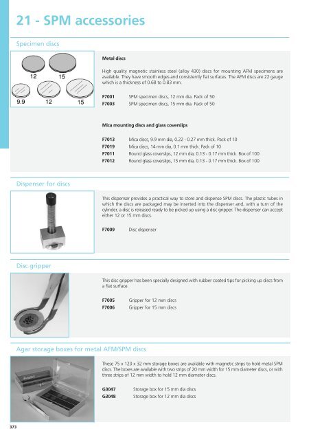
Specimen discs<br />
Metal discs<br />
High quality magnetic stainless steel (alloy 430) discs for mounting AFM specimens are<br />
available. They have smooth edges and consistently flat surfaces. The AFM discs are 22 gauge<br />
which is a thickness of 0.68 to 0.83 mm.<br />
F7001 <strong>SPM</strong> specimen discs, 12 mm dia. Pack of 50<br />
F7003 <strong>SPM</strong> specimen discs, 15 mm dia. Pack of 50<br />
Mica mounting discs and glass coverslips<br />
F7013 Mica discs, 9.9 mm dia, 0.22 - 0.27 mm thick. Pack of 10<br />
F7019 Mica discs, 14 mm dia, 0.1 mm thick. Pack of 10<br />
F7011 Round glass coverslips, 12 mm dia, 0.13 - 0.17 mm thick. Box of 100<br />
F7012 Round glass coverslips, 15 mm dia, 0.13 - 0.17 mm thick. Box of 100<br />
Dispenser for discs<br />
This dispenser provides a practical way to store and dispense <strong>SPM</strong> discs. The plastic tubes in<br />
which the discs are packaged may be inserted into the dispenser and, with a turn of the<br />
cylinder, a disc is released ready to be picked up using a disc gripper. The dispenser can accept<br />
either 12 or 15 mm discs.<br />
F7009<br />
Disc dispenser<br />
Disc gripper<br />
This disc gripper has been specially designed with rubber coated tips for picking up discs from<br />
a flat surface.<br />
F7005<br />
F7006<br />
Gripper for 12 mm discs<br />
Gripper for 15 mm discs<br />
<strong>Agar</strong> storage boxes for metal AFM/<strong>SPM</strong> discs<br />
These 75 x 120 x 32 mm storage boxes are available with magnetic strips to hold metal <strong>SPM</strong><br />
discs. The boxes are available with two strips of 20 mm width for 15 mm diameter discs, or with<br />
three strips of 12 mm width to hold 12 mm diameter discs.<br />
G3047<br />
G3048<br />
Storage box for 15 mm dia discs<br />
Storage box for 12 mm dia discs<br />
373
<strong>SPM</strong> <strong>accessories</strong><br />
Disc carrier and pick-up tool<br />
These disc carriers provide practical dust-free storage for 12 and 15 mm <strong>SPM</strong> discs. Discs are<br />
placed face down into a stepped cavity, which prevents damage to the specimen. The sliding<br />
cover secures the disc in position.<br />
F7007<br />
F7008<br />
Disc carrier for ten 12 mm discs<br />
Disc carrier for eight 15 mm discs<br />
Magnetic pick-up tool<br />
This convenient magnetic tool is useful for picking up and manoeuvring <strong>SPM</strong> discs without damage<br />
to mounted specimens.<br />
F7010<br />
Magnetic pick-up tool<br />
Highly ordered pyrolytic graphite (HOPG)<br />
HOPG is widely used as a substrate for specimens to be examined in scanning probe microscopy.<br />
It is also used as a calibration specimen and cleaves almost like mica because of its layered<br />
structure. Unlike mica, HOPG is non-polar and, for samples where elemental analysis is required,<br />
it provides a carbon-only background. It consists of highly ordered planes of carbon atoms in<br />
(002) orientation and the quality of these parallel planes is defined by the mosaic spread angle.<br />
The standard grade of HOPG has a mosaic angle of 3.5° ± 1.5°, while substrates with more<br />
highly ordered planes, with mosaic angles of 0.8° ± 0.2° and 0.4° ± 0.1°, are also available.<br />
G3389 HOPG mosaic spread 3.5° ± 1.5°, 10 x 10 x 2 mm<br />
G3389-1<strong>21</strong>2 HOPG mosaic spread 3.5° ± 1.5°, 12 x 12 x 2 mm<br />
G3389-1717 HOPG mosaic spread 3.5° ± 1.5°, 17 x 17 x 2 mm<br />
G3046-55 HOPG mosaic spread 0.8° ± 0.2°, 5 x 5 x 1 mm<br />
G3046-1010 HOPG mosaic spread 0.8° ± 0.2°, 10 x 10 x 1 mm<br />
G3045-55 HOPG mosaic spread 0.4° ± 0.1°, 5 x 5 x 1 mm<br />
G3045-1010 HOPG mosaic spread 0.4° ± 0.1°, 10 x 10 x 1 mm<br />
Other sizes are available on request.<br />
Diamond knives for AFM<br />
High quality diamond knives are useful for surface sections of all kinds of biological and industrial<br />
specimens for AFM investigation.<br />
For further details of diamond knives, please refer to section 14.<br />
Tel: +44 (0)1279 813519 Fax: +44 (0)1279 815106 Email: sales@agarscientific.com www.agarscientific.com 374
<strong>SPM</strong> <strong>accessories</strong><br />
Mica<br />
Freshly cleaved ruby muscovite mica surfaces are extremely even and flat. They are also quite<br />
transparent and free from scratches and contamination. Cleaved mica is traditionally used in<br />
electron microscopy for the production of carbon support films, cell growing and thin film<br />
coating research. Ruby muscovite mica surfaces are also suitable as substrates for high<br />
resolution atomic force microscopy studies of DNA and DNA-protein complexes.<br />
The mica cleaving process involves insertion of a sharp edge or point into an edge or corner<br />
of the mica sheet and gently separating the natural layers of the mica. A thin double edged<br />
razor blade is extremely good for this purpose.<br />
The freshly exposed cleaved surface should be used immediately to utilise the clean and even<br />
surface. The starting thickness of the mica sheets varies between 0.10 and 0.25 mm. The<br />
minimum thickness is dependant on the skill of the person doing the cleaving.<br />
Ruby muscovite is a hard material with excellent cleaving properties. It has a minimal tendency<br />
to cracking and splits more easily into thin films along natural cleavage planes.<br />
G250-3 Mica 11 x 11 mm, 0.15 mm thick. Pack of 20<br />
G250-2 Mica 25 x 25 mm, 0.15 mm thick. Pack of 20<br />
G250-1 Mica 75 x 25 mm, 0.15 mm thick. Pack of 20<br />
G250-4 Mica 100 x 20 mm, 0.15 mm thick. Pack of 20<br />
G250-5 Mica 150 x 150 mm, 0.15 mm thick. Pack of 3<br />
G250-6 Mica 9.9 mm dia, 0.1 mm thick, ultra-clean. Pack of 10<br />
G250-7 Mica 20 x 20 mm, 0.25 mm thick, ultra-clean. Pack of 10<br />
Other sizes are available on request.<br />
Crossed grating replica<br />
This crossed-line grating replica has <strong>21</strong>60 lines/mm, and can be used for X, Y axis calibration.<br />
F7016<br />
F7017<br />
Crossed grating replica on 12 mm disc<br />
Crossed grating replica, unmounted<br />
Gold calibration kit<br />
Gold colloids of known size provide a reliable means of characterising tip geometry and calibrating the<br />
Z-axis to piezoelectric response. The incompressible, monodispersive and spherical nature of the colloids<br />
can also be used to characterise the vertical dimension of co -adsorbed biomolecules. The standard kit<br />
has colloids of 5, 15 and 30 nm diameter, eight numbered mica-coated 15 mm discs, a disc carrier and<br />
a magnetic pick-up tool. The extended kit contains additional colloids of 10 and 20 nm diameter.<br />
F7020<br />
F7018<br />
Standard gold calibration kit<br />
Extended gold calibration kit<br />
375
<strong>SPM</strong> <strong>accessories</strong><br />
Silicon calibration gratings<br />
A range of ultra-sharp silicon gratings for calibration and distortion checking of scanning probe microscopes is available. Gratings with<br />
different profiles have been manufactured using microfabrication techniques.<br />
Individual gratings can also be supplied as sets; see page 378.<br />
Porous aluminium tip characterisation structure<br />
This thin film porous aluminium test structure consists of hexagonal hollow cells. The film is 500 µm thick<br />
with 40 nm pore depth, and has an active area of 3 x 3 mm. The thickness of the partitions between<br />
the pores is about 5 nm. The radius of the spikes formed at the intersections of the partitions is<br />
approximately 2 nm, which is extremely useful for characterisation of AFM tip shape. In order not to<br />
damage the spikes of the grating, scanning should be performed in tapping mode because hard<br />
cantilevers in contact mode may break off the spikes.<br />
Cat. no. Grating type Pore depth, nm Pitch*, nm Accuracy, nm<br />
F7030 PA01 40 100 ± 10<br />
* Value for information only, not for vertical calibration purposes<br />
Grating type TGZ<br />
The calibration gratings from the TGZ series are 1-D arrays of rectangular SiO2 steps on a silicon wafer.<br />
The structure is coated with Si3N4 to protect the silicon from oxidation. The step height value is calibrated<br />
over the whole active area.<br />
Gratings are available with nominal heights ranging between 20 nm and 1.5 µm, with an active area of<br />
3 x 3 mm on chips of 5 x 5 x 0.45 mm. The 1.5 µm grating has a pitch of 10 µm, while the others have<br />
a pitch of 3.0 µm.<br />
10 µm<br />
Cat. no. Grating type Step height Range, nm Accuracy<br />
F70<strong>21</strong> TGZ01 20 nm 18 - 26 ± 1 nm<br />
F7022 TGZ02 100 nm 94 - 106 ± 1.5 nm<br />
F7023 TGZ03 500 nm 490 - 520 ± 1 %<br />
F7031 TGZ04 1 µm 900 - 1100 ± 1 %<br />
F7032 TGZ11 1.5 µm 1350 - 1650 ± 1 %<br />
NIST traceable gratings of types TGZ01, TGZ02 and TGZ03, which have been individually controlled and certified with an AFM<br />
calibrated using NIST certified reference standards, are also available.<br />
F70<strong>21</strong>C<br />
F7022C<br />
F7023C<br />
NIST traceable grating TGZ01<br />
NIST traceable grating TGZ02<br />
NIST traceable grating TGZ03<br />
Tel: +44 (0)1279 813519 Fax: +44 (0)1279 815106 Email: sales@agarscientific.com www.agarscientific.com 376
<strong>SPM</strong> <strong>accessories</strong><br />
Grating type TGG<br />
The TGG01 silicon calibration grating is a 1-D array of triangular steps having precise linear and angular<br />
dimensions defined by the crystallography of silicon ((111) plane) and maintained with high accuracy.<br />
The edges of the triangular steps have curvature radii less than 10 nm. This type of calibration grating<br />
can be used for lateral calibration, non-linearity detection, assessment of angular distortion and<br />
determining the radius of curvature of cantilever tips. The silicon grating has an active area of<br />
3 x 3 mm on chips of 5 x 5 x 0.45 mm.<br />
1.0 µm<br />
Cat. no. Grating type Step height*, µm Pitch, µm Accuracy, nm<br />
F7024 TGG01 1.8 3.0 ± 5<br />
* Step height for information only, not for vertical calibration purposes<br />
Grating type TGX<br />
The TGX series silicon calibration grating is a chequerboard-like array of square pillars with sharp<br />
undercut edges formed by the (110) crystallographic planes of silicon. The typical radius of the<br />
edges is less than 5 nm. TGX calibration gratings are intended for lateral calibration of <strong>SPM</strong> scanners,<br />
and can be used as test structures for the detection and correction of lateral non- linearity, hysteresis,<br />
and creep and cross-coupling effects. It can also be used for the determination of the tip aspect ratio.<br />
The grating has an active area of 2 x 2 mm on chips of 5 x 5 x 0.45 mm.<br />
1.0 µm<br />
Cat. no. Grating type Step height*, µm Pitch, µm Accuracy<br />
F7026 TGX01 1.8 3.0 ± 8 nm<br />
F7033 TGX11 1.8 10.0 ± 0.25 %<br />
* Step height for information only, not for vertical calibration purposes<br />
Grating type TGF<br />
The TGF11 silicon calibration grating is a 1-D array of trapezoidal steps with a 10 µm pitch and<br />
height of approximately 1.75 µm. The lateral faces of the steps have an inclination angle with respect<br />
to the horizontal plane of precisely arctan √2 (54° 74'). This angle is defined by the crystallography<br />
of silicon and is maintained with high accuracy. The grating has an active area of 3 x 3 mm on chips<br />
of 5 x 5 x 0.45 mm.<br />
10 µm<br />
This grating can be used for the assessment of scanner non-linearity in the vertical direction.<br />
Direct calibration of the lateral force can be obtained by analysing the contact response measured<br />
on the flat and sloped facet. This can be done for the calibration of conventional Si probes or<br />
cantilevers with an attached colloidal particle with any radius of curvature up to 2 µm.<br />
Cat. no. Grating type Step height, µm* Pitch, µm Accuracy Edge angle<br />
F7027 TGF11 1.75 10.0 ± 0.25 % 54° 74’<br />
* Step height for information only, not for vertical calibration purposes<br />
377
<strong>SPM</strong> <strong>accessories</strong><br />
Calibration grating sets TGS<br />
Sets of calibration gratings and test structures are available to suit different requirements.<br />
Set F7034 is for vertical calibration only, and the F7034C calibrated set is traceable to NIST.<br />
Set F7036 is for tip characterisation and lateral calibration only.<br />
Set F7035 is the most comprehensive set of gratings and test structures, combining F7034 and F7036 to allow lateral calibration, vertical<br />
calibration and tip characterisation.<br />
Set F7035C makes the vertical calibration traceable to NIST.<br />
PA01, F7030<br />
TGX, F7026<br />
TGG, F7024<br />
TGZ, F70<strong>21</strong>/2/3<br />
Cat. no.<br />
Grating type<br />
PA01 TGX01 TGG01 TGZ01 TGZ02 TGZ03<br />
F7034 F70<strong>21</strong> F7022 F7023<br />
F7035 F7030 F7026 F7024 F70<strong>21</strong> F7022 F7023<br />
F7036 F7030 F7026 F7024<br />
F7034C* F70<strong>21</strong> F7022 F7023<br />
F7035C* F7030 F7026 F7024 F70<strong>21</strong> F7022 F7023<br />
* Calibration traceable to NIST<br />
Gold-coated substrates<br />
PLATYPUS gold-coated substrates are prepared in an electron beam evaporator in a dedicated<br />
clean environment, to prevent contamination of the gold film, and using a titanium adhesion<br />
layer on plasma-cleaned surfaces. Substrates of mica, silicon, aluminosilicate glass slides and<br />
coverslips are available, with a range of thicknesses of gold film.<br />
The gold-coated mica and aluminosilicate glass slides can be flame-annealed for atomically flat<br />
terraces and enhanced (111) orientation, that can be used in many surface science fields,<br />
including electrochemistry, biosensors and nanowetting.<br />
F7040<br />
F7041<br />
Mica 1 x 1.5″, with 200 nm gold<br />
Mica 1 x 3″, with 200 nm gold<br />
F7042 Silicon wafers 4″ dia, with 100 nm gold. Pack of 3<br />
F7043 Silicon wafers 4″ dia, with 100 nm gold. Pack of 12<br />
F7044 Aluminosilicate glass slides 1 x 3″, 0.7 mm thick, with 10 nm gold. Pack of 5<br />
F7045 Aluminosilicate glass slides 1 x 3″, 0.7 mm thick, with 50 nm gold. Pack of 5<br />
F7046 Aluminosilicate glass slides 1 x 3″, 0.7 mm thick, with 100 nm gold. Pack of 5<br />
F7047 Coverslips 22 mm square, 0.13 - 0.16 mm thick, with 10 nm gold. Pack of 12<br />
F7048 Coverslips 22 mm square, 0.13 - 0.16 mm thick, with 50 nm gold. Pack of 12<br />
F7049 Coverslips 15 mm dia circular, 0.13 - 0.16 mm thick, with 10 nm gold. Pack of 24<br />
Tel: +44 (0)1279 813519 Fax: +44 (0)1279 815106 Email: sales@agarscientific.com www.agarscientific.com 378
<strong>SPM</strong> <strong>accessories</strong><br />
Arrandee gold-coated substrates<br />
Arrandee gold-coated substrates use a borosilicate glass base of 0.7 mm thickness. They are<br />
suitable for easy preparation of gold terraces and by simple flame annealing 100 x 100 nm<br />
Au (111) terraces can easily be obtained.<br />
A thin layer of chromium, 1 to 4 nm, is applied to the glass surface. This layer guarantees<br />
optimum adhesion to the glass as well as to the subsequently deposited gold layer<br />
(250 nm ± 50 nm). Arrandee substrates are very useful for <strong>SPM</strong> investigations.<br />
F7037-25 Gold coated substrates, 11 x 11 mm. Pack of 25<br />
F7037 Gold coated substrates, 11 x 11 mm. Pack of 50<br />
F7038 Gold coated substrates, 12 x 12 mm. Pack of 50<br />
Silicon nitride coated discs (blanks)<br />
These 200 µm thick 3 mm silicon support discs have a low stress, ultra-flat 50 nm layer of<br />
silicon nitride on both sides. The film is non-stoichiometric and is closer to SiN than Si3N4. The<br />
discs are perfectly round and free of debris, with a specially designed edge for ease of handling.<br />
The discs have a mean surface roughness of 0.45 nm ± 0.2 nm. They can be used for a number<br />
of applications, including as specimen discs for AFM and also as specimen mounts for SEM and<br />
FESEM. Silicon nitride coated discs are also available with a hydrophilic surface coating which<br />
consists of a 5 nm atomic layer of hydroxylated aluminium deposited onto the membrane<br />
surface.<br />
Supplied in packs of 10.<br />
G3343 Silicon nitride discs, 3 mm dia. Pack of 10<br />
G3343H Silicon nitride discs with hydrophilic coating, 3 mm dia. Pack of 10<br />
MetroChip calibration standard<br />
The MetroChip microscope calibration standard provides an extensive range of features for SEM,<br />
FIB, AFM, light microscopy and metrology systems calibration. It is supplied on a 20 x 20 mm chip<br />
with a thickness of 750 µm, with periodic features for enhanced calibration in the range 4 mm<br />
down to 100 nm.<br />
The MetroChip can also be used for AFM and light microscopy and includes a number of features<br />
to check linearity, distortion and scan length.<br />
The SEM calibration feature includes alignment marks, linear microscale, distortion<br />
measurements, paraxial calibration (image shift), resolution measurements, focus star, stigmator<br />
calibration, gratings, and concentric circles and squares. The combination of these features on<br />
one standard makes the MetroChip ideal as an all-in-one standard both for initial set up and<br />
regular calibration checks. Due to its composition, the chip exhibits minimal charging and, if<br />
cared for properly, a long sample life.<br />
The MetroChip standard is easy to navigate and comes with dimension labels on most features.<br />
It is fully traceable to NIST certification.<br />
S1949<br />
MetroChip calibration standard, certified<br />
379
<strong>SPM</strong> <strong>accessories</strong><br />
Critical dimension (CD) calibration test specimens<br />
A CD calibration test specimen is of particular interest to microscopists and test engineers using high performance SEMs for critical<br />
measurement of semiconductor line width dimensions.<br />
The 4.8 x 4.8 mm silicon standard has a series of chequerboard patterns around its edges with a side length of 480 µm. These can be<br />
used for optimising imaging parameters and checking distortion.<br />
The central region of the standard contains a series of five line patterns, each one clearly identified with its pitch size. Each pattern is<br />
made up of five bars and spaces of equal width. Bar pitch for the individual patterns range in size from 0.5 to 10 µm for calibrating<br />
intermediate size structures and 100 to 500 nm for smaller structures. Each standard is identified by a unique serial number.<br />
The test specimen is available as non-certified, or certified by the German Physikalisch -Technische Bundesanstalt. For certified standards,<br />
each pitch is measured and a mean value calculated from a series of five measurements. Measurements were made on a dedicated CD<br />
measuring system fitted to a FEG SEM at an accelerating voltage of 700 eV.<br />
10-5-2-1-0.5 µm structure<br />
This CD calibration test specimen comprises five line patterns, each one clearly identified by its pitch.<br />
Each pattern has five bars and spaces of equal pitch: 10, 5, 2, 1 and 0.5 µm. The central line area<br />
can be used for AFM measurements. The patterns are etched into silicon with a depth of<br />
approximately 200 µm. There is no coating on the silicon surface.<br />
S1995A<br />
S1997A<br />
CD calibration specimen, 10-5-2-1-0.5 µm, non-certified<br />
CD calibration specimen, 10-5-2-1-0.5 µm, certified<br />
Each standard is identified by a unique serial number.<br />
The specimen can be supplied unmounted or mounted on any of the standard range of SEM stubs. Please specify.<br />
500-200-100 nm structure<br />
This advanced CD calibration test specimen is suitable for calibrating smaller structures. It comprises<br />
three line patterns, each identified by its pitch. Each pattern has five bars and spaces of equal pitch:<br />
500, 200 and 100 nm. The central line area can be used for AFM measurements. The patterns are<br />
etched into silicon with a depth of approximately 45 to 50 nm. There is no coating on the silicon<br />
surface.<br />
S1998<br />
S1998A<br />
CD calibration specimen, 500-200-100 nm, non-certified<br />
CD calibration specimen, 500-200-100 nm, certified<br />
Each standard is identified by a unique serial number.<br />
The specimen can be supplied unmounted or mounted on any of the standard range of SEM stubs. Please specify.<br />
Tel: +44 (0)1279 813519 Fax: +44 (0)1279 815106 Email: sales@agarscientific.com www.agarscientific.com 380
<strong>SPM</strong> <strong>accessories</strong><br />
High magnification, high resolution calibration reference<br />
and traceable standard for SEM, AFM, Auger and FIB<br />
This precision, holographic pattern is highly accurate and stable, with moderate ridge heights that are convenient for AFM. This specimen<br />
provides excellent contrast for secondary and back scatter imaging with SEM. It provides accurate calibration for high resolution,<br />
nanometer-scale measurements. These are available with 70, 145 and 292 nm pitch.<br />
Reference standards for AFM calibration are mounted on a 12 mm steel AFM disc, and can be used in contact, tapping and other<br />
modes with image sizes from 100 nm to 3 µm. Standards for SEM can be supplied unmounted or mounted on an SEM stub of choice,<br />
and can be used for a wide range of accelerating voltages (1 - 20 kV) calibrating images from x25,000 to x1,000,000. The traceable,<br />
certified standards conform to the German Physikalisch -Technische Bundesanstalt, and subsequently NIST.<br />
High resolution AFM reference standards, certified<br />
F7053<br />
F7053T<br />
F7054<br />
F7054U<br />
F7055<br />
F7055T<br />
70 nm AFM reference standard, non-traceable, on 12 mm steel disc<br />
70 nm AFM reference standard, traceable, on 12 mm steel disc<br />
145 nm AFM reference standard, non-traceable, on 12 mm steel disc<br />
145 nm AFM reference standard, non-traceable, unmounted<br />
292 nm AFM reference standard, non-traceable, on 12 mm steel disc<br />
292 nm AFM reference standard, traceable, on 12 mm steel disc<br />
1 µm AFM scan<br />
For details of these products, please refer to section 3, pages 63 - 65.<br />
2-D holographic array standards<br />
These 2-D holographic array standards for simultaneous calibration of X and Y axes have unique<br />
characteristics that make them especially easy to use. The pitch is less than 500 nm and the pattern covers<br />
the entire die so there is no need to hunt for the scan area. The array of bumps means that the image<br />
contrast is high even when the probe tip is slightly dull. The patterns are durable and allow for high contrast<br />
scanning in contact mode so that calibration and measurements are faster. They can be used in contact,<br />
intermittent contact (TappingMode) and other modes with image sizes from 250 nm to 10 mm.<br />
AFM 144 nm reference standards, certified, non-traceable, mounted on disc<br />
F7050<br />
144 nm 2-D pattern calibration standard on 12 mm steel disc<br />
AFM 144 nm reference standards, certified (certificate provided), traceable, mounted on disc<br />
F7051<br />
144 nm 2-D UTC pattern calibration standard on 12 mm steel disc<br />
AFM 300 nm reference standards, certified, non-traceable, mounted on disc<br />
F7052<br />
300 nm 2-D resolution AFM reference standard on 12 mm steel disc<br />
For more details, please refer to section 3, pages 61 - 62.<br />
381
<strong>SPM</strong> <strong>accessories</strong><br />
Geller reference standards MRS-3, MRS-4 and MRS-5<br />
MRS-3, MRS-4 and MRS-5 are a series of standards that are available for use with all scanning probe<br />
microscopies. These standards have fine dimensional pitch patterns. The 80 nm pitch has a nominal<br />
space width of 40 nm and a pattern height of 0.1 µm and therefore the cantilever tip must be smaller<br />
to define the pattern.<br />
S1990<br />
S1991<br />
S1992<br />
S1993<br />
MRS-3 reference standard, non-certified<br />
MRS-3XY certified standard, NPL and NIST traceable<br />
MRS-3XYZ certified standard, NPL and NIST traceable in X, Y<br />
with Z calibration NIST traceable<br />
MRS-3 reference standard, non-certified 3 mm dia<br />
Please add suffix S for universal holder and O for optical holder for mounted specimens.<br />
S1810<br />
S1811<br />
S1812<br />
S1813<br />
MRS-4 reference standard, non-certified<br />
MRS-4XY certified standard, NPL and NIST traceable<br />
MRS-4XYZ certified standard, NPL and NIST traceable in X, Y<br />
with Z calibration NIST traceable<br />
MRS-4 reference standard, non-certified 3 mm dia<br />
Please add suffix S for universal holder and O for optical holder for mounted specimens.<br />
S1814 MRS-5 reference standard, non-certified<br />
S1815 MRS-5XY certified standard, NPL and NIST traceable<br />
Please add suffix -S for universal holder and -O for optical holder for mounted specimens.<br />
For more details, please refer to section 3, pages 59 - 60.<br />
Kleindiek SuperFlat Atomic Force Microscope<br />
The SuperFlat Atomic Force Microscope (SF-AFM) is an addition to the range of load-lockable<br />
tools which offers a high resolution AFM solution for work inside an SEM. Based on the<br />
Shuttle platform used by the Prober Shuttle, the SF-AFM consists of a next generation<br />
nanomanipulator in combination with a super flat piezo scanner. The manipulator is used for<br />
coarse positioning of the cantilever tip. Once the area of interest has been located with the<br />
help of the SEM, and the cantilever has been brought into position, scanning is performed<br />
using the piezo scanner to which the sample is mounted. By using a compact and flexible<br />
AFM inside the SEM, information on lateral dimensions from SEM inspection can be<br />
complemented by precise topographical and force information.<br />
For further details, please refer to section 20.<br />
Tel: +44 (0)1279 813519 Fax: +44 (0)1279 815106 Email: sales@agarscientific.com www.agarscientific.com 382