Create successful ePaper yourself
Turn your PDF publications into a flip-book with our unique Google optimized e-Paper software.
<strong>nRF24LU1</strong> <strong>Development</strong> <strong>Kit</strong> <strong>User</strong> <strong>Guide</strong><br />
The Radio Modules for the <strong>nRF24LU1</strong> Embedded 2.4GHz Transceiver with USB has been developed<br />
to enable customers to test functionality, run communication and verify the performance parameters<br />
of the device. The <strong>nRF24LU1</strong> Radio Modules comes with the <strong>nRF24LU1</strong> DEVKIT .The modules come<br />
in two versions; one with a SMA connector and one with a quarter wave PCB antenna. The module<br />
with SMA connector is developed to make it easy to do conducted measurements to test the<br />
performance of the radio. Except for the antenna, the modules have the same layout and same Bill of<br />
Material.<br />
The <strong>nRF24LU1</strong> Radio Modules are intended for evaluation and development purposes only.<br />
11.5 <strong>nRF24LU1</strong> Radio Module hardware description<br />
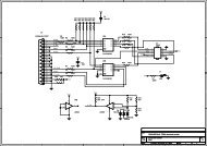
Figure 22 to Figure 25 shows the <strong>nRF24LU1</strong> Radio Modules circuit diagrams and PCB layouts. The<br />
BOM is given in Table 8.<br />
The module has the <strong>nRF24LU1</strong> and all necessary circuit to start using the <strong>nRF24LU1</strong>. It plugs into the<br />
40 pin DIL connector of the Basic Feature Board (BFB). All I/Os are then available on the Basic<br />
Feature Board.<br />
11.5.1 Debugger interface<br />
To use the built in debugger of the <strong>nRF24LU1</strong>, a JTAG/FS2 interface, J2, is available on the module.<br />
J2 pin<br />
1 TCK<br />
2 GND<br />
3 TDO<br />
4 VDD<br />
5 TMS<br />
6 VDD<br />
7 Trig out / P0.4<br />
8 RESET<br />
9 TDI<br />
10 Not used<br />
Table 6 - FS2 Debug Interface<br />
JTAG/FS4 name<br />
11.5.2 Led drivers<br />
LED 1-3 on the BFB is driven with LED drivers on the Radio Module<br />
11.5.3 Power Supply Switch<br />
The switch S1 can be used to switch the power supply between the battery pack on the BFB for stand<br />
alone use, or to VBUS from the USB connector.<br />
11.5.4 Flash programming<br />
The FLASH in the <strong>nRF24LU1</strong> can be programmed from the “ISP Interface” connector on the BFB by<br />
using the ISP Dongle<br />
Note: The JTAG connector on the Radio Modules is not pin compatible with the ISP Dongle from<br />
Nordic Semiconductor and can not be used to program the flash.<br />
11.5.5 Antenna<br />
For connection of a single ended antenna or to any 50Ω test equipment, the <strong>nRF24LU1</strong> Radio Module<br />
with the SMA connector can be used.<br />
Revision 1.0 Page 32 of 36


