Create successful ePaper yourself
Turn your PDF publications into a flip-book with our unique Google optimized e-Paper software.
<strong>nRF24LU1</strong> <strong>Development</strong> <strong>Kit</strong> <strong>User</strong> <strong>Guide</strong><br />
11.2.3 Buttons<br />
There are three buttons on the <strong>nRF24LU1</strong> <strong>Development</strong> <strong>Kit</strong> BFB that are connected to the<br />
<strong>nRF24LU1</strong>. These are used to give input to the MCU during tests. The function of these buttons<br />
depends on the firmware on the <strong>nRF24LU1</strong><br />
11.2.4 Rotary Switch<br />
The rotary switch is not used when the BFB is used with the <strong>nRF24LU1</strong> Radio Module.<br />
11.2.5 SPI Interface<br />
This connector is used to program the FLASH on the <strong>nRF24LU1</strong>. The ISP dongle is then connected<br />
here. The pin out of this connector is shown in Table 1.<br />
Pin Number Signal name Description<br />
1 RF_VDD Supply voltage<br />
2 Not used<br />
3 RESET Reset signal to <strong>nRF24LU1</strong><br />
4 CSN SPI CSN<br />
5 MISO SPI MISO<br />
6 PROG PROG signal from <strong>nRF24LU1</strong><br />
7 MOSI SPI MOSI<br />
8 SCK SPI SCK<br />
9 Not used<br />
10 GND Common ground<br />
Table 1 - Pinout of the SPI Interface connector<br />
11.2.6 Module connector<br />
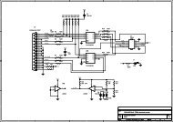
A 40 pin dual in line socket, J1, is used to connect the <strong>nRF24LU1</strong> Radio Module to the BFB. The pin<br />
out for this connector is given in Table 2.<br />
Pin Number Signal name Description Connected to<br />
1 GND Common ground<br />
2 LED1 Led driver on Radio Module, LED 1<br />
P0.0<br />
3 LED2 Led driver on Radio Module, LED 2<br />
P0.1<br />
4 LED3 Led driver on Radio Module, LED 3<br />
P0.2<br />
5 Not used LED 4<br />
6 Not used<br />
7 Not used<br />
8 Not used<br />
9 Not used<br />
10 GND Common ground<br />
11 Not used<br />
12 P0.5 GPIO P0.5 Button B1<br />
13 P0.4 GPIO P0.4 Button B2<br />
14 P0.3/CSN GPIO P0.3 or SPI CSN Button B3<br />
15 Not used<br />
16 Not used<br />
17 Not used<br />
Revision 1.0 Page 26 of 36


