LM5020 100V Current Mode PWM Controller
LM5020 100V Current Mode PWM Controller
LM5020 100V Current Mode PWM Controller

You also want an ePaper? Increase the reach of your titles
YUMPU automatically turns print PDFs into web optimized ePapers that Google loves.
<strong>LM5020</strong><br />
<strong>100V</strong> <strong>Current</strong> <strong>Mode</strong> <strong>PWM</strong> <strong>Controller</strong><br />
General Description<br />
The <strong>LM5020</strong> high voltage pulse-width-modulation (<strong>PWM</strong>)<br />
controller contains all of the features needed to implement<br />
single ended primary power converter topologies. Output<br />
voltage regulation is based on current-mode control, which<br />
eases the design of loop compensation while providing inherent<br />
line feed-forward. The <strong>LM5020</strong> includes a highvoltage<br />
start-up regulator that operates over a wide input<br />
range up to <strong>100V</strong>. The <strong>PWM</strong> controller is designed for high<br />
speed capability including an oscillator frequency range to<br />
1MHz and total propagation delays less than 100ns. Additional<br />
features include an error amplifier, precision reference,<br />
line under-voltage lockout, cycle-by-cycle current limit, slope<br />
compensation, softstart, oscillator synchronization capability<br />
and thermal shutdown. The controller is available in both<br />
MSOP-10 and LLP-10 packages.<br />
Features<br />
n Internal Start-up Bias Regulator<br />
n Error Amplifier<br />
n Precision Voltage Reference<br />
n Programmable Softstart<br />
n 1A Peak Gate Driver<br />
n Maximum Duty Cycle Limiting (80% for <strong>LM5020</strong>-1 or<br />
50% for <strong>LM5020</strong>-2)<br />
n Programmable Line Under Voltage Lockout (UVLO) with<br />
Adjustable Hysteresis<br />
n Cycle-by-Cycle Over-<strong>Current</strong> Protection<br />
n Slope Compensation (<strong>LM5020</strong>-1)<br />
n Programmable Oscillator Frequency with<br />
Synchronization Capability<br />
n <strong>Current</strong> Sense Leading Edge Blanking<br />
n Thermal Shutdown Protection<br />
Packages<br />
n MSOP-10<br />
n LLP-10 (4 mm x4mm)<br />
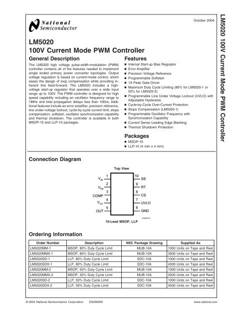
October 2004<br />
<strong>LM5020</strong> <strong>100V</strong> <strong>Current</strong> <strong>Mode</strong> <strong>PWM</strong> <strong>Controller</strong><br />
Connection Diagram<br />
Top View<br />
10-Lead MSOP, LLP<br />
20095001<br />
Ordering Information<br />
Order Number Description NSC Package Drawing Supplied As<br />
<strong>LM5020</strong>MM-1 MSOP, 80% Duty Cycle Limit MUB-10A 1000 Units on Tape and Reel<br />
<strong>LM5020</strong>MMX-1 MSOP, 80% Duty Cycle Limit MUB-10A 3500 Units on Tape and Reel<br />
<strong>LM5020</strong>SD-1 LLP, 80% Duty Cycle Limit SDC-10A 1000 Units on Tape and Reel<br />
<strong>LM5020</strong>SDX-1 LLP, 80% Duty Cycle Limit SDC-10A 4500 Units on Tape and Reel<br />
<strong>LM5020</strong>MM-2 MSOP, 50% Duty Cycle Limit MUB-10A 1000 Units on Tape and Reel<br />
<strong>LM5020</strong>MMX-2 MSOP, 50% Duty Cycle Limit MUB-10A 3500 Units on Tape and Reel<br />
<strong>LM5020</strong>SD-2 LLP, 50% Duty Cycle Limit SDC-10A 1000 Units on Tape and Reel<br />
<strong>LM5020</strong>SDX-2 LLP, 50% Duty Cycle Limit SDC-10A 4500 Units on Tape and Reel<br />
© 2004 National Semiconductor Corporation DS200950 www.national.com
<strong>LM5020</strong><br />
Block Diagram<br />
20095002<br />
FIGURE 1.<br />
www.national.com 2
Pin Description<br />
PIN NAME DESCRIPTION APPLICATION INFORMATION<br />
1 Vin Source Input Voltage Input to start-up regulator. Input range<br />
13V to <strong>100V</strong>.<br />
2 FB Feedback Signal Inverting input of the internal error<br />
amplifier. The non-inverting input is<br />
internally connected to a 1.25V<br />
reference.<br />
3 COMP The output of the error<br />
amplifier and input to the<br />
Pulse Width Modulator<br />
4 V CC Output of the internal high<br />
voltage series pass regulator.<br />
Regulated output voltage 7.7V<br />
COMP pull-up is provided by an<br />
internal 5K resistor which may be<br />
used to bias an opto-coupler<br />
transistor.<br />
If an auxiliary winding raises the<br />
voltage on this pin above the<br />
regulation set point, the internal series<br />
pass regulator will shutdown, reducing<br />
the controller power dissipation.<br />
5 OUT Output of the <strong>PWM</strong> controller Gate driver output with a 1A peak<br />
current capability<br />
6 GND Ground return<br />
7 UVLO Line Under-Voltage Shutdown An external resistor divider from the<br />
power converter source sets the<br />
shutdown levels. The threshold of<br />
operation equals 1.25V. Hysteresis is<br />
set by a switched internal 20µA<br />
current source.<br />
8 CS <strong>Current</strong> Sense input <strong>Current</strong> sense input for current mode<br />
control and over-current protection.<br />
<strong>Current</strong> limiting is accomplished using<br />
a dedicated current sense comparator.<br />
If the CS comparator input exceeds<br />
0.5V the OUT pin switches low for<br />
cycle-by-cycle current limiting. CS is<br />
held low for 50ns after OUT switches<br />
high to blank leading edge current<br />
spikes.<br />
9 RT / SYNC Oscillator timing resistor pin<br />
and synchronization input<br />
An external resistor connected from<br />
RT to GND sets the oscillator<br />
frequency. This pin will also accept<br />
synchronization pulses from an<br />
external clock.<br />
10 SS Softstart Input An external capacitor and an internal<br />
10µA current source set the soft-start<br />
ramp rate.<br />
<strong>LM5020</strong><br />
3<br />
www.national.com
<strong>LM5020</strong><br />
Absolute Maximum Ratings (Note 1)<br />
If Military/Aerospace specified devices are required,<br />
please contact the National Semiconductor Sales Office/<br />
Distributors for availability and specifications.<br />
V IN to GND<br />
-0.3V to <strong>100V</strong><br />
V CC to GND<br />
-0.3V to 16V<br />
RT to GND -0.3V to 5.5V<br />
All other pins to GND<br />
-0.3V to 7V<br />
Storage Temperature<br />
Junction Temperature<br />
Operating Ratings<br />
V IN Voltage<br />
External Voltage applied to V CC<br />
Operating Junction Temperature<br />
-55˚C to +150˚C<br />
150˚C<br />
13V to 90V<br />
8V to 15V<br />
-40˚C to +125˚C<br />
Power Dissipation<br />
Internally Limited<br />
ESD Rating (Note 2)<br />
Human Body <strong>Mode</strong>l<br />
2kV<br />
Electrical Characteristics<br />
Specifications in standard type face are for T J = +25˚C and those in boldface type apply over the full operating junction temperature<br />
range. Unless otherwise specified: V IN = 48V, V CC = 10V, and RT = 31.6KΩ<br />
Symbol Parameter Conditions Min Typ Max Units<br />
Startup Regulator<br />
V CC Reg V CC Regulation Open ckt 7.4 7.7 8.0 V<br />
V CC <strong>Current</strong> Limit (Note 4) 15 22 mA<br />
I-V IN Startup Regulator Leakage V IN = <strong>100V</strong> 150 500 µA<br />
I IN Shutdown <strong>Current</strong> V UVLO = 0V, V CC = open 250 350 µA<br />
V CC Supply<br />
V CC UVLO (Rising)<br />
VccReg<br />
- 300mV<br />
VccReg -<br />
100mV<br />
V CC UVLO (Falling) 5.3 6.0 6.7 V<br />
I CC Supply <strong>Current</strong> Cload = 0 2 3 mA<br />
Error Amplifier<br />
GBW Gain Bandwidth 4 MHz<br />
DC Gain 75 dB<br />
Input Voltage V FB = COMP 1.225 1.25 1.275 V<br />
COMP Sink Capability V FB = 1.5V COMP= 1V 5 17 mA<br />
Line UVLO Shutdown<br />
Shutdown Threshold 1.225 1.25 1.275 V<br />
Undervoltage Shutdown<br />
16 20 24 µA<br />
Hysteresis <strong>Current</strong> Source<br />
<strong>Current</strong> Limit<br />
ILIM Delay to Output CS step from 0 to 0.6V<br />
Time to onset of OUT<br />
Transition (90%)<br />
30 ns<br />
CS<br />
Soft Start<br />
Cycle by Cycle CS Threshold<br />
0.45 0.5 0.55 V<br />
Voltage<br />
Leading Edge Blanking Time 50 ns<br />
CS Sink Impedance (clocked) 35 55 Ω<br />
Softstart <strong>Current</strong> Source 7 10 13 µA<br />
Softstart to COMP Offset 0.35 0.55 0.75 V<br />
V<br />
www.national.com 4
Electrical Characteristics (Continued)<br />
Specifications in standard type face are for T J = +25˚C and those in boldface type apply over the full operating junction temperature<br />
range. Unless otherwise specified: V IN = 48V, V CC = 10V, and RT = 31.6KΩ<br />
Symbol Parameter Conditions Min Typ Max Units<br />
Oscillator<br />
Frequency1 (RT = 31.6k) (Note 5) 175 200 225 kHz<br />
Frequency2 (RT = 9.76k) (Note 5) 560 630 700 kHz<br />
Sync threshold 2.4 3.2 3.8 V<br />
<strong>PWM</strong> Comparator<br />
Delay to Output<br />
COMP set to 2V CS<br />
stepped 0 to 0.4V, Time<br />
to onset of OUT transition<br />
low<br />
25 ns<br />
Min Duty Cycle COMP=0V 0 %<br />
Max Duty Cycle (-1 Device) 75 80 85 %<br />
Max Duty Cycle (-2 Device) 50 %<br />
COMP to <strong>PWM</strong> Comparator<br />
0.33<br />
Gain<br />
COMP Open Circuit Voltage 4.3 5.2 6.1 V<br />
COMP Short Circuit <strong>Current</strong> COMP=0V 0.6 1.1 1.5 mA<br />
Slope Compensation<br />
Slope Comp Amplitude<br />
(<strong>LM5020</strong>-1 Device Only)<br />
Output Section<br />
Delta increase at <strong>PWM</strong><br />
Comparator to CS<br />
80 105 130 mV<br />
Output High Saturation Iout = 50mA, V CC -V OUT 0.25 0.75 V<br />
Output Low Saturation I OUT = 100mA, V OUT 0.25 0.75 V<br />
Rise Time Cload = 1nF 18 ns<br />
Fall Time Cload = 1nF 15 ns<br />
Thermal Shutdown<br />
Tsd Thermal Shutdown Temp. 165 ˚C<br />
Thermal Shutdown Hysteresis 25 ˚C<br />
<strong>LM5020</strong><br />
Note 1: Absolute Maximum Ratings are limits beyond which damage to the device may occur. Operating Ratings are conditions under which operation of the device<br />
is intended to be functional. For guaranteed specifications and test conditions, see the Electrical Characteristics.<br />
Note 2: The human body model is a 100 pF capacitor discharged through a 1.5kΩ resistor.<br />
Note 3: Limits are 100% production tested at 25˚C. Limits over the operating temperature range are guaranteed through correlation using Statistical Quality Control<br />
(SQC) methods. The limits are used to calculate National’s Average Outgoing Quality Level (AOQL).<br />
Note 4: Device thermal limitations may limit usable range.<br />
Note 5: Specification applies to the oscillator frequency. The operational frequency of the <strong>LM5020</strong>-2 devices is divided by two.<br />
5<br />
www.national.com
<strong>LM5020</strong><br />
Typical Performance Characteristics Unless otherwise specified: T J = 25˚C.<br />
V CC and V IN vs V IN V CC vs I CC (V IN = 48V)<br />
20095006<br />
20095007<br />
Oscillator Frequency vs RT<br />
Oscillator Frequency vs Temperature<br />
RT = 31.6kΩ<br />
20095008<br />
20095009<br />
Soft Start <strong>Current</strong> vs Temperature<br />
Error Amp. Gain/Phase Plot<br />
20095010 20095021<br />
www.national.com 6
Detailed Operating Description<br />
The <strong>LM5020</strong> High Voltage <strong>PWM</strong> controller contains all of the<br />
features needed to implement single ended primary power<br />
converter topologies. The <strong>LM5020</strong> includes a high-voltage<br />
startup regulator that operates over a wide input range to<br />
<strong>100V</strong>. The <strong>PWM</strong> controller is designed for high speed capability<br />
including an oscillator frequency range to 1MHz and<br />
total propagation delays less than 100ns. Additional features<br />
include an error amplifier, precision reference, line undervoltage<br />
lockout, cycle-by-cycle current limit, slope compensation,<br />
softstart, oscillator sync capability and thermal shutdown.<br />
The functional block diagram of the <strong>LM5020</strong> is shown<br />
in Figure 1. The <strong>LM5020</strong> is designed for current-mode control<br />
power converters, which require a single drive output,<br />
such as Flyback and Forward topologies. The <strong>LM5020</strong> provides<br />
all of the advantages of current-mode control including<br />
line feed-forward, cycle-by-cycle current limiting and simplified<br />
loop compensation .<br />
High Voltage Start-Up Regulator<br />
The <strong>LM5020</strong> contains an internal high voltage startup regulator,<br />
that allows the input pin (Vin) to be connected directly<br />
to line voltages as high as <strong>100V</strong>. The regulator output is<br />
internally current limited to 15mA. When power is applied,<br />
the regulator is enabled and sources current into an external<br />
capacitor connected to the V CC pin. The recommended capacitance<br />
range for the Vcc regulator is 0.1µF to 100µF.<br />
When the voltage on the V CC pin reaches the regulation<br />
level of 7.7V, the controller output is enabled. The controller<br />
will remain enabled until V CC falls below 6V.<br />
In typical applications, a transformer auxiliary winding is<br />
connected through a diode to the V CC pin. This winding<br />
should raise the V CC voltage above 8V to shut off the internal<br />
startup regulator. Powering V CC from an auxiliary winding<br />
improves conversion efficiency while reducing the power<br />
dissipated in the controller. The external V CC capacitor must<br />
be selected such that the capacitor maintains the Vcc voltage<br />
greater than the V CC UVLO falling threshold (6V) during<br />
the initial start-up. During a fault condition when the converter<br />
auxiliary winding is inactive, external current draw on<br />
the V CC line should be limited such that the power dissipated<br />
in the start-up regulator does not exceed the maximum<br />
power dissipation capability of the controller.<br />
An external start-up or other bias rail can be used instead of<br />
the internal start-up regulator by connecting the V CC and the<br />
Vin pins together and feeding the external bias voltage (8-<br />
15V) to the two pins.<br />
Line Under Voltage Detector<br />
The <strong>LM5020</strong> contains a line Under Voltage Lock Out (UVLO)<br />
circuit. An external set-point voltage divider from Vin to GND<br />
sets the operational range of the converter. The resistor<br />
divider must be designed such that the voltage at the UVLO<br />
pin is greater than 1.25V when Vin is in the desired operating<br />
range. If the under voltage threshold is not met, all functions<br />
of the controller are disabled and the controller remains in a<br />
low power standby state.<br />
UVLO hysteresis is accomplished with an internal 20µA<br />
current source that is switched on or off into the impedance<br />
of the set-point divider. When the UVLO threshold is exceeded,<br />
the current source is activated to instantly raise the<br />
voltage at the UVLO pin. When the UVLO pin voltage falls<br />
below the 1.25V threshold the current source is turned off,<br />
causing the voltage at the UVLO pin to fall. The UVLO pin<br />
can also be used to implement a remote enable / disable<br />
function. If an external transistor pulls the UVLO pin below<br />
the 1.25V threshold, the converter will be disabled.<br />
Error Amplifier<br />
An internal high gain error amplifier is provided within the<br />
<strong>LM5020</strong>. The amplifier’s non-inverting input is internally set<br />
to a fixed reference voltage of 1.25V. The inverting input is<br />
connected to the FB pin. In non-isolated applications, the<br />
power converter output is connected to the FB pin via voltage<br />
scaling resistors. Loop compensation components are<br />
connected between the COMP and FB pins. For most isolated<br />
applications the error amplifier function is implemented<br />
on the secondary side of the converter and the internal error<br />
amplifier is not used. The internal error amplifier is configured<br />
as an open drain output and can be disabled by connecting<br />
the FB pin to ground. An internal 5K pull-up resistor<br />
between a 5V reference and COMP can be used as the<br />
pull-up for an optocoupler in isolated applications.<br />
<strong>Current</strong> Limit/<strong>Current</strong> Sense<br />
The <strong>LM5020</strong> provides a cycle-by-cycle over current protection<br />
function. <strong>Current</strong> limit is accomplished by an internal<br />
current sense comparator. If the voltage at current sense<br />
comparator input exceeds 0.5V, the output will be immediately<br />
terminated. A small RC filter, located near the controller,<br />
is recommended to filter noise from the current sense<br />
signal. The CS input has an internal MOSFET which discharges<br />
the CS pin capacitance at the conclusion of every<br />
cycle. The discharge device remains on an additional 50ns<br />
after the beginning of the new cycle to attenuate the leading<br />
edge spike on the current sense signal.<br />
The <strong>LM5020</strong> current sense and <strong>PWM</strong> comparators are very<br />
fast, and may respond to short duration noise pulses. Layout<br />
considerations are critical for the current sense filter and<br />
sense resistor. The capacitor associated with the CS filter<br />
must be located very close to the device and connected<br />
directly to the pins of the controller (CS and GND). If a<br />
current sense transformer is used, both leads of the transformer<br />
secondary should be routed to the sense resistor and<br />
the current sense filter network. A sense resistor located in<br />
the source of the primary power MOSFET may be used for<br />
current sensing, but a low inductance resistor is required.<br />
When designing with a current sense resistor all of the noise<br />
sensitive low power ground connections should be connected<br />
together local to the controller and a single connection<br />
should be made to the high current power ground (sense<br />
resistor ground point).<br />
<strong>LM5020</strong><br />
7<br />
www.national.com
<strong>LM5020</strong><br />
Oscillator and Sync Capability<br />
A single external resistor connected between the RT and<br />
GND pins sets the <strong>LM5020</strong> oscillator frequency. Internal to<br />
the <strong>LM5020</strong>–2 device (50% duty cycle limited option) is an<br />
oscillator divide by two circuit. This divide by two circuit<br />
creates an exact 50% duty cycle pulse which is used internally<br />
to create a precise 50% duty cycle limit function. Because<br />
of this, the internal oscillator actually operates at twice<br />
the frequency of the output (OUT). For the <strong>LM5020</strong>–1 device<br />
the oscillator frequency and the operational output frequency<br />
are the same. To set a desired output operational frequency<br />
(F), the RT resistor can be calculated from:<br />
<strong>LM5020</strong>-1:<br />
<strong>LM5020</strong>-2:<br />
The <strong>LM5020</strong> can also be synchronized to an external clock.<br />
The external clock must have a higher frequency than the<br />
free running oscillator frequency set by the RT resistor. The<br />
clock signal should be capacitively coupled into the RT pin<br />
with a 100pF capacitor. A peak voltage level greater than 3.7<br />
Volts at the RT pin is required for detection of the sync pulse.<br />
The sync pulse width should be set between 15 to 150ns by<br />
the external components. The RT resistor is always required,<br />
whether the oscillator is free running or externally synchronized.<br />
The voltage at the RT pin is internally regulated to a 2<br />
Volts. The RT resistor should be located very close to the<br />
device and connected directly to the pins of the controller<br />
(RT and GND).<br />
<strong>PWM</strong> Comparator / Slope<br />
Compensation<br />
The <strong>PWM</strong> comparator compares the current ramp signal<br />
with the loop error voltage derived from the error amplifier<br />
output. The error amplifier output voltage at the COMP pin is<br />
offset by 1.4V and then further attenuated by a 3:1 resistor<br />
divider. The <strong>PWM</strong> comparator polarity is such that 0 Volts on<br />
the COMP pin will result in a zero duty cycle at the controller<br />
output. For duty cycles greater than 50 percent, current<br />
mode control circuits are subject to sub-harmonic oscillation.<br />
By adding an additional fixed slope voltage ramp signal<br />
(slope compensation) to the current sense signal, this oscillation<br />
can be avoided. The <strong>LM5020</strong>-1 integrates this slope<br />
compensation by summing a current ramp generated by the<br />
oscillator with the current sense signal. Additional slope<br />
compensation may be added by increasing the source impedance<br />
of the current sense signal. Since the <strong>LM5020</strong>-2 is<br />
not capable of duty cycles greater than 50%, there is no<br />
slope compensation feature in this device.<br />
Soft Start<br />
The softstart feature allows the power converter to gradually<br />
reach the initial steady state operating point, thereby reducing<br />
start-up stresses and current surges. At power on, after<br />
the V CC and the line undervoltage lockout thresholds are<br />
satisfied, an internal 10µA current source charges an external<br />
capacitor connected to the SS pin. The capacitor voltage<br />
will ramp up slowly and will limit the COMP pin voltage and<br />
the duty cycle of the output pulses.<br />
Gate Driver and Maximum Duty<br />
Cycle Limit<br />
The <strong>LM5020</strong> provides an internal gate driver (OUT), which<br />
can source and sink a peak current of 1 Amp. The <strong>LM5020</strong> is<br />
available in two duty cycle limit options. The maximum output<br />
duty cycle is typically 80% for the <strong>LM5020</strong>-1 option and<br />
precisely equal to 50% for the <strong>LM5020</strong>-2 option. The maximum<br />
duty cycle function for the <strong>LM5020</strong>-2 is accomplished<br />
with an internal toggle flip-flop which ensures an accurate<br />
duty cycle limit. The internal oscillator frequency of the<br />
<strong>LM5020</strong>-2 is therefore twice the operating frequency of the<br />
<strong>PWM</strong> controller (OUT pin).<br />
The 80% maximum duty cycle limit of the <strong>LM5020</strong>-1 is<br />
determined by the internal oscillator and varies more than<br />
the 50% limit of the <strong>LM5020</strong>-2. For the <strong>LM5020</strong>-1 the internal<br />
oscillator frequency and the operational frequency of the<br />
<strong>PWM</strong> controller are equal.<br />
Thermal Protection<br />
Internal thermal shutdown circuitry is provided to protect the<br />
integrated circuit in the event the maximum junction temperature<br />
is exceeded. This feature prevents catastrophic<br />
failures from accidental device overheating. When activated,<br />
typically at 165 degrees Celsius, the controller is forced into<br />
a low power standby state, disabling the output driver and<br />
the bias regulator. After the temperature is reduced (typical<br />
hysteresis = 25˚C) the V CC regulator will be enabled and a<br />
softstart sequence initiated.<br />
www.national.com 8
<strong>LM5020</strong><br />
Typical Application Circuit: 36V - 75 V IN and 3.3V, 4.5A OUT<br />
20095005<br />
9<br />
www.national.com
<strong>LM5020</strong><br />
Bill Of Materials<br />
ITEM PART NUMBER DESCRIPTION VALUE<br />
C 1 C4532X7R2A225M CAPACITOR, CER, TDK 2.2µF, <strong>100V</strong><br />
C 2 C4532X7R2A225M CAPACITOR, CER, TDK 2.2µF, <strong>100V</strong><br />
C 3 C2012X7R1H103K CAPACITOR, CER, TDK 0.01µF, 50V<br />
C 4 C3216X7R2A104K CAPACITOR, CER, TDK 0.1µF, <strong>100V</strong><br />
C 5 C2012X7R1H103K CAPACITOR, CER, TDK 0.01µF, 50V<br />
C 6 C2012C0G1H221J CAPACITOR, CER, KEMET 220pF, 50V<br />
C 7 C2012C0G1H332J CAPACITOR, CER, TDK 3300pF, 50V<br />
C 8 C2012C0G1H101J CAPACITOR, CER, TDK 100pF, 50V<br />
C 9 C2012X7R1H104K CAPACITOR, CER, TDK 0.1µF, 50V<br />
C 10 C3216X7R1C475K CAPACITOR, CER, TDK 4.7µF, 16V<br />
C 11 C2012C0G1H102J CAPACITOR, CER, TDK 1000pF, 50V<br />
C 12 C2012C0G1H471J CAPACITOR, CER, TDK 470p, 50V<br />
C 13 C4532X7S0G107M CAPACITOR, CER, TDK 100µF, 4V<br />
C 14 C4532X7S0G107M CAPACITOR, CER, TDK 100µF, 4V<br />
C 15 A700X277M0004AT CAPACITOR, ALUM<br />
270µF, 4V<br />
ORGANIC, KEMET<br />
D 1 CMPD2838E-NSA DIODE, SIGNAL, CENTRAL<br />
D 2 CMPD2838E-NSA DIODE, SIGNAL, CENTRAL<br />
D 3 MBRD835L DIODE, RECTIFIER, ON<br />
SEMICONDUCTOR<br />
J 1 MKDS 1/2-3.81 TERM BLK, MINI, 2 POS,<br />
PHOENIX CONTACT<br />
J 2 MKDS 1/2-3.81 TERM BLK, MINI, 2 POS,<br />
PHOENIX CONTACT<br />
Q 1 SI7898DP FET, SILICONIX 150V, 85m<br />
R 1 CRCW120610R0F RESISTOR 10<br />
R 2 CRCW12066192F RESISTOR 61.9K<br />
R 3 CRCW08052871F RESISTOR 2.87K<br />
R 4 CRCW08051001F RESISTOR 1.00K<br />
R 5 CRCW08051502F RESISTOR 15.0K<br />
R 6 CRCW08051242F RESISTOR 12.4K<br />
R 7 CRCW08051000F RESISTOR 100<br />
R 8 CRCW12060R47F RESISTOR 0.47<br />
R 9 CRCW12060R47F RESISTOR 0.47<br />
R 10 CRCW251210R0F RESISTOR 10, 1Ω<br />
R 11 CRCW08052431F RESISTOR 2.43K<br />
R 12 CRCW08051471F RESISTOR 1.47K<br />
R 13 CRCW080520R0F RESISTOR 20<br />
T 1 B0695-A COILCRAFT TRANSFORMER, FLYBACK,<br />
EFD20 CORE<br />
T 1 PA0751 PULSE TRANSFORMER, FLYBACK, ALTERNATE<br />
EFD20 CORE<br />
U 1 <strong>LM5020</strong>-2MM CONTROLLER, SINGLE OUT,<br />
<strong>PWM</strong>, NATIONAL<br />
Z 1 1SMB5936B DIODE, ZENER, SMB, 30V<br />
www.national.com 10
Physical Dimensions inches (millimeters)<br />
unless otherwise noted<br />
<strong>LM5020</strong><br />
10 Lead MSOP Package<br />
NS Package Number MUB10A<br />
10 Lead MSOP, LLP Package<br />
NS Package Number SDC10A<br />
11<br />
www.national.com
<strong>LM5020</strong> <strong>100V</strong> <strong>Current</strong> <strong>Mode</strong> <strong>PWM</strong> <strong>Controller</strong><br />
Notes<br />
National does not assume any responsibility for use of any circuitry described, no circuit patent licenses are implied and National reserves<br />
the right at any time without notice to change said circuitry and specifications.<br />
For the most current product information visit us at www.national.com.<br />
LIFE SUPPORT POLICY<br />
NATIONAL’S PRODUCTS ARE NOT AUTHORIZED FOR USE AS CRITICAL COMPONENTS IN LIFE SUPPORT DEVICES OR SYSTEMS<br />
WITHOUT THE EXPRESS WRITTEN APPROVAL OF THE PRESIDENT AND GENERAL COUNSEL OF NATIONAL SEMICONDUCTOR<br />
CORPORATION. As used herein:<br />
1. Life support devices or systems are devices or systems<br />
which, (a) are intended for surgical implant into the body, or<br />
(b) support or sustain life, and whose failure to perform when<br />
properly used in accordance with instructions for use<br />
provided in the labeling, can be reasonably expected to result<br />
in a significant injury to the user.<br />
2. A critical component is any component of a life support<br />
device or system whose failure to perform can be reasonably<br />
expected to cause the failure of the life support device or<br />
system, or to affect its safety or effectiveness.<br />
BANNED SUBSTANCE COMPLIANCE<br />
National Semiconductor certifies that the products and packing materials meet the provisions of the Customer Products Stewardship<br />
Specification (CSP-9-111C2) and the Banned Substances and Materials of Interest Specification (CSP-9-111S2) and contain no ‘‘Banned<br />
Substances’’ as defined in CSP-9-111S2.<br />
National Semiconductor<br />
Americas Customer<br />
Support Center<br />
Email: new.feedback@nsc.com<br />
Tel: 1-800-272-9959<br />
www.national.com<br />
National Semiconductor<br />
Europe Customer Support Center<br />
Fax: +49 (0) 180-530 85 86<br />
Email: europe.support@nsc.com<br />
Deutsch Tel: +49 (0) 69 9508 6208<br />
English Tel: +44 (0) 870 24 0 2171<br />
Français Tel: +33 (0) 1 41 91 8790<br />
National Semiconductor<br />
Asia Pacific Customer<br />
Support Center<br />
Email: ap.support@nsc.com<br />
National Semiconductor<br />
Japan Customer Support Center<br />
Fax: 81-3-5639-7507<br />
Email: jpn.feedback@nsc.com<br />
Tel: 81-3-5639-7560