I주I ìë² ëëìì¤í ì½ë¦¬ì
I주I ìë² ëëìì¤í ì½ë¦¬ì
I주I ìë² ëëìì¤í ì½ë¦¬ì

Create successful ePaper yourself
Turn your PDF publications into a flip-book with our unique Google optimized e-Paper software.
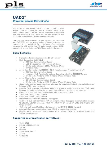
UAD2 +<br />
Universal Access Device2 plus<br />
The access to the whole choice of C166, XC166, XC2000,<br />
XE166, C166CBC, C166S V2, TriCore, PowerPC, ST30, STR7,<br />
ARM7, ARM9, ARM11, XScale, SH-2A derivatives is supported<br />
with the Universal Access Device 2+, the new all-in-one addon<br />
interface hardware for Universal Debug Engine.<br />
UAD2+ offers state-of-the-art hardware support for debugging<br />
via JTAG/OCDS and via a wide variety of target system access<br />
channels. It is optimized for High-Speed Communication<br />
between the UDE on the Host PC and a target system. UAD2+<br />
supports all access features of UDE in an optimized manner.<br />
Basic Features<br />
Standalone Communication device 17 x 14 x 5cm³<br />
Host Connection via USB 2.0<br />
o 480Mbps Communication Speed<br />
o USB 1.1 supported with reduced efficiency<br />
o Works under Windows 2000, Windows XP and<br />
Windows Vista<br />
or via Host Connection via IEEE1394-OHCI (also known as Firewire® or i.Link)<br />
o 400Mbps Communication Speed<br />
o Integrated Hub Function for optimal Operating with other IEEE1394Targets<br />
o Works under Windows 2000, Windows XP and Windows Vista<br />
or via Ethernet (in preparation)<br />
o 10/100Mbps Communication Speed<br />
o Works under Windows 2000, Windows XP and Windows Vista<br />
Galvanically isolated target interfaces minimize the negative effects of potential differences<br />
between UAD2+ and the target<br />
Build-in JTAG extender technology features a maximal cable length of the JTAG cable<br />
between the UAD2+ and the target up to 50 cm (1 meter and longer on request)<br />
JTAG port is provided via a dedicated pod with drivers and cables<br />
Serial Wire Debug (SWD) support<br />
Serial Wire Viewer (SWV) support<br />
Instrumentation Trace Macrocell (ITM) support<br />
CAN bus D-Sub male connector (CiA pin assignment) as debugging communication channel<br />
to C167CR, C164CI, XC161CJ, XC164CS, XC167CI or equivalent ST10 and TriCore CAN<br />
target systems<br />
On-board high-speed CAN bus interface driver for ISO-DIS 11898 standard<br />
Automatic firmware update via on-board Flash programming possible<br />
Flexible serial high-speed communication to an XC16x, C16x, ST10, ARM7, ARM9 and<br />
TriCore target system.<br />
Supported microcontroller derivatives<br />
<br />
<br />
<br />
<br />
<br />
<br />
<br />
C166, ST10<br />
XC166, XC2000, XE166<br />
TriCore<br />
PowerPC<br />
ARM7, ARM, ARM11<br />
XScale<br />
Cortex-M3<br />
I주I 임베디드시스템코리아
ASC Interface<br />
Universal Access Device 2+ provides a buffered asynchronous communication path between an<br />
external RS232 device controlled by the target system application and the ASC0 of the target<br />
system controller.<br />
In ASC-BSL/CAN, ASC-BSL/3Pin or ASC-BSL/SSC mode, after booting up the target system<br />
controller via ASC0 and transferring the monitor code the ASC0 channel will no longer be used by<br />
the debug communication and is therefore available for the application. With the buffered ASC0 of<br />
Universal Access Device 2+, the application's external RS232 device does not need to be manually<br />
reconnected - this is automatically done by Universal Access Device 2+.<br />
Additionally to the buffered ASC0 via RS232, an unbuffered TTL-level ASC0 is available. For this,<br />
no additional hardware (RS232 driver) at the target system is required - the signal lines TxD and<br />
RxD are directly connected to the corresponding controller pins.<br />
SSC Interface<br />
As no additional hardware is required, the maximum transmission speed of up to 5Mbps can be<br />
achieved.<br />
<br />
<br />
<br />
<br />
RS232/ASC0 for booting-up the target system. After downloading the monitor (
CAN communication channel may be used simultaneously for your application and for<br />
debugging because of the CAN bus node addressing.<br />
The CAN bus debugging monitor in the target system requires just 4kByte of code and<br />
128Bytes data memory; it can thus be easily integrated into nearly all types of target<br />
systems. 4 message identifier and 2 CAN module messages objects for host-to-target<br />
communication must be reserved. CAN bus timing is user-definable.<br />
The CAN debugging interface uses the on-chip CAN module of the C167CR, C167CS, C164CI,<br />
C161CS, C161JS, XC161, XC164, XC167, ST10R167, ST10R168 or TriCore TC1775, TC1130,<br />
TC1796 CAN derivatives or an external i82527 CAN bus controller for communication with<br />
debugger on the host PC. The Controller Area Network (CAN) bus and its associated protocol<br />
allows very efficient communication between a number of stations connected to the CAN bus.<br />
Accessing a number of stations simultaneously may be of great advantage when designing<br />
complex systems with a number of CAN nodes based on XC16x, C16x, ST10. Other software<br />
performance enhancing features of the CAN bus are: The CAN bus debug interface is an excellent<br />
solution allowing rapid access to the target system for software development, testing and on-site<br />
maintenance at all times.<br />
Special CAN Bus Target Monitor Features<br />
<br />
<br />
<br />
<br />
<br />
<br />
<br />
Target system monitors for XC16x, C16x, ST10 internal on-chip CAN module and external<br />
i82527 available.<br />
CAN bus ROM monitors for standard evaluation boards come with the Debugger Standard<br />
Package.<br />
User specific CAN bus monitors can be configured from the UDE-Mon Portable Monitor<br />
package. All components (sources, objects and libraries) are compatible with the available<br />
C16x / ST10 cross compilers.<br />
Standard and Extended Identifiers supported.<br />
CAN interrupt sharing between monitor and application using the On-Chip CAN module.<br />
Flash programming via CAN bus (internal FLASH and external FLASH-EPROMs AMD 29F<br />
xxx)<br />
ROM-less CAN debug monitors possible (ASC Bootstrap loader and CAN).<br />
CAN Bus Analyzer<br />
Independent intelligent subsystem enables continuous trace of CAN bus messages<br />
CAN bus observing capability, can also be used in conjunction with the CAN bus based<br />
debugger communication<br />
CAN bus stimulation - ideally suited for testing CAN applications !<br />
The Universal Access Device 2+ CAN Bus Monitoring tool is designed as a development aid for<br />
applications using the CAN bus and is not supposed to completely replace a CAN Analyzer.<br />
JTAG<br />
OnChip Debug Support (OCDS) - The New Debug Interface for Infineon C166CBC, C166S V2<br />
(XC16x) and TriCore Family Microcontrollers supported by Universal Debug Engine with Universal<br />
Access Device 2+ represents a new technology of debug support for the Infineon 16- and 32-bit<br />
microcontrollers. So far, OCDS functionality has been implemented into the newest C166CBC,<br />
C166S V2 derivatives and the new generation 32-bit µC-DSP TriCore architecture.<br />
Universal Access Device 2+ supports all of the essential OCDS features like:<br />
<br />
<br />
Standard 16 pin Infineon JTAG/OCDS L1 connector (2.5V - 3.3V I/O ring voltage) supports<br />
C166CBC, C166S V2 and TriCore JTAG debug communication channel up to 50 MHz shift<br />
clock - download rate up to 3,5 MByte/s<br />
Standard 20 pin ARM JTAG connector (2.5V - 3.3V I/O ring voltage) supports ARM7/ARM9<br />
JTAG debug communication channel up to 25 MHz shift clock - download rate up to 1<br />
MByte/s<br />
I주I 임베디드시스템코리아
Standard 14 pin PowerPC OnCE connector (2.5V - 3.3V I/O ring voltage) supports<br />
Freescale PowerPC OnCE debug communication channel up to 25 MHz shift clock<br />
Standard 16 pin PowerPC COP connector (2.5V - 3.3V I/O ring voltage) supports<br />
IBM/Motorola PowerPC COP debug communication channel up to 25 MHz shift clock<br />
Direct target system access for the host debugger via JTAG interface (IEEE1149.1)<br />
OnChip debug operations supports emulator-like additional debug functionality<br />
Hardware Code Breakpoints<br />
Read or Write Access Data Breakpoints<br />
Real-Time Trace Operand Access<br />
Using these debug features, no additional hard- or software resources in the target system are<br />
required. Therefore, when using the JTAG OCDS L1 port for the debugger all other interfaces of<br />
the microcontroller are available to the application with no limitations and the system is ready for<br />
debugging over its whole lifetime.<br />
Using JTAG OCDS L1 with Universal Debug Engine (UDE) and Universal Access Device 2+ gives the<br />
following major advantages:<br />
<br />
<br />
<br />
Download performance up to 25 times faster than the low-cost printer port solution!<br />
Dramatically speeds up the turn-around cycles of debug sessions, especially of larger<br />
applications (1++MByte).<br />
No resident target monitor in RAM or ROM required.<br />
Hardware breakpoints available for stepping through program code in ROM or OnChip-<br />
Flash/OTP.<br />
Furthermore, complex trigger conditions can be defined. Symbolic trigger conditions feature now<br />
enhanced definitions. With the Universal Access Device 2+, single-chip applications can now be<br />
debugged via JTAG OCDS L1 without costly in-circuit emulators.<br />
JTAG-Extender<br />
The UAD2+ is equipped with<br />
an active UAD-JTAG Extender<br />
per default and allows a<br />
maximal cable length of the<br />
JTAG cable between the<br />
UAD2+ and the target up to<br />
50 cm (1 meter and longer<br />
on request). The UAD-JTAG<br />
Extender provides a<br />
dedicated JTAG pod with<br />
drivers and cables. Supported<br />
JTAG Connectors:<br />
16 pin shroud male<br />
header - Infineon<br />
connector<br />
20 pin shroud male<br />
header - ARM<br />
connector<br />
Customer's<br />
connectors on<br />
request<br />
Cable length 50cm -<br />
longer cable length<br />
on request<br />
Support of open-drain<br />
RESET#<br />
Target MCU I/O voltage used for I/O operations<br />
LVDS technology for highest performance and signal integrity.<br />
I주I 임베디드시스템코리아
OCDS L2 Instruction Trace<br />
The OCDS L2 trace board is an add-on for the Universal Access Device 2+ and allows the recording<br />
of trace information of a running program on the TriCore in real-time.<br />
UAD OCDS L2 Trace Add-On Board<br />
The system is an optimized solution to support all the features of the Infineon OCDS L2 trace port<br />
functionality in the best manner.<br />
<br />
<br />
<br />
<br />
<br />
<br />
<br />
<br />
<br />
<br />
<br />
Trace ports supported up to 170 MHz<br />
1M Sample trace depth<br />
Timestamp resolution 1/ f CPU (i.e. 10ns at f CPU =100MHz)<br />
40bit time stamp range<br />
Support the full OCDS L1 functionality for providing the trigger events for the tracing unit<br />
Intelligent trace filter for optimal trace utilization<br />
TriCore and PCP trace<br />
Complete support of OCDS L1 trigger signals for trace control and visualization<br />
Additional 8 external trace lines to observe peripherals and external signals<br />
LVDS interface to external connector pod supports pods for 60 pin OCDS L2 High-Speed<br />
Connector (proposed by Infineon)<br />
Supported derivatives: TC1130, TC1765, TC1796, TC1910, TC1912, TC1920<br />
60 Pin OCDS L2 High-Speed Connector Pod<br />
Recommended by Infineon to support connection to OCDS L2 port of TriCore 1.3 systems<br />
(TC11IB, TC1910, TC1912, TC1920 and future derivatives)<br />
Connector system based on SAMTEC 60 pin high-speed connector QSH-030-01-F-D-A<br />
Prepared to use for<br />
systems up to<br />
150MHz system<br />
clock<br />
Supports 2.5 Volt<br />
to 3.6 Volt TriCore<br />
1.3 I/O ring<br />
voltage<br />
80 pin cable to<br />
trace base board<br />
using LVDS<br />
interface to ensure<br />
high trace signal<br />
quality<br />
UDE Support of OCDS<br />
L2 Trace Functions<br />
The complete utilization of<br />
trace functionality by 4<br />
setup modes:<br />
<br />
<br />
<br />
<br />
<br />
2 standard modes<br />
to allow easy<br />
access to standard trace tasks<br />
2 expert modes to allow full access to complex possibilities of trace system<br />
Full connection of trace setup to symbolic reference of source code<br />
Visualization of internal and external trace events<br />
Browse capability between trace output and C-language sources<br />
I주I 임베디드시스템코리아
ETM and ETB Trace for ARM7 and ARM9<br />
The ARM7 and ARM9 ETM trace board is an add-on for the Universal Access Device 2+ and allows<br />
the recording of trace information of a running program on the ARM derivatives in real-time.<br />
UAD ARM7 and ARM9 ETM Trace Add-On Board<br />
The system is an optimized solution to support all the features of the ARM ETM trace port<br />
functionality in the best manner.<br />
<br />
<br />
<br />
<br />
<br />
<br />
<br />
<br />
<br />
<br />
Trace ports supported up to 170 MHz, 4 or 8 bit width<br />
Halfrate Clock Mode supported<br />
1M Sample trace depth<br />
Timestamp resolution 1/ f CPU (i.e. 10ns at f CPU =100MHz)<br />
40bit time stamp range<br />
Support the full ETM functionality for providing the trigger events for the tracing unit<br />
Intelligent trace filter for optimal trace utilization<br />
Additional 8 external trace lines to observe peripherals and external signals<br />
LVDS interface to external connector pod supports pods for 38 pin ETM Mictor High-Speed<br />
Connector (proposed by ARM)<br />
Supported derivatives: LPC21xx, AT91RM9200<br />
38 Pin ARM7 and ARM9 Mictor<br />
High-Speed Connector Pod<br />
Recommended by ARM to<br />
support connection to ARM<br />
ETM<br />
Connector system based on<br />
Mictor 38 pin high-speed<br />
connector<br />
Prepared to use for systems<br />
up to 170MHz system clock<br />
Supports 2.5 Volt to 3.6 Volt<br />
I/O ring voltage<br />
80 pin cable to trace base<br />
board using LVDS interface<br />
to ensure high trace signal quality<br />
UDE Support of ETM Trace Functions<br />
The complete utilization of trace functionality by setup modes:<br />
<br />
<br />
<br />
<br />
1 standard mode to allow easy access to standard trace tasks<br />
Full connection of trace setup to symbolic reference of source code<br />
Visualization of internal and external trace events<br />
Browse capability between trace output and C-language sources<br />
UDE Support of ETB Trace Functions<br />
The Embedded Trace Buffer (ETB) extends the ETM unit of ARM derivatives by an embedded onchip<br />
circular trace buffer. This simplifies the adaptation of external trace units because the high<br />
speed trace signaling does not need to transfer to the external unit. The trace buffer is managed<br />
and read via the JTAG communication channel.<br />
<br />
Supported derivatives: LPC3000 derivatives<br />
I주I 임베디드시스템코리아
DAP Support for Infineons TriCore and XC2000<br />
The Device Access Port DAP, a new debug interface was established by Infineon for the AUDO<br />
Future,<br />
XC2000M, XE166M devices and other upcoming 16-bit and 32-bit-microcontrollers. The 2-wire or<br />
3-wire<br />
DAP allows debug communication with higher transmission rates than existing JTAG based<br />
communication channels. The new board connector is a 0.05 inch double row 10-pins microterminal<br />
with keying shroud, which saves board space on targets system side.<br />
UDE Support for DAP<br />
High-speed downloading via DAP is achieved by the communication devices UAD2 and UAD2+, the<br />
hardware addons of the Universal Debug Engine.<br />
<br />
<br />
<br />
<br />
<br />
DAP communication frequency @ 50 MHz<br />
Transfer rate up to 3,5 MByte/s ( with TC1797 AUDO Future)<br />
2-wire/pin and 3-wire/pin DAP mode supported<br />
Prepared for single-wire/pin DAP mode<br />
LED for power indicating<br />
UAD DAP Extender with LVDS<br />
The UAD2+ with DAP Extender uses the LVDS technology and a galvanically isolated interface for<br />
highest<br />
performance and signal integrity of the DAP interface. It allows interface cable length of up to 2<br />
meters<br />
SWD Support for Cortex<br />
The Serial Wire Debug (SWD) interface or Serial Wire Debug Port (SW-DP) is one of the features of<br />
the debug and trace technology ARM CoreSight. First implementations of SWD are realized in the<br />
derivatives of the Cortex-M3 core Stellaris of Luminary Micro (now Texas Instruments) and in the<br />
derivatives of the STM32 family by STMicroelectronics. The known JTAG Debug Port (JTAG-DP) is<br />
supported furthermore. Both debug ports, the SWD and the alternative JTAG debug port can be<br />
combined to the Serial Wire JTAG Debug Port (SWJ-DP), the CoreSight standard port.<br />
When using SWD, the TDO signal can provide trace event messages via the Serial Wire Output<br />
(SWO). This behaviour can be used by the Serial Wire Viewer (SWV) to output system events via a<br />
single pin:<br />
<br />
<br />
<br />
Instrumentation trace ITM (printf-like Debugging)<br />
Watchpoint Trace DWT, Instruction Pointer Trace<br />
Event Trace (Interrupts)<br />
UDE Support for SWD<br />
Target connection via SWD is achieved by the communication devices UAD2 and UAD2+, the<br />
hardware add-ons of the Universal Debug Engine and the additional UAD2 SWD adapter.<br />
UAD SWD Extender with LVDS<br />
The UAD2+ in touch with the Extender and the SWD adaptor uses the LVDS technology and a<br />
galvanically isolated interface for highest performance and signal integrity of the SWD interface. It<br />
allows interface cable length of up to 2 meters.<br />
I주I 임베디드시스템코리아
Electrostatic Precautions<br />
Electrostatic Discharge (ESD) can damage a sensitive electronic component !<br />
Under several conditions static electricity and ground potential differences<br />
between the Access Device and the user's target hardware can build up high<br />
voltages - over 10000 Volts (10 kV) in some cases. The electrostatic discharge<br />
of this build-up voltage results in fast high current waveforms and fast<br />
magnetic (H-field) or electrostatic (E-field) disturbances.<br />
The discharge into the electronic components and circuitry can damage or destroy hardware<br />
components, resulting in failures and reduced reliability. Because of the non-hot-pluggable 3.3<br />
Volts / 5 Volts - TTL properties of the JTAG and the 3Pin/Serial connectors, these ports are<br />
endangered especially. The maximum voltage on these pins may not exceeded 5.5 Volts against<br />
the UAD’s ground, especially in the case that the ground planes are not connected first.<br />
To protect your hardware against damage from static electricity and ground potential discharge,<br />
you should follow some basic precautions:<br />
1. Before you change any cable connections from the Access Device, please remove the<br />
power from the Access Device and your target system.<br />
2. Please ensure that the static electricity and ground potentials between the Access Device,<br />
the host PC and the target hardware are balanced. If there is a danger of high potential<br />
differences, you must connect the Access Device, the host PC and the target hardware to<br />
the same ground domain via a low resistance connection.<br />
3. Establish the target connection and power on the systems.<br />
In all cases, the following rule must be attended:<br />
The first connection between the devices must be done via the ground !<br />
Solution<br />
All Universal Access Devices are equipped with a ground socket on the front side. Please use this<br />
ground socket for discharging the static electricity and balancing ground potentials between the<br />
Universal Access Device, the host PC and the target hardware BEFORE you connect the target<br />
hardware to the Access Device.<br />
The UAD2+ contains protection function already. Please note, that these protection functions<br />
DOES NOT suspend the precautions described above.<br />
I주I 임베디드시스템코리아