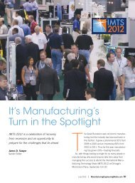
The RAPID 2013 Conference & Exposition Directory - Society of ...
The RAPID 2013 Conference & Exposition Directory - Society of ...
The RAPID 2013 Conference & Exposition Directory - Society of ...

You also want an ePaper? Increase the reach of your titles
YUMPU automatically turns print PDFs into web optimized ePapers that Google loves.
Direct Write Printed Materials & Electronics<br />
10 am–3:25 pm<br />
<strong>The</strong> technology is advancing beyond research and development.<br />
Hear about applications <strong>of</strong> additive manufacturing for printed<br />
electronics and other related products.<br />
10–10:25 am<br />
Printed Optics: Interactive Objects<br />
and Devices using Optically Clear<br />
Materials and Embedded Components<br />
Eric Brockmeyer, Lab Associate, Disney Research Pittsburgh<br />
Karl D.D. Willis, PhD, Principal Research Engineer, Autodesk<br />
Additive manufacturing technology allows us to create unique,<br />
personalized products for consumers and experiences for guests<br />
<strong>of</strong> Disney parks, hotels, and resorts. We believe that the next<br />
generation <strong>of</strong> these products will enable us to integrate interactive<br />
display, sensing, and illumination elements. Our research using<br />
jetted additive manufacturing explores novel techniques for<br />
creating optical components and a variety <strong>of</strong> applications.<br />
Our library <strong>of</strong> optical components includes: optical fiber-like<br />
‘light pipes,’ internal light reflectors using enclosed air pockets,<br />
micro lens arrays, and embedded opto-electronic components.<br />
We used an Objet Connex 260 and have developed techniques<br />
for routing light pipes, building overhanging geometry without<br />
support, and smoothing/finishing optical components while<br />
still in the machine. <strong>The</strong>se techniques are used in a range <strong>of</strong><br />
applications to guide light from displays onto arbitrarily shaped<br />
objects, to reflect light in 3D displays and lighting elements, and<br />
to embed opto-electronic components for touch sensing. We<br />
believe additive manufacturing <strong>of</strong> optical components will enable<br />
unique, personalized interactive objects for consumer products<br />
and experiences <strong>of</strong> the future.<br />
10:30–10:55 am<br />
Complete Electrical Assemblies Made with<br />
Additive Manufacturing: Medical Applications<br />
Mario Urdaneta, PhD, Staff Scientist/Engineer,<br />
Weinberg Medical Physics<br />
Additive manufacturing typically uses a single material type,<br />
whether it is plastic, metal, or ceramic, to make an entire part.<br />
Rapid prototyping parts that combine different materials (e.g.,<br />
conductors and insulators as in an electrical motor) in a single<br />
process are not yet an option. We have developed methods to<br />
make rapid prototype parts that combine electrical conductors<br />
and insulators for making MRI gradient and RF coils. <strong>The</strong> parts<br />
include wires, insulation, cooling lines, and supporting structures.<br />
Our primary motivation is rapid prototyping MRI wires (i.e., Litz-like<br />
wires), which must be woven in sophisticated patterns to reduce<br />
proximity and skin-effects that produce losses at high frequencies<br />
and currents (patent pending). Our additive manufacturing<br />
approach will bypass the months-long and nearly-artisanal process<br />
<strong>of</strong> winding a Litz wire. Using additive manufacturing we can make<br />
wires with very tight turns, leading to coils that take less space<br />
and enable the design <strong>of</strong> MRIs with non-traditional shapes (e.g.,<br />
dental MRI). We anticipate that eventually additive manufacturing<br />
<strong>of</strong> conductors and insulating structures will revolutionize the<br />
manufacturing <strong>of</strong> many electromagnetic components, especially in<br />
high-frequency applications (e.g., hybrid cars).<br />
11–11:25 am<br />
Fabrication and Characterization <strong>of</strong> 3D Printed<br />
Compliant Tactile Sensors<br />
Jae-Won Choi, Assistant Pr<strong>of</strong>essor, University <strong>of</strong> Akron<br />
Morteza Vatani, PhD Candidate, University <strong>of</strong> Akron<br />
Erik Engeberg, Assistant Pr<strong>of</strong>essor, University <strong>of</strong> Akron<br />
Additive manufacturing technology with a direct-write<br />
conductive material is one promising approach to produce<br />
compliant tactile sensors. In this work, a multi-layer compliant<br />
tactile sensor was developed using a hybrid manufacturing<br />
process with an existing projection micro-stereolithography<br />
and micro-dispensing process. <strong>The</strong> sensor was designed to<br />
detect changes in resistance as it is deformed. A compliant<br />
skin structure was built layer-by-layer using a stretchable<br />
photopolymer in the micro-stereolithography system to cover<br />
the conductive elements. <strong>The</strong>se sensing elements were created<br />
within the skin material by the micro-dispensing <strong>of</strong> a compliant<br />
conductive material during the micro-stereolithography process.<br />
<strong>The</strong> fabricated tactile sensor consists <strong>of</strong> two layers <strong>of</strong> sensing<br />
elements within the skin structure; there are eight stretchable<br />
straight wires in each layer. <strong>The</strong> wires in the second layer<br />
were orthogonally placed atop the first layer so that the sensor<br />
can detect various external forces/motions in two dimensions.<br />
To introduce conductivity, carbon nanotubes were dispersed<br />
in the stretchable photopolymer. <strong>The</strong> fabricated sensor was<br />
6/<strong>2013</strong> – <strong>RAPID</strong> 51