Henkel Semiconductor Solutions
Henkel Semiconductor Solutions
Henkel Semiconductor Solutions

Create successful ePaper yourself
Turn your PDF publications into a flip-book with our unique Google optimized e-Paper software.
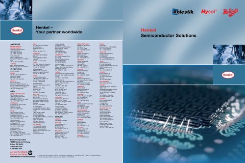
<strong>Henkel</strong> –<br />
Your partner worldwide<br />
<strong>Henkel</strong><br />
<strong>Semiconductor</strong> <strong>Solutions</strong><br />
AMERICAS<br />
HEADQUARTERS:<br />
UNITED STATES<br />
15350 Barranca Parkway<br />
Irvine, CA 92618<br />
Tel: 1-949-789-2500<br />
Tel: 1-800-562-8483<br />
<strong>Henkel</strong> Ablestik<br />
20021 Susana Road<br />
Rancho Dominguez, CA 90221<br />
USA<br />
Tel: +1-310-764-4600<br />
CANADA<br />
2225 Meadowpine Blvd.<br />
Mississauga, Ontario L5N 7P2<br />
Tel: 1-905-814-6511<br />
Tel: 1-800-263-5043<br />
(within Canada)<br />
BRAZIL<br />
Av. Prof. Vernon Krieble, 91<br />
06690-250 Itapevi,<br />
Sao Paulo, Brazil<br />
Tel: +55 11 41 43 7000<br />
Mexico<br />
<strong>Henkel</strong> Mexicana<br />
Boulevard Magnocentro No. 8<br />
Centro Urbano Interlomas, 52760<br />
Huixquilucan, Edo. de Mexico<br />
Tel: +52 55 3300 3000<br />
ASIA<br />
HEADQUARTERS: ASIA<br />
928 Zhangheng Road,<br />
Zhangjiang Hi-Tech Park,<br />
Pudong New District,<br />
Shanghai, 201203, P. R. China<br />
Tel: +86 21 2891 8000<br />
AUSTRALIA<br />
Unit 29 38-46 South Street,<br />
Rydalmere 2216,<br />
Sydney, Australia<br />
Tel: +61 2 8844 4700<br />
CHINA<br />
928 Zhangheng Road,<br />
Zhangjiang Hi-Tech Park,<br />
Pudong New District,<br />
Shanghai, 201203, P. R. China<br />
Tel: +86 21 2891 8000<br />
<strong>Henkel</strong> Ablestik<br />
332 Mei Gui South Road,<br />
Waigaoqiao FTZ<br />
Shanghai 200131 China<br />
Tel: +86 21 3898 4800<br />
<strong>Henkel</strong> Ablestik<br />
Unit 1601-6 Level 16<br />
Metroplaza Tower 1<br />
No. 223 Hing Fong Road<br />
Kwai Fong NT, Hong Kong, China<br />
Tel: +852 2968-2977<br />
<strong>Henkel</strong> Corporation<br />
15350 Barranca Parkway<br />
Irvine, CA 92618<br />
1-949-789-2500<br />
1-800-562-8483<br />
Across the Board,<br />
Around the Globe.<br />
www.henkel.com/electronics<br />
INDIA<br />
No.1, Airport Service Road,<br />
Domlur Layout,<br />
Bangalore-560 071,<br />
India<br />
Tel: +91 80 2535 7771<br />
INDONESIA<br />
Jalan Raya Jakarta Bogor<br />
KM31.2,<br />
Cimanggis Depok 16953,<br />
Indonesia<br />
Tel: +62 21 8775 2196<br />
JAPAN<br />
27-7 Shin Isogo-cho, Isogo-ku,<br />
Yokohama, Japan 235-0017<br />
Tel: +81 45 758 1800<br />
<strong>Henkel</strong> Ablestik<br />
100 Kaneda, Kanagawa<br />
Atsugi-shi, Japan 243-0807<br />
Tel: +81 46 294 2511<br />
KOREA<br />
1st Floor, Mapo-tower,<br />
418, Mapo-dong, Mapo-gu,<br />
121-734 Seoul, Korea<br />
Tel: +82 2 3279 1730<br />
<strong>Henkel</strong> Ablestik<br />
6th Floor, Dae Ryung Techno<br />
Town II<br />
569-21 Gasan-dong,<br />
Kumchun-gu,<br />
Seoul, Korea<br />
Tel: +822 6675-8000<br />
MALAYSIA<br />
Lot 973, Jalan Kampung<br />
Baru Hicom,<br />
Persiaran Tengku Ampuan,<br />
Lion Industrial Park, Sek 26,<br />
Shah Alam, 40400 Selangor,<br />
Malaysia<br />
Tel: +60 3 5192 6200<br />
<strong>Henkel</strong> Ablestik<br />
c/o NSC (M) Sdn Bhd., 88K-2<br />
Jalan Tun Dr Awang, Sri Bukit<br />
Jambul<br />
11900 Bayan Lepas,<br />
Penang, Malaysia<br />
Tel: +60 4-6435244<br />
c/o NSC (M) Sdn Bhd., Lot 8 & 10<br />
Jalan Tukul 16/5,<br />
40000 Shah Alam,<br />
Selangor, Malaysia<br />
Tel: +60 3-55191105<br />
PHILIPPINES<br />
21/F, Asia Star Building,<br />
2402-2404 Asean Drive,<br />
Filinvest Corporate City,<br />
Alabang, Muntinlupa City 1781,<br />
Philippines<br />
Tel: +632 859 3100<br />
<strong>Henkel</strong> Ablestik<br />
2 Perfector Drive,<br />
Sta Maria Industrial Estate<br />
Bagumbayan, Taguig,<br />
Metro Manila<br />
1600 Philippines<br />
Tel: +632 837-5898<br />
SINGAPORE<br />
401, Commonwealth Drive<br />
#03-01/02,<br />
Haw Par Techno Centre,<br />
Singapore 149598<br />
Tel: +65 6266 0100<br />
<strong>Henkel</strong> Ablestik<br />
Block 11, Kallang Place #07-10<br />
Kallang Basin Industrial Estate<br />
Singapore 339155<br />
Tel: +65 6297-1332<br />
TAIWAN<br />
10/F, No.866, ZhongZheng Road,<br />
ZhongHe City, Taipei County 235,<br />
Taiwan<br />
Tel: +886 2 2227 1988<br />
<strong>Henkel</strong> Accurus<br />
508-51, Wen-sien Road, Section 1<br />
Jen-der, Tainan County<br />
Taiwan 717<br />
Tel: +886 6 366 1288<br />
<strong>Henkel</strong> Ablestik<br />
B-5F, No. 356 Sec 2<br />
Ching Nien Road<br />
Feng Shan City,<br />
Kaoshiung, Taiwan<br />
Tel: +886 7-776-2313<br />
THAILAND<br />
Centralworld, 35th Floor,<br />
999/9 Rama 1 Road,<br />
Patumwan, Bangkok, 10330,<br />
Thailand<br />
Tel: +66 2 209 8000<br />
<strong>Henkel</strong> Ablestik<br />
c/o NSC,40/14 Moo<br />
12 Bangna Trad Road<br />
Bangkaew, Bangplee,<br />
Samutprakarn 10540 Thailand<br />
Tel: +662 3120530-45<br />
EUROPE<br />
AUSTRIA<br />
See <strong>Henkel</strong> Germany<br />
BELGIUM<br />
<strong>Henkel</strong> Belgium N.V.<br />
Havenlaan 16<br />
B-1080 Brussel<br />
Tel: +32-(0)2-42125 55<br />
BULGARIA<br />
<strong>Henkel</strong> Bulgaria E.O.O.D.<br />
Business Park Sofia<br />
Block 2, 4th floor<br />
BG-1715 Sofia<br />
Tel: +359 2 9151010<br />
CZECH REPUBLIC<br />
<strong>Henkel</strong> CR, spol. s r.o.<br />
U Pruhonu 10<br />
CZ-170 04 Praha 7<br />
Tel: +420 2 20101401<br />
CROATIA<br />
<strong>Henkel</strong> Croatia d.o.o.<br />
Budmanijeva 1<br />
HR-10000 Zagreb<br />
Tel. +85 1 6008-161<br />
DENMARK<br />
<strong>Henkel</strong> Norden AB,<br />
Copenhagen<br />
Horskaetten 3<br />
DK-2630 Taastrup<br />
Tel: +45 43 30 13 01<br />
FINLAND<br />
<strong>Henkel</strong> Norden Oy<br />
Ayritie 12 a<br />
01510 Vantaa<br />
Tel: +358 020 122 311<br />
FRANCE<br />
<strong>Henkel</strong> Loctite ® France<br />
10, Avenue Eugene Gazeau<br />
BP 40090<br />
F-60304 Senlis-Cedex<br />
Tel: +33 0344 216600<br />
GERMANY<br />
<strong>Henkel</strong> KGaA<br />
Gutenbergstrasse 3<br />
85748 Garching<br />
Tel: +49 (0)89 92680<br />
HUNGARY<br />
<strong>Henkel</strong> Magyarorszag Kft.<br />
H-1113 Budapest<br />
David Ferenc u. 6<br />
Tel: +36 30 9192884<br />
ITALY<br />
<strong>Henkel</strong> Loctite ® Adesivi S.r.l.<br />
Via Talete 56<br />
20047 Brugherio (MI)<br />
Tel: +39 039 21251<br />
NETHERLANDS<br />
<strong>Henkel</strong> Nederland B.V.<br />
<strong>Henkel</strong> Technologies<br />
Postbus 2100<br />
3430 CM Nieuwegein<br />
Tel: +31 030 607 38 50<br />
NORWAY<br />
Postboks:<br />
6405 Etterstad<br />
0604 Oslo<br />
Tel: +47 23 37 15 20<br />
POLAND<br />
<strong>Henkel</strong> Polska S.A.<br />
Domaniewska 41<br />
PL-02-672 Warszawa<br />
Tel: +48 22 5656200<br />
ROMANIA<br />
See <strong>Henkel</strong> Hungary<br />
® and designate trademarks of <strong>Henkel</strong> Corporation or its Affiliates. ® = registered in the U.S. Patent and Trademark Office.<br />
© <strong>Henkel</strong> Corporation, 2008. All rights reserved. 5204/LT-5013 (6/2008)<br />
RUSSIA<br />
RUSHENK<br />
Bakhrushina Ul., 32, Building 1<br />
RU-113054 Moscow<br />
Tel: +7 095 7452318<br />
SLOVAKIA<br />
<strong>Henkel</strong> Slovensko s.r.o.<br />
Zahradnicka 91<br />
P.O. Box 66<br />
SK-821 08 BRATISLAVA<br />
Tel: +421 2 50246402, 111<br />
SPAIN<br />
<strong>Henkel</strong> Iberica, S.A.<br />
Pol. Ind. Alparrache<br />
Camino de Villaviciosa, 18 y 20<br />
28600 Navalcarnero,<br />
Madrid<br />
Tel: +34 91 860 90 00<br />
SWEDEN<br />
<strong>Henkel</strong> Norden AB<br />
P.O. Box 120 80,<br />
SE-102 22 Stockholm,<br />
Sweden<br />
Tel: +46 863443800<br />
SWITZERLAND<br />
See <strong>Henkel</strong> Germany<br />
TURKEY<br />
Türk <strong>Henkel</strong> Kimya Sanayi ve<br />
Ticaret A.S.<br />
Kayisdagi CadKaraman Ciftligi<br />
YoluKar Plaza D Blok<br />
34752 Icerenköy - Istanbul,<br />
Turkey<br />
Tel: 0090 216 579 4000<br />
Fax: 0090 216 579 4092<br />
UKRAINE<br />
POW <strong>Henkel</strong> Ukraine<br />
Silver Centre<br />
4, Lepse Blvd.<br />
UA-03067 Kiev<br />
Tel: +38 044 20145 77<br />
Ireland and UK<br />
<strong>Henkel</strong> Loctite ®<br />
Adhesives Limited<br />
Technologies House<br />
Wood Lane End,<br />
Hemel Hempstead<br />
Hertfordshire HP2 4RQ<br />
Technologies House<br />
Tel: +44 (0)1442 278000<br />
<strong>Henkel</strong> Ablestik<br />
Station Road, Linton<br />
Cambridge CB1 6NW<br />
United Kingdom<br />
Tel: +44 1-223-893-771
Worldwide Manufacturing<br />
& Organization<br />
Electronics Group of <strong>Henkel</strong><br />
Irvine, California<br />
Rancho Dominguez, California<br />
Port Huron, Michigan<br />
Dublin, Ireland<br />
Linton, UK<br />
Hemel Hempstead, UK<br />
Yantai,China<br />
Billerica,<br />
Massachusetts<br />
Canton, Massachusetts<br />
Olean, New York<br />
Salisbury, North Carolina<br />
Hokkaido,<br />
Japan<br />
Isogo, Japan<br />
Atsugi, Japan<br />
Kakogawa, Japan<br />
San Diego,<br />
California<br />
Ontario,<br />
California<br />
Ecatepec de Morelos,<br />
Mexico<br />
Westerlo,<br />
Belgium<br />
Scheemda,<br />
Netherlands<br />
Lianyungang,<br />
China<br />
Shanghai, China<br />
Ipoh, Malaysia<br />
Seoul, Korea<br />
Tainan, Taiwan<br />
Sao Paulo, Brazil<br />
Kuala Lumpur, Malaysia<br />
Headquarters/Product Development<br />
Product Development/Manufacturing<br />
Product Development<br />
Manufacturing<br />
Headquarters/Product Development<br />
Product Development/Manufacturing<br />
Product Development Corporate Profile – <strong>Henkel</strong> Corporation<br />
Manufacturing<br />
<strong>Henkel</strong> is the world’s leading and most progressive provider of<br />
Across the Board,<br />
qualified, compatible material sets for semiconductor packaging,<br />
Around the Globe.<br />
printed circuit board (PCB) assembly and advanced soldering<br />
www.henkel.com/electronics<br />
solutions. As the only materials developer and formulator with<br />
vast technical expertise for all materials required for package<br />
production and assembly, <strong>Henkel</strong> is uniquely positioned to<br />
deliver world-class materials products, process expertise and<br />
total solutions across the board to enable tomorrow’s<br />
electronic industry.
Contents<br />
<strong>Semiconductor</strong> Market <strong>Solutions</strong><br />
Discrete Components .......................... 5<br />
Quad Flat Pack (QFP). .......................... 9<br />
Quad Flat No-Lead (QFN) ...................... 11<br />
Dynamic Random Access Memory (DRAM) ....... 14<br />
Ball Grid Array/Chip Scale Package (BGA/CSP). ... 15<br />
Flash Memory ................................ 19<br />
<strong>Semiconductor</strong> Materials<br />
Die Attach Adhesives. ......................... 21<br />
<strong>Semiconductor</strong> Underfills ...................... 26<br />
Hysol ® <strong>Semiconductor</strong> Encapsulants. ............ 29<br />
Hysol ® Thermal Compression Materials .......... 31<br />
Hysol ® Coating Powders ....................... 33<br />
Hysol ® Electronic Molding Compounds ........... 34<br />
Hysol ® and Hysol ® Huawei <strong>Semiconductor</strong><br />
Molding Compounds .......................... 36<br />
Multicore ® Accurus Solder Spheres ............. 44<br />
Periodic Table of Elements ..................... 48
Material <strong>Solutions</strong> for<br />
Electronic Packaging<br />
and Assembly<br />
<strong>Semiconductor</strong> Materials<br />
PCB Assembly Materials<br />
Flat Panel<br />
Display<br />
Materials<br />
Die Attach<br />
Adhesives<br />
<strong>Semiconductor</strong><br />
Underfills<br />
<strong>Semiconductor</strong><br />
Encapsulants<br />
Thermal<br />
Compression<br />
Materials<br />
Coating Powders<br />
Electronic Molding<br />
Compounds<br />
<strong>Semiconductor</strong><br />
Molding<br />
Compounds<br />
Solder and Flux<br />
Materials<br />
Solder and Flux<br />
Materials<br />
Chip on Board<br />
Encapsulant Materials<br />
Board Level<br />
Underfills<br />
Thermal Management<br />
Materials<br />
Electrically<br />
Conductive Adhesives<br />
Surface Mount<br />
Adhesives<br />
Circuit Board<br />
Protection <strong>Solutions</strong><br />
Adhesives<br />
Cleaners, Developers<br />
and Strippers<br />
2<br />
Please see LT-5012<br />
for PCB Assembly <strong>Solutions</strong> Guide<br />
Please see LT-5014 for<br />
Flat Panel Display <strong>Solutions</strong> Guide<br />
3
<strong>Semiconductor</strong><br />
Market <strong>Solutions</strong><br />
<strong>Semiconductor</strong><br />
Market <strong>Solutions</strong><br />
Discrete components<br />
Discrete Components<br />
Die Attach Adhesives<br />
Electronic Molding<br />
Compounds<br />
Encapsulants<br />
Molding<br />
Compounds<br />
Conductive<br />
Non-Conductive<br />
GR2220<br />
FP0087<br />
Green<br />
Non-Green<br />
DA100 (Solder)<br />
QMI536HT<br />
GR2310<br />
GR15F-A<br />
KL1000-3LX<br />
QMI529HT<br />
QMI547<br />
GR2710<br />
GR15F-1<br />
KL1000-4T<br />
2600AT<br />
GR2811<br />
GR360A-F8<br />
KL5000-HT<br />
8008HT (WBC)<br />
MG40FS<br />
GR750<br />
MG15F<br />
FS849-TI<br />
GR750-SC<br />
GR750HT-25<br />
KLG100<br />
KLG200<br />
die attach Adhesives: CONDUCTIVE<br />
Product<br />
QMI529HT<br />
Description<br />
For component or die attach where very high electrical and thermal<br />
conductivity is required. Suitable for high heat dissipation devices<br />
and solder replacement applications.<br />
Finish<br />
(Cu, Ag, Au)<br />
MRT<br />
Electrical<br />
Conductivity<br />
Dispensability<br />
Ag, Au L1 - 260 4 x 10 -5 Fair<br />
Cure<br />
Schedule<br />
≥ 60 sec @ 185°C<br />
(SkipCure)<br />
30 min @ 185°C (Oven)<br />
Thermal<br />
Conductivity,<br />
W/mK<br />
7.0<br />
2600AT<br />
High thermal conductivity adhesive for thermal<br />
management applications.<br />
Cu, Ag, Au L3 - 260 5 x 10 -5 Fair<br />
30 min ramp to 200°C<br />
+ 15 min @ 200°C<br />
20<br />
8008HT (WBC)<br />
High electrical and thermal conductivity die attach. Excellent<br />
temperature resistance.<br />
Ag, Cu, Au L1 - 260 6 x 10 -5 NA<br />
B-stage +<br />
20 sec @ 280°C<br />
11<br />
Across the Board,<br />
Around the Globe.<br />
www.henkel.com/electronics<br />
<br />
FS849-TI High thermal conductivity adhesive with low electrical resistance. Ag, Au L2 - 260 2 x 10 -5 Good<br />
15 min ramp to 175°C<br />
+ 30 min @ 175C<br />
7.8<br />
4<br />
5
<strong>Semiconductor</strong><br />
Market <strong>Solutions</strong><br />
<strong>Semiconductor</strong><br />
Market <strong>Solutions</strong><br />
Discrete COMPONENTS<br />
Die Attach: Conductive SOLDER<br />
MOLDING COMPOUNDs: GREEN<br />
Discrete COMPONENTS<br />
Product Description Application<br />
Viscosity,<br />
cPs<br />
ALLOY Reflow Cleanability<br />
Void<br />
Levels<br />
IPC/J-std-004<br />
Classification<br />
Product Description Voltage rating<br />
Ionic<br />
Permitivity,<br />
ROOM TEMP<br />
Ionic<br />
Permitivity,<br />
150°C<br />
MSL<br />
GREEN<br />
Spiral<br />
Flow, cm<br />
CTE a1,<br />
ppm/°C<br />
Tg, °C<br />
DA100<br />
(Solder)<br />
Flux designed for solder die attach paste applications. Dispensing 250,000 High Pb Forming Gas Excellent Very Low ROL0<br />
GR15F-A<br />
Very high Tg, low stress, green semiconductor grade epoxy molding<br />
compound designed specifically for high voltage applications. It also<br />
boasts superior performance for high temperature power applications due<br />
to its high Tg and use of advanced Sigma Technology.<br />
>900V discrete,<br />
>400V IC<br />
3.7 5.5 L1/260°C Y 80 10 185<br />
die attach ADHESIVES: NOn-Conductive<br />
Product<br />
QMI536HT<br />
Description<br />
High thermal version of QMI536, ideal for mixed stacked<br />
die applications. Non-die damaging filler.<br />
Finish<br />
(Cu, Ag, Au)<br />
MRT<br />
Electrical<br />
Conductivity<br />
Dispensability<br />
Ag, Au L3 - 260 1 x 10 13 Excellent<br />
QMI547 Non-conductive paste for leadframe applications. Au, Ag, Cu L3 - 260 1 x 10 13 Excellent<br />
Cure<br />
schedule<br />
≥8 sec @ 150°C<br />
(SkipCure)<br />
15 min @ 150°C (Oven)<br />
≥8 sec @ 150°C<br />
(SkipCure)<br />
15 min @ 150°C (Oven)<br />
Thermal<br />
Conductivity,<br />
W/mK<br />
0.9<br />
0.3<br />
GR15F-1<br />
Product<br />
GR750<br />
Green anhydride cured molding compound contains spherical filler and<br />
is designed for high voltage applications. This product has excellent<br />
moldability performance with high yield rates.<br />
Description<br />
GR750 has alumina fillers and delivers a high thermal conductive<br />
solution for TO-220F/3PF’s thermal requirements. GR750’s low<br />
moisture absorption and low thermal expansion is suitable for stress<br />
sensitive devices. GR750 is a green solution.<br />
>900V discrete,<br />
>400V IC<br />
Thermal<br />
Conductivity,<br />
W/mK<br />
3.7 5.8 L1/235°C Y 80 18 210<br />
GREEN<br />
Spiral<br />
Flow, cm<br />
Hot Plate<br />
Gel Time,<br />
sec<br />
2.1 W/mK Y 65 30<br />
Filler<br />
type<br />
Alumina/<br />
Crystalline<br />
CTE a1,<br />
ppm/°C<br />
Tg, °C<br />
23 160<br />
Electronic molding compounds<br />
Product<br />
GR2220<br />
Description<br />
Black/conventional molding of<br />
MnO caps.<br />
Conventional<br />
Mold<br />
Spiral<br />
Flow<br />
in, @ 177°C<br />
Tg, °C<br />
CTE a1,<br />
ppm/°C<br />
CTE a2,<br />
ppm/°C<br />
Cure Time<br />
@ 177°C<br />
Flexural<br />
Strength,<br />
psi<br />
Flexural<br />
Modulus,<br />
psi<br />
Laser<br />
Markable<br />
Conv 40 162 13 60 30 - 45 sec 18,500 2.4 x 10 6 N<br />
GR750-SC<br />
GR750HT-25<br />
GR750-SC is a high thermal conductivity molding compound using<br />
fully rounded spherical crystalline fillers designed to improve thermal<br />
management for semiconductor devices. It exhibits high adhesion to<br />
copper and copper alloys. This material is specifically recommended for<br />
isolated Power Transistors.<br />
GR750HT-25 is a high thermal conductivity molding compound<br />
using fully alumina fillers designed to improve thermal management for<br />
semiconductor devices. It exhibits high adhesion to copper and copper<br />
alloys. This material is specifically recommended for isolated Power<br />
Transistors, which require high heat dissipation.<br />
2.1 W/mK Y 45 26 Crystalline 20 155<br />
2.7 W/mK Y 55 34 Alumina 15 140<br />
GR2310<br />
Gold/non-halogenated molding powder,<br />
tantalum and ceramic capacitors,<br />
leaded or surface-mounted sensors.<br />
Auto/Conv 27 166 22 75 30 - 45 sec 20,500 2.1 x 10 6 Y<br />
Product<br />
Description<br />
Thermal<br />
Conductivity,<br />
W/mK<br />
MSL<br />
GREEN<br />
Spiral<br />
Flow,<br />
cm<br />
Hot Plate<br />
Gel Time,<br />
sec<br />
FILLER<br />
TYPE<br />
CTE a1,<br />
ppm/°C<br />
Tg, °C<br />
GR2710<br />
Gold/low stress/non-flame retarded<br />
molding powder, tantalum and ceramic<br />
capacitors, leaded or surfacemounted<br />
sensors.<br />
Auto/Conv 35 161 13 45 45 - 60 sec 19,000 2.6 x 10 6 Y<br />
GR360A-F8<br />
Green mold compound with 1/8" flammability rating suitable for bridge,<br />
axial and TO packages. GR360A-F8 offers good moldability with lowest<br />
cost of ownership.<br />
0.9 W/mK L3/260°C Y 65 35 Fused 16 165<br />
GR2811<br />
MG40FS<br />
ENCAPSULANTS<br />
Gold/thin wall-crack resistant, low<br />
stress, fast cycle time.<br />
Black/conventional molding of SMD<br />
and SIP networks. Gold version<br />
MG40F-0526 available.<br />
Auto/Conv 34 162 13 45 30 - 45 sec 20,000 2.9 x 10 6 Y<br />
Conv 35 160 20 75 60 - 90 sec 19,000 2.4 x 10 6 N<br />
KLG100<br />
KLG200<br />
Green mold compound with 1/4" flammability rating suitable for bridge,<br />
axial and TO packages. Offers superior moldability with lowest cost<br />
of ownership.<br />
Green mold compound with 1/4" flammability rating suitable for bridge,<br />
axial and TO packages. KLG200 offers superior moldability with lowest<br />
cost of ownership.<br />
0.9 W/m.K L3/260°C Y 80 23 Crystalline 22 165<br />
0.9 W/mK L3/260°C Y 80 23<br />
Crystalline/<br />
Fused<br />
22 165<br />
Product<br />
Description<br />
Recommended<br />
Cure<br />
Flow Speed<br />
Viscosity<br />
25°C, cPs<br />
Tg, °C CTE a1, ppm/°C % Filler<br />
FP0087<br />
Low stress fill for potting automated sensor and diodes,<br />
high Tg.<br />
1 hr @ 125°C<br />
+ 1 hr @ 180°C<br />
High 20,000 175 18 76<br />
6<br />
7
<strong>Semiconductor</strong><br />
Market <strong>Solutions</strong><br />
<strong>Semiconductor</strong><br />
Market <strong>Solutions</strong><br />
Discrete components<br />
QFP<br />
Molding Compounds: Non-Green<br />
Product<br />
Description<br />
Thermal<br />
Conductivity,<br />
W/mK<br />
MSL<br />
Green<br />
Spiral<br />
Flow, cm<br />
Hot Plate Gel<br />
Time, sec<br />
Filler type<br />
CTE a1,<br />
ppm/°C<br />
Tg, °C<br />
QFP<br />
KL1000-3LX<br />
Provides the lowest cost of ownership with superior moldability and<br />
reliability. KL1000-3LX is extremely suitable for bridge, axial and<br />
TO packages.<br />
1.3 W/mK L4/220°C N 75 23 Crystalline 24 165<br />
Die Attach Adhesives<br />
Molding<br />
Compounds<br />
KL1000-4T<br />
Provides the lowest cost of ownership with superior moldability and<br />
reliability. KL1000-4T is extremely suitable for DIP packages.<br />
1.3 W/mK L4/220°C N 85 23 Crystalline 24 160<br />
Conductive Non-Conductive Green<br />
Non-Green<br />
QMI505MT<br />
QMI718<br />
QMI536HT<br />
GR828D<br />
KL7000HA<br />
Product<br />
Description<br />
Thermal Conductivity,<br />
W/mK<br />
Green<br />
Spiral<br />
Flow, cm<br />
Hot Plate Gel<br />
Time, sec<br />
Filler type<br />
CTE a1,<br />
ppm/°C<br />
Tg, °C<br />
QMI519<br />
3230<br />
QMI547<br />
GR868<br />
KL5000-HT<br />
Has alumina fillers and delivers a high thermal conductive solution<br />
for TO-220F/3PF’s thermal requirements. KL5000-HT’s low<br />
moisture absorption and low thermal expansion is suitable for<br />
stress sensitive devices.<br />
2.1 W/mK N 60 32<br />
Alumina/<br />
Crystalline<br />
22 155<br />
QMI529HT<br />
8290<br />
KLG730<br />
Product<br />
Description<br />
Voltage<br />
rating<br />
Ionic<br />
Permitivity,<br />
ROOM TEMP<br />
Ionic<br />
Permitivity,<br />
150°C<br />
MSL<br />
Green<br />
Spiral Flow,<br />
cm<br />
CTE a1,<br />
ppm/°C<br />
Tg, °C<br />
DIE ATTACH ADHESIVES: CONDUCTIVE<br />
MG15F<br />
An anhydride-cured molding compound designed specifically for use<br />
in high voltage power applications requiring good electrical stability<br />
at high temperature. This material is specifically recommended for<br />
Power Discrete, High Voltage Rectifier and other applications where<br />
up until now only silicone molding compounds have been satisfactory.<br />
>900V<br />
discrete,<br />
>400V IC<br />
3.6 5.2 L1/235°C N 65 23 160<br />
Product<br />
QMI505MT<br />
Description<br />
Lower stress BMI-based paste for preplated, alloy 42 and black<br />
oxide finishes.<br />
Finish<br />
(Cu, Ag, Au)<br />
MRT<br />
Electrical<br />
ConductivitY<br />
Dispensability<br />
Au L3 - 260 2 x 10 -3 Good<br />
CURE SCHEDULE<br />
≥10 sec @ 200°C<br />
(SkipCure)<br />
30 min @ 200°C (Oven)<br />
Thermal<br />
Conductivity,<br />
W/mK<br />
2.4<br />
QMI519<br />
JEDEC L1 260°C for SOIC, QFN packages, and preplated finishes.<br />
Exceptional performance on clean uncoated silver-plated finishes.<br />
High adhesion, excellent electrical and thermal performance.<br />
Ag, Au L1 - 260 1 x 10 -4 Good<br />
≥10 sec @ 200°C<br />
(SkipCure)<br />
30 min @ 200°C (Oven)<br />
3.8<br />
QMI529HT<br />
For component or die attach where very high electrical and<br />
thermal conductivity is required. Suitable for high heat dissipation<br />
devices and solder replacement applications.<br />
Ag, Au L1 - 260 4 x 10 -5 Fair<br />
≥60 sec @ 185°C<br />
(SkipCure)<br />
30 min @ 185°C (Oven)<br />
7<br />
QMI718<br />
Designed to deliver exceptional JEDEC performance in SOIC<br />
packages using copper finished leadframes.<br />
Cu L2 - 260 1 x 10 -3 Fair 60 min @ 175°C (Oven) 2.7<br />
3230<br />
Low stress epoxy die attach adhesive suitable for various<br />
package sizes.<br />
Cu L3 - 260 5 x 10 -2 Fair<br />
30 min ramp to 175°C<br />
+ 15 min @ 175°C<br />
0.6<br />
8290 Low stress die attach adhesive suitable for die size
<strong>Semiconductor</strong><br />
Market <strong>Solutions</strong><br />
<strong>Semiconductor</strong><br />
Market <strong>Solutions</strong><br />
QFP<br />
QFN<br />
DIE ATTACH: NON-CONDUCTIVE<br />
Product<br />
Description<br />
Finish<br />
(Cu, Ag, Au)<br />
MRT<br />
Electrical<br />
ConductivitY<br />
Dispensability<br />
CURE<br />
SCHEDULE<br />
Thermal<br />
Conductivity,<br />
W/mK<br />
QFN<br />
QMI536HT<br />
High thermal version of QMI536, ideal for mixed<br />
stacked die applications. Non-die damaging filler.<br />
Ag, Au L3 - 260 1 x 10 13 Excellent<br />
QMI547 Non-conductive paste for leadframe applications. Cu, Ag, Au L3 - 260 1 x 10 13 Good<br />
≥8 sec @ 150°C (SkipCure)<br />
15 min @ 150°C (Oven)<br />
≥8 sec @ 150°C (SkipCure)<br />
15 min @ 150°C (Oven)<br />
0.9<br />
0.3<br />
Die Attach Adhesives<br />
Molding<br />
Compounds<br />
MOlding compounds: GREEN<br />
Product<br />
Description<br />
Surface<br />
Finish<br />
Package<br />
Size<br />
MSL<br />
Green<br />
Filler<br />
Content, %<br />
Spiral<br />
Flow, cm<br />
CTE a1,<br />
ppm/°C<br />
Tg, °C<br />
QMI519<br />
QMI529HT<br />
Small Die<br />
84-1LMISR4<br />
8006NS (WBC)<br />
Large Die<br />
QMI505MT<br />
QMI536HT<br />
Green<br />
KLG900HC<br />
KLG900HP<br />
GR828D<br />
Green, ultra low stress and high adhesion molding compound designed for SOIC, TSOP and<br />
QFP packages with leadfree finishing. GR828D targets package finishings that require<br />
Ag adhesion retention after MSL soaking and IR reflow process.<br />
PPF, Ag<br />
all QFP<br />
L3/<br />
260°C<br />
Y 88 100 9 135<br />
QMI547<br />
8008 (WBC)<br />
QMI547<br />
GR868<br />
KLG730<br />
GR868 (C102924-129) is a green (non-Bromine/Antimony and Phosphorus) semiconductor<br />
grade low stress, low moisture absorption, and high adhesion molding compound. It is especially<br />
designed for all large and thin packages with highest MSL performance possible on Ni/Pd<br />
and Cu/Ag leadframes. It is unique as it offers the highest retention of adhesion even after the<br />
harshest reflow condition due to its low modulus at high temperature. It is especially suitable for<br />
TQFP and low k packages.<br />
High adhesion, ultra low stress and green mold compound suitable for SOIC, TSOP, D/D2PAK,<br />
QFP, L/TQFP. Its low viscosity properties enable low wire sweep molding with a large operating<br />
window. It has no flame retardants but offers 1/8" flammability rating.<br />
PPF, Ag<br />
PPF, Ag<br />
all QFP/ LQFP/<br />
TQFP<br />
all QFP<br />
L2/<br />
260°C<br />
L1/<br />
260°C<br />
Y 87 105 10 110<br />
Y 87 129 7 130<br />
8200C<br />
8200TI<br />
8352L<br />
8008HT (WBC)<br />
8008NC (WBC)<br />
FS849-TI<br />
QMI718<br />
3230<br />
8290<br />
MOlding compounds: NON-GREEN<br />
Product<br />
Description<br />
Surface<br />
Finish<br />
Package<br />
Size<br />
MSL<br />
Green<br />
Filler<br />
Content, %<br />
Spiral<br />
Flow,<br />
cm<br />
CTE a1,<br />
ppm/°C<br />
Tg, °C<br />
KL7000HA<br />
High adhesion and high strength molding compound suitable for SOT, SSOP, and QFP<br />
packages. It provides ultra low stress, low moisture absorption, high purity and high<br />
reliability. Its low viscosity properties enable low wire sweep molding with a large<br />
operating window.<br />
PPF, Ag<br />
<strong>Semiconductor</strong><br />
Market <strong>Solutions</strong><br />
<strong>Semiconductor</strong><br />
Market <strong>Solutions</strong><br />
QFN<br />
QFN<br />
Die Attach ADHESIVES: SMALL Die, ≤5.0 mm x 5.0 mm<br />
Die Attach ADHESIVES: Large die, ≥5 mm x 5 mm<br />
Product<br />
Description<br />
Finish<br />
(Cu, Ag, Au)<br />
MRT<br />
Electrical<br />
Conductivity<br />
Dispensability<br />
CURE SCHEDULE<br />
Thermal<br />
Conductivity,<br />
W/mK<br />
Product<br />
Description<br />
Finish<br />
(Ag, Cu, Ni)<br />
MRT<br />
Electrical<br />
Conductivity<br />
Dispensability<br />
CURE SCHEDULE<br />
Thermal<br />
Conductivity,<br />
W/mK<br />
QMI519<br />
JEDEC L1 260°C for SOIC, QFN packages, and preplated finishes.<br />
Exceptional performance on clean uncoated silver-plated finishes.<br />
High adhesion, excellent electrical and thermal performance.<br />
Ag, Au L1 - 260 1 x 10 -4 Very Good<br />
≥10 sec @ 200°C<br />
(SkipCure)<br />
30 min @ 200°C (Oven)<br />
3.8<br />
QMI505MT<br />
Lower stress BMI-based paste for preplated, alloy 42 and<br />
black oxide finishes.<br />
Au L3 - 260 2 x 10 -3 Good<br />
≥10 sec @ 200°C<br />
(SkipCure)<br />
30 min @ 200°C (Oven)<br />
2.4<br />
QMI529HT<br />
For component or die attach where very high electrical and thermal<br />
conductivity is required. Suitable for high heat dissipation devices<br />
and solder replacement applications.<br />
Ag, Au L1 - 260 4 x 10 -5 Fair<br />
QMI547 Non-conductive paste for leadframe applications. Cu, Ag, Au L3 - 260 1 x 10 13 Excellent<br />
8006NS<br />
(WBC)<br />
Non-conductive oven cure adhesive utilizing wafer backside<br />
coating technology.<br />
Ag, Cu, Au L1 - 260 NA NA<br />
≥60 sec @ 185°C<br />
(SkipCure)<br />
30 min @ 185°C (Oven)<br />
≥8 sec @ 150°C<br />
(SkipCure)<br />
15 min @ 150°C (Oven)<br />
B-stage<br />
+ 120 min @ 160°C<br />
7.0<br />
0.3<br />
0.4<br />
QMI536HT<br />
High thermal version of QMI536, ideal for mixed stacked<br />
die applications. Non-die damaging filler.<br />
Ag, Au L3 - 260 1 x 10 13 Excellent<br />
QMI547 Non-conductive paste for leadframe applications. Cu, Ag, Au L3 - 260 1 x 10 13 Good<br />
≥8 sec @ 150°C<br />
(SkipCure)<br />
15 min @ 150°C (Oven)<br />
≥8 sec @150°C<br />
(SkipCure)<br />
15 min @ 150°C (Oven)<br />
0.9<br />
0.3<br />
8008 (WBC)<br />
Electrically conductive snap cure adhesive utilizing wafer backside<br />
coating technology.<br />
Ag, Cu, Au L1 - 260 1 x 10 -4 NA<br />
B-stage<br />
+ 60 sec @ 230°C<br />
2.1<br />
QMI718<br />
Designed to deliver exceptional JEDEC performance<br />
in SOIC packages using copper-finished leadframes.<br />
Cu L2 - 260 2 x 10 -3 Fair 60 min @ 175°C (Oven) 2.7<br />
8008HT<br />
(WBC)<br />
High thermal conductivity snap cure adhesive utilizing wafer<br />
backside coating technology.<br />
Ag, Cu, Au L1 - 260 5 x 10 -5 NA<br />
B-stage<br />
+ 20 sec @ 280°C<br />
11<br />
3230<br />
Low stress epoxy die attach adhesive suitable for various<br />
package sizes.<br />
Cu L3 - 260 5 x 10 -2 Fair<br />
30 min ramp to 175°C<br />
+ 15 min @ 175°C<br />
0.6<br />
8008NC<br />
(WBC)<br />
Non-conductive snap cure adhesive utilizing wafer backside<br />
coating technology.<br />
Ag, Cu, Au L1 - 260 NA NA<br />
B-stage<br />
+ 60 sec @ 250°C<br />
0.5<br />
8290<br />
Low stress die attach adhesive suitable for die size<br />
<strong>Semiconductor</strong><br />
Market <strong>Solutions</strong><br />
<strong>Semiconductor</strong><br />
Market <strong>Solutions</strong><br />
DRAM<br />
BGA/CSP<br />
DRAM<br />
BGA/CSP<br />
Die Attach Adhesives<br />
Molding Compounds<br />
Solder Spheres<br />
Die Attach<br />
Adhesives<br />
Encapsulants<br />
Molding<br />
Compounds<br />
Solder<br />
Spheres<br />
Tacky<br />
Fluxes<br />
Underfills<br />
Wafer<br />
Bumping<br />
Lid Attach<br />
Adhesives<br />
6200<br />
GR828D<br />
High Lead<br />
Specialty Alloys<br />
Conductive<br />
Non-Conductive<br />
Dam<br />
Fill<br />
GR9810 series<br />
High Lead<br />
TFN600<br />
FP4545FC<br />
WS300<br />
3003<br />
6202C<br />
GR868<br />
SAC Alloys<br />
Other<br />
QMI516<br />
QMI536NB<br />
FP4451<br />
FP4450<br />
SAC Alloys<br />
TFN610<br />
FP4547<br />
3005<br />
6204A<br />
KLG730<br />
DIE ATTACH ADHESIVES<br />
QMI529HT<br />
QMI5200<br />
(Film)<br />
FP4451TD<br />
FP4450LV<br />
Specialty Alloys<br />
WS300<br />
FP4548FC<br />
MC723<br />
Product Description MRT<br />
Electrical<br />
Conductivity<br />
Dispensability<br />
CURE SCHEDULE<br />
Thermal<br />
Conductivity,<br />
W/mK<br />
6200 B-stageable printable paste with low moisture uptake and bleed. L2 - 260 NA NA B-stage + 60 min @ 175°C NA<br />
2300<br />
2000T<br />
2025Dsi<br />
2053S<br />
FP4470<br />
FP4450HF<br />
Other<br />
FP4549<br />
FP4581<br />
6202C B-stageable printable paste with low moisture uptake and bleed. L2 - 260 NA NA<br />
B-stage + 30 min @ 90°C<br />
+ 60 min @ 175°C<br />
NA<br />
2100A<br />
AAA-3320<br />
CB0260<br />
UF8826<br />
6204A<br />
Fast B-stageable printable paste with no die attach cure<br />
required. Low outgassing.<br />
L2 - 260 NA NA None NA<br />
2700B<br />
AAA-3300<br />
CB0260-1<br />
UF8826TI<br />
MOlding compounds<br />
Product<br />
GR828D<br />
GR868<br />
Description<br />
Green, ultra low stress and high adhesion molding compound designed for SOIC, TSOP and<br />
QFP packages with lead-free finishing. GR828D targets package finishings that require<br />
Ag adhesion retention after MSL soaking and IR reflow process.<br />
GR868 (C102924-129) is a green (non-bromine/antimony and phosphorus) semiconductor<br />
grade low stress, low moisture absorption and high adhesion molding compound. It is especially<br />
designed for all large and thin packages with highest MSL performance possible on Ni/Pd<br />
and Cu/Ag leadframes. It is unique as it offers the highest retention of adhesion even after the<br />
harshest reflow condition due to its low modulus at high temperature. It is especially suitable for<br />
TQFP and low k packages.<br />
Surface<br />
Finish<br />
PPF, Ag<br />
PPF, Ag<br />
Package<br />
Size<br />
all QFP<br />
all QFP/ LQFP/<br />
TQFP<br />
MSL<br />
L3/<br />
260°C<br />
L2/<br />
260°C<br />
Green<br />
Filler<br />
Content, %<br />
Spiral<br />
Flow, cm<br />
CTE a1,<br />
ppm/°C<br />
Tg, °C<br />
Y 88 100 9 135<br />
Y 87 105 10 110<br />
ATB-S100<br />
(Film)<br />
ATB-120T<br />
(Film)<br />
UF8828<br />
UF8829<br />
UF8806J<br />
UF8806G<br />
KLG730<br />
High adhesion, ultra low stress and green mold compound suitable for SOIC, TSOP, D/D2PAK,<br />
QFP, L/TQFP. Its low viscosity properties enables low wire sweep molding with a large operating<br />
window. It has no flame retardants but offers 1/8" flammability rating.<br />
PPF, Ag<br />
all QFP<br />
L1/<br />
260°C<br />
Y 87 129 7 130<br />
SOLDER SPHEREs<br />
DIE ATTACH ADHESIVES: conductive<br />
Sn-Ag-Cu Series<br />
Sn96.5-Ag3.5<br />
Sn-Ag1-Cu0.5<br />
Sn-Ag2.6-Cu0.6<br />
Sn-Ag3-Cu0.5*<br />
Sn-Ag3.8-Cu0.7 †<br />
Sn-Ag4-Cu0.5 †<br />
Sn-Ag-Cu-Ni-Ge Series<br />
Sn-Ag1-Cu0.5-Ni0.05-Ge ††<br />
Sn-Ag1.2-Cu0.5-Ni0.02-Ge ††<br />
Sn-Ag3-Cu0.5-Ni0.05-Ge ††<br />
CASTIN Series<br />
CASTIN125 ®‡<br />
CASTIN258 ®‡<br />
CASTIN305 ®‡<br />
Sn-Zn Series<br />
Sn91-Zn9<br />
Sn-Zn8-Ag0.5-Al0.01-Ga0.1<br />
Alloy Diameter, mm Tolerances ± mm C pk<br />
Package Size<br />
Spheres/Bottle Bottle Size, CC Spheres/Box<br />
0.500<br />
0.450<br />
0.406<br />
0.400<br />
0.350<br />
0.304<br />
0.300<br />
0.250<br />
0.200<br />
0.180<br />
0.150<br />
0.100<br />
0.080<br />
0.050<br />
0.015<br />
0.010<br />
≥1.33<br />
500,000<br />
100<br />
40<br />
10,000,000<br />
25<br />
1,000,000 20,000,000<br />
0.005 10<br />
Product Description MRT<br />
Electrical<br />
Conductivity<br />
Dispensability<br />
QMI516 Conductive paste for PBGA and SBGA packages. L3 - 260 2 x 10 -3 Good<br />
QMI529HT<br />
For component or die attach where very high electrical<br />
and thermal conductivity is required. Suitable for high heat<br />
dissipation devices and solder replacement applications.<br />
L1 - 260 4 x 10 -5 Fair<br />
2300 Ultra low moisture absorption, low stress adhesive. L3 / L2 - 260 5 x 10 -1 Good<br />
2000T<br />
2100A<br />
2700B<br />
High thermal conductivity adhesive with good adhesion to<br />
variety of substrates. Low bleed on silver substrates.<br />
Ultra low moisture absorption adhesive with high hot/wet<br />
die shear strength. For lead-free packaging.<br />
Very high thermal conductivity adhesive with excellent<br />
bleed performance on gold.<br />
L3 / L2 - 260 4 x 10 -4 Good<br />
L3 / L2 - 260 5 x 10 -2 Excellent<br />
L3 / L2 - 260 3 x 10 -5 Excellent<br />
CURE SCHEDULE<br />
≥8 sec @ 150°C (SkipCure)<br />
15 min @ 150°C (Oven)<br />
≥60 sec @ 185°C (SkipCure)<br />
30 min @ 185°C (Oven)<br />
30 min ramp to 175°C<br />
+ 15 min @ 175°C<br />
30 min ramp to 175°C<br />
+ 15 min @ 175°C<br />
30 min ramp to 175°C<br />
+ 15 min @ 175°C<br />
30 min ramp to 175°C<br />
+ 15 min @ 175°C<br />
Thermal<br />
Conductivity,<br />
W/mK<br />
4.2<br />
7.0<br />
0.6<br />
1.5<br />
1.2<br />
8.0<br />
14<br />
Patent No: †<br />
ISURF-U.S 5,527,628 *SENJU-JP3,027,441 ‡<br />
AIM-U.S5,352407 U.S5,405,577 JP2,752,258<br />
††<br />
FUJI-U.S6,179,935 JP3,296,289<br />
Other alloys and sizes are available upon request.<br />
15
<strong>Semiconductor</strong><br />
Market <strong>Solutions</strong><br />
<strong>Semiconductor</strong><br />
Market <strong>Solutions</strong><br />
BGA/CSP<br />
BGA/CSP<br />
DIE ATTACH: NON-CONDUCTIVE<br />
MOLDING COMPOUND<br />
Product Description MRT<br />
Electrical<br />
Conductivity<br />
Dispensability<br />
CURE SCHEDULE<br />
Thermal<br />
Conductivity,<br />
W/mK<br />
PRODUCT<br />
DESCRIPTION<br />
package<br />
size<br />
Warpage, m MSL GREEN<br />
FILLER<br />
CONTENT %<br />
SPIRAL<br />
FLOW, cm<br />
CTE a1,<br />
ppm/°C<br />
Tg, °C<br />
QMI536NB<br />
QMI5200<br />
(Film)<br />
High JEDEC performance for first die and die-to-die bonding. Nonconductive<br />
and non-damaging to the die face. Can be cured as low as<br />
80°C. No bleed.<br />
Non-conductive 2-in-1 dicing die attach film with good bondline thickness<br />
control. Will not bleed and does not require cure prior to wirebonding. Film<br />
thickness is 20 microns.<br />
L1 - 260 1 x 10 13 Excellent<br />
≥10 sec @ 150°C<br />
(SkipCure)<br />
30 min @ 150°C (Oven)<br />
L2 - 260 Non-Conductive NA NA
<strong>Semiconductor</strong><br />
Market <strong>Solutions</strong><br />
<strong>Semiconductor</strong><br />
Market <strong>Solutions</strong><br />
BGA/CSP<br />
FLAsh memory<br />
TACKY FLUXes<br />
Flash Memory<br />
Product Description Application<br />
Viscosity,<br />
cPs<br />
Color<br />
Tack,<br />
g/mm 2<br />
Acid<br />
Value<br />
Solids<br />
Content, %<br />
IPC/J-std-004<br />
Classification<br />
TFN600 Standard viscosity; no clean tacky flux. Printing (screen and stencil); pin transfer and dispensing. 300,000 Brown 130 76 49 ROL0<br />
TFN610 Low viscosity; no clean tacky flux . Spraying, jetting and dipping. 25,000<br />
WS300<br />
Standard viscosity; water wash<br />
tacky flux.<br />
Very Pale<br />
Yellow<br />
133 116 66 ROL0<br />
Printing (screen and stencil); pin transfer and dispensing. 550,000 Brown 132 30 80 ORH1<br />
Die Attach Adhesives<br />
QMI536NB<br />
3300<br />
Molding Compound<br />
GR9851M<br />
underfills<br />
QMI538NB<br />
AAA-3300<br />
Product Description Flow Speed<br />
Viscosity,<br />
cPs<br />
Tg, °C<br />
CTE a1,<br />
ppm/°C<br />
Modulus,<br />
GPa<br />
% Filler<br />
Recommended<br />
Cure<br />
QMI5200 (Film)<br />
ATB-S100 (Film)<br />
FP4545FC Low viscosity version of FP4548FC. Fast 9,000 115 30 7.1 55 60 min @ 165°C<br />
2025DSi<br />
ATB-120T (Film)<br />
FP4547 Fast-flowing, low stress underfill for fine-pitch flip-chip applications. Medium 18,000 135 80 11 69 60 min @ 165°C<br />
FP4548FC<br />
Lead-free flip-chip packages (L3/260°C); low-k/Cu flip-chip packages<br />
with Hi-Pb bumps, flux compatible.<br />
Medium 25,000 115 22 9.5 65 60 min @ 165°C<br />
FP4549 For fine-pitch flip-chip applications. Fast flowing, low stress underfill. Very Fast 2,300 65 38 5.5 57 28 min @ 165°C<br />
FP4581<br />
Lead-free flip-chip packages (L3/260°C); low-k/Cu flip-chip packages<br />
with Hi-Pb bumps, flux compatible.<br />
Fast 17,000 86 33 7.6 55 120 min @ 165°C<br />
UF8806J For large flip chip in package applications. Ultra low alpha emissions. Fast 1,200 140 46 5.3 40 90 min @ 165°C<br />
UF8806G Moisture resistant. For die sizes
<strong>Semiconductor</strong><br />
MaTERIALS<br />
<strong>Semiconductor</strong><br />
MaTERIALs<br />
DIE ATTACH ADHESIVES<br />
As higher-temperature processes are now the norm,<br />
semiconductor packaging materials must be able<br />
to withstand these stressful conditions while still<br />
maintaining their integrity and performance.<br />
To this end, <strong>Henkel</strong> has developed a full suite of<br />
die attach products that address the needs of<br />
varying die size and stack requirements, as well as<br />
lead-free capability.<br />
As die become thinner and stack die applications<br />
continue to grow, even more advanced technology<br />
in the form of DDAF is required. <strong>Henkel</strong>’s die attach<br />
films combine the properties and functions of die<br />
attach film and dicing tape into one product and<br />
eliminate the need for any dispensing or curing<br />
equipment or processes, as curing takes place<br />
during the molding process.<br />
Across the Board,<br />
Around the Globe.<br />
www.henkel.com/electronics<br />
The pace with which package<br />
miniaturization is occurring is<br />
unprecedented. Driven by customers’<br />
relentless push for smaller, yet more<br />
powerful and less costly products, semiconductor<br />
specialists are constantly pushing the envelope when it<br />
comes to device packaging.<br />
And, it’s why <strong>Henkel</strong> is also breaking new ground in materials technology<br />
with our unique approach to delivering consistent, unrivaled performance<br />
in packaging materials. The never-ending demands imposed by today’s<br />
advanced products mean there is no room for error – materials have<br />
to perform as expected the first time. Because of <strong>Henkel</strong>’s inimitable<br />
materials development methodology, where complete packages are built<br />
and various materials combinations are tested for compatibility and in-field<br />
performance, we can ensure not only outstanding materials performance<br />
but also optimized package functionality. We take the guesswork out of<br />
the process and deliver tested, reliable and guaranteed compatible material<br />
sets for the most demanding applications. Through materials that are<br />
specifically designed to work in concert with one another, packages are<br />
manufactured at high yield and low cost.<br />
As the only manufacturer with materials solutions for the entire<br />
semiconductor packaging value chain, <strong>Henkel</strong>’s proven and trusted<br />
semiconductor products provide superior manufacturing advantages<br />
and simplify the supply chain by delivering exceptionally engineered<br />
products and a single-source partner. The full line of <strong>Henkel</strong> packaging<br />
materials include die attach adhesives, dicing die attach films (DDAFs)<br />
and flow-over-wire (FOW) films, wafer backside coating (WBC) die attach<br />
materials, package level underfills, encapsulants, mold compounds and<br />
non-conductive pastes (NCPs), as well as solder spheres and tacky fluxes.<br />
Through the use of <strong>Henkel</strong>’s patented<br />
Bismaleimide (BMI) chemistry, superior lead-free<br />
processing is achieved. Because the chemistry is<br />
ultrahydrophobic, <strong>Henkel</strong>’s die attach adhesives<br />
deliver superior adhesive strength, elongation<br />
at break, and cohesive energy at high reflow<br />
temperatures. These characteristics enable <strong>Henkel</strong>’s<br />
die attach products to maintain adhesive strength<br />
and structural integrity during moisture soak<br />
and alleviate stresses induced by deformations<br />
associated with higher-temperature lead-free<br />
reflow processing.<br />
<strong>Henkel</strong>’s advancements in materials technology<br />
have enabled the development of some<br />
revolutionary new die attach products with<br />
unprecedented performance characteristics.<br />
Some of these most recent innovations include:<br />
<strong>Henkel</strong>’s QMI536NB, a no-bleed, non-conductive<br />
PTFE material that can be used on both mother<br />
and daughter die, allowing manufacturers to<br />
simplify the supply chain and source a single<br />
material; unique PMMA spacer technology that is<br />
gentle on the die face, provides excellent bondline<br />
thickness control and eliminates the costs and<br />
process steps associated with the use of dummy<br />
die; and new high performance copper leadframe<br />
die attach adhesives. All <strong>Henkel</strong> die attach adhesive<br />
materials are compatible with conventional oven<br />
cure as well as SkipCure, so that packaging<br />
specialists have the flexibility to control UPH for<br />
their specific requirements.<br />
For cost-sensitive products that demand highthroughput<br />
solutions and precise material control,<br />
<strong>Henkel</strong> has developed a unique portfolio of WBC<br />
die attach materials that offer maximum efficiency<br />
and superior performance. With WBC technology,<br />
the proven materials deposition techniques of<br />
screen printing, stencil printing or spin coating<br />
are used to precisely coat the backside of the wafer<br />
with coatings as thin as 20 microns. Advantages of<br />
this technology include reduced costs, increased<br />
units per hour (UPH), tighter material control and<br />
the maximization of die footprint area through<br />
elimination of the fillet.<br />
To address the requirements of power devices<br />
that have high thermal power dissipation, <strong>Henkel</strong><br />
has developed solder die attach materials to deliver<br />
high thermal conductivity to ensure effective<br />
dissipation of internally generated heat. Power<br />
semiconductor packages are becoming more<br />
demanding and require solutions like <strong>Henkel</strong>’s<br />
Multicore® DA100 soft solder die attach materials,<br />
which deliver excellent wetting characteristics and<br />
very low voiding.<br />
20<br />
21
<strong>Semiconductor</strong><br />
MaTERIALS<br />
<strong>Semiconductor</strong><br />
MaTERIALS<br />
DIE ATTACH ADHESIVES<br />
DIE ATTACH ADHESIVES<br />
Die Attach Adhesives<br />
LAMINATE PACKAGES<br />
DIE ATTACH FILM<br />
Product Description MRT<br />
ELEctrical<br />
conductivity<br />
Dispensability<br />
Cure Schedule<br />
Thermal<br />
Conductivity,<br />
W/mK<br />
Laminate Packages<br />
PBGA, CSP, SCSP<br />
Leaded Packages<br />
SO, QFN, QFP, LCC<br />
QMI5200<br />
(Film)<br />
ATB-100T<br />
series (Film)<br />
Non-conductive 2-in-1 dicing die attach film with good bondline thickness control. Will not<br />
bleed and does not require cure prior to wirebonding. Film thickness is 20 microns.<br />
Single layer format, low modulus adhesive for chip-stacking applications. L2 - 260 NA NA<br />
L2 - 260 Non-Conductive NA NA
<strong>Semiconductor</strong><br />
MaTERIALS<br />
<strong>Semiconductor</strong><br />
MaTERIALS<br />
DIE ATTACH ADHESIVES<br />
DIE ATTACH ADHESIVES<br />
LEADED PACKAGES<br />
DAX: PBGA, SCSP (cont’d from page 23)<br />
Product Description MRT<br />
ATB-S100<br />
series (Film)<br />
ATB-100T<br />
series (Film)<br />
Single layer format, low modulus adhesive for<br />
chip-stacking applications.<br />
Single layer format, low modulus adhesive for<br />
chip-stacking applications.<br />
SMALL DIE: DISCRETES, T0220, QFN, LED<br />
Electrical<br />
Conductivity<br />
L2 - 260C NA Good NA<br />
L2 - 260C NA Very good NA<br />
2053S Low stress adhesive for low warpage die to substrate. L2 - 260C NA Good Good<br />
Warpage, m Flow CURE SCHEDULE<br />
AAA3320 Self-Filleting adhesive for die-to-substrate applications. L3 - 260C 1 x 10 13 Good Excellent<br />
30 min @ 100°C<br />
+ 30 min @ 125°C<br />
60 min @ 100°C<br />
+ 60 min @ 150°C<br />
30 min ramp to 175°C<br />
+ 15 min @ 175°C<br />
30 min ramp to 150°C<br />
+ 30 min @ 150°C<br />
Thermal<br />
Conductivity,<br />
W/mK<br />
NA<br />
NA<br />
NA<br />
0.3<br />
LEADED PACKAGES<br />
LARGE DIE: QFN, TQFP<br />
Product<br />
QMI505MT<br />
QMI536HT<br />
Description<br />
Lower stress BMI-based paste for preplated, alloy 42 and black<br />
oxide finishes.<br />
High thermal version of QMI536, ideal for mixed stacked die<br />
applications. Non-die damaging filler.<br />
Finish<br />
(Cu, Ag, Au)<br />
MRT<br />
Electrical<br />
Conductivity<br />
Dispensability<br />
Ag, Au L3 - 260 2 x 10 -3 Good<br />
Ag, Au L3 - 260 1 x 10 13 Excellent<br />
QMI547 Non-conductive paste for leadframe applications. Au, Ag, Cu L3 - 260 1 x 10 13 Good<br />
QMI718<br />
Designed to deliver exceptional JEDEC performance in SOIC packages<br />
using copper-finished leadframes.<br />
Cure<br />
SCHEDULE<br />
≥10 sec @ 200°C<br />
(SkipCure)<br />
30 min @ 200°C (Oven)<br />
≥8 sec @ 150°C<br />
(SkipCure)<br />
15 min @ 150°C (Oven)<br />
≥8 sec @ 150°C<br />
(SkipCure)<br />
15 min @ 150°C (Oven)<br />
Thermal<br />
Conductivity,<br />
W/mK<br />
Cu L2 - 260 2 x 10 -3 Fair 60 min @ 175°C (Oven) 2.7<br />
3230 Low stress epoxy die attach adhesive suitable for various package sizes. Cu L3 - 260 5 x 10 -2 Fair<br />
8290 Low stress die attach adhesive suitable for die size 450°C<br />
temperature resistance for glass-sealed hermetic packages.<br />
Electrical<br />
Conductivity<br />
CURE SCHEDULE<br />
Thermal<br />
Conductivity,<br />
W/mK<br />
Seam<br />
Seal<br />
Solder<br />
Seal<br />
15 x 5 -5 380°C - 440°C >60 Yes Yes Yes<br />
15 x 5 -5 330°C - 450°C >80 Yes Yes Yes<br />
Glass<br />
Seal<br />
8006NS<br />
(WBC)<br />
8008 (WBC)<br />
Non-conductive oven cure adhesive utilizing wafer backside<br />
coating technology.<br />
Electrically conductive snap cure adhesive utilizing wafer backside<br />
coating technology.<br />
Ag, Cu, Au L1 - 260 NA NA B-stage + 120 min @ 160°C 0.4<br />
Ag, Cu, Au L1 - 260 1 x 10 -4 NA B-stage + 60 sec @ 230°C 2.1<br />
QMI301<br />
Solder and seamed-sealed packages. Low temperature cure<br />
material with very high adhesion and >340°C temperature<br />
resistance for solder-sealed hermetic packages.<br />
NA 150°C - 200°C (Oven) 1.9 Yes Yes No<br />
8008HT<br />
(WBC)<br />
High electrical and thermal conductivity die attach. Excellent<br />
temperature resistance.<br />
Ag, Cu, Au L1 - 260 6 x 10 -5 NA B-stage + 20 sec @ 280°C 11.0<br />
8008NC<br />
(WBC)<br />
Non-conductive snap cure adhesive utilizing wafer backside<br />
coating technology.<br />
Ag, Cu, Au L1 - 260 NA NA B-stage + 60 sec @ 280°C 0.5<br />
8200C Low bleed adhesive for pre-plated and silver leadframe. Ag, Cu, Au L1 - 260 2 x 10 -4 Good<br />
30 min ramp to 175°C<br />
+ 15 min @ 175°C<br />
1.2<br />
8200TI<br />
8200C with higher thermal conductivity and optimized adhesion<br />
on NiPdAu leadframe.<br />
Ag, Cu, Au L1 - 260 5 x 10 -5 Good<br />
30 min ramp to 175°C<br />
+ 15 min @ 175°C<br />
3.5<br />
84-1LMISR4 Industry standard die attach adhesive. Ag, Cu, Au L3 - 260 1 x 10 -4 Excellent 60 min @ 175°C 2.5<br />
24<br />
25
<strong>Semiconductor</strong><br />
MaTERIALS<br />
<strong>Semiconductor</strong><br />
MATERIALS<br />
SEMICONDUCTOR UNDERFILLs<br />
SEMICONDUCTOR UNDERFILLs<br />
The shrinking footprint of today’s handheld devices<br />
in tandem with the higher temperature processing<br />
demands for advanced devices has given rise to new<br />
underfill technologies that deliver improved shock<br />
resistance and enhanced device reliability.<br />
<strong>Henkel</strong>’s package-level underfill systems have<br />
been engineered to deliver robust performance<br />
characteristics while meeting stringent JEDEC testing<br />
requirements and ensuring lead-free compatibility.<br />
With an unyielding focus on quality and performance,<br />
all <strong>Henkel</strong>’s brand underfills are developed for<br />
demanding end-use requirements including low<br />
warpage/low stress, fine pitch, high reliability and<br />
high adhesion.<br />
With a wide variety of formulations from which<br />
to choose, <strong>Henkel</strong>’s underfills have emerged as<br />
the premiere industry standard for flip-chip (FP)<br />
applications and are used in devices such as FC<br />
CSPs and FC BGAs for ASICs, chipsets, graphics<br />
chips, microprocessors and digital signal processors.<br />
Formulated with superior characteristics like fast flow<br />
and excellent adhesion, <strong>Henkel</strong>’s underfills exhibit no<br />
cracking after thermal shock or thermal cycling.<br />
With underfills for low K/Cu die, materials with<br />
tremendously long working lives, SnapCure<br />
processing alternatives, fluxing no-flow underfills<br />
and high thermal underfills, our portfolio of leadingedge<br />
products continues to get broader and deeper.<br />
The next generation of amine-based underfill systems<br />
are on the horizon and the advantages are many:<br />
<strong>Henkel</strong>’s amine underfill system delivers excellent<br />
adhesion to SiN and polyimide and, when tested<br />
against competitive underfills, provided superior<br />
performance. These next-generation underfill systems<br />
are designed to deliver lower stress with a unique<br />
combination of thermal mechanical characteristics<br />
to prevent delamination, bump fatigue, and Under<br />
Bump Metalization (UBM) failure.<br />
CAPILLARIES: HIGH lead packages: dsp, processor, asics<br />
Product Description Flow Speed<br />
FP4549<br />
FP4547<br />
FP4548FC<br />
Product Description Flow Speed<br />
FP4548FC<br />
Fast-flowing, low stress underfill for fine-pitch<br />
flip-chip applications.<br />
Fast-flowing, low stress underfill for fine-pitch<br />
flip-chip applications.<br />
Lead-free flip-chip packages (L3 - 260°C);<br />
low-k/Cu flip-chip packages with Hi-Pb bumps,<br />
flux compatible.<br />
CAPILLARIES: Pb-Free packages<br />
Lead-free flip-chip packages (L3 - 260°C);<br />
low-k/Cu flip-chip packages with Hi-Pb bumps,<br />
flux compatible.<br />
Viscosity,<br />
cPs<br />
Viscosity,<br />
cPs<br />
Tg, °C<br />
Tg, °C<br />
CTE a1,<br />
ppm/°C<br />
CTE a1, ppm/°C<br />
MODULUS,<br />
GPa<br />
MODULUS,<br />
GPa<br />
% Filler<br />
% Filler<br />
Recommended<br />
Cure<br />
Very Fast 2,300 140 45 5.5 50 30 min @ 165°C<br />
Medium 18,000 135 80 11 69 60 min @ 165°C<br />
Medium 25,000 115 22 9.5 65 60 min @ 165°C<br />
FP4545FC Low viscosity version of FP4548FC. Fast 9,000 115 30 7.1 55 60 min @ 165°C<br />
FP4581<br />
Lead-free flip-chip packages (L3 - 260°C);<br />
low-k/Cu flip-chip packages with Hi-Pb bumps, flux compatible.<br />
Fast 17,000 65 38 7.6 57 120 min @ 165°C<br />
FP4583 High purity, FC underfill, high lead applications. Fast 14,000 79 40 6.9 57 120 min @ 165°C<br />
FP4585 High purity, FC underfill, high lead and no-lead applications. Fast 40,000 94 25 7.3 60 120 min @ 165°C<br />
Recommended<br />
Cure<br />
Medium 25,000 115 22 9.5 65 60 min @ 165°C<br />
<strong>Semiconductor</strong> Underfills<br />
FP4585 High purity, FC underfill, high lead and no-lead applications. Fast 40,000 94 25 7.3 60 120 min @ 165°C<br />
UF8806J<br />
For large flip chip in package applications. Ultra low alpha<br />
emissions.<br />
Fast 1,200 140 46 5.3 40.0 90 min @ 165°C<br />
Capillaries<br />
No Flow for Small Die Applications<br />
UF8806G<br />
Moisture resistant. For die sizes
<strong>Semiconductor</strong><br />
Market <strong>Solutions</strong><br />
SEMICONDUCTOR UNDERFILLs<br />
<strong>Semiconductor</strong><br />
Market <strong>Solutions</strong><br />
HYSOL ®<br />
SEMICONDUCTOR<br />
ENCAPSULANTS<br />
flip-chip on flex<br />
Product Description Flow Speed<br />
FP4526<br />
Ceramic packages and FC on flex, eutectic, Hi-Pb and no-lead<br />
applications; not for JEDEC performance.<br />
Viscosity,<br />
cPs<br />
Tg, °C<br />
CTE a1,<br />
ppm/°C<br />
MODULUS,<br />
GPa<br />
% Filler<br />
Recommended<br />
Cure<br />
Fast 4,700 133 33 8.5 63 30 min @ 165°C<br />
As today’s consumer products continue to become<br />
smaller, thinner and lighter, the devices inside these<br />
electronics products must also follow suit. In order<br />
to achieve these requirements, <strong>Henkel</strong> has developed<br />
a suite of new Hysol® brand encapsulation materials<br />
that support high-throughput, low-cost package<br />
assembly processes.<br />
Hysol® high-purity encapsulants are available as<br />
self-leveling materials that deliver unmatched<br />
performance for a variety of products including<br />
transistors, System-in-Package (SiP), microprocessors<br />
and ASICs. When there is not a strict limit on overall<br />
package height, cycle time and costs can be reduced<br />
through the use of Hysol® single material glob tops.<br />
FP4530<br />
SnapCure flip-chip underfill for FC on flex. Designed for gap size down<br />
to 25 microns.<br />
Very Fast 3,000 148 44 5.5 50 7 min @ 160°C<br />
FP4549 Fast-flowing, low stress underfill for fine-pitch flip-chip applications. Very Fast 2,300 140 45 5.5 50 30 min @ 165°C<br />
FP0114 Fine filler version of FP4526 for gap of 1 mil. Fast 5,000 135 33 8.5 63 30 min @ 165°C<br />
DC0114 Die edge coating to prevent silicon chipping in HDD applications. NA 20,000 135 70 NA 13 30 min @ 165°C<br />
Ease of use is a hallmark of all of our encapsulation<br />
materials, ensuring in-process simplicity and<br />
outstanding long-term performance. Delivering<br />
the ultimate in chip protection, Hysol’s® highpurity<br />
liquid epoxy encapsulants work together as<br />
dam-and-fill materials for bare chip encapsulation,<br />
providing gold wire, aluminum, silicon die and<br />
low-k die protection from the effects of mechanical<br />
damage and corrosion. For manufacturing<br />
environments that require it, we have also<br />
formulated a variety of single material solution<br />
glob tops.<br />
Like all <strong>Henkel</strong> materials, Hysol® liquid encapsulants<br />
are formulated and tested in-process and in the<br />
context of full package assembly. They meet the<br />
most stringent JEDEC-level testing requirements and<br />
are developed to deliver outstanding performance<br />
within high temperature lead-free environments.<br />
Ever conscious of environmental regulations and<br />
end-use requirements, Hysol® green encapsulant<br />
materials have been engineered to meet the needs of<br />
demanding applications.<br />
FP4549HT Aluminum nitride-filled version of FP4549 for high thermal applications. Fast 17,500 128 26 8.5 66.5 60 min @ 165°C<br />
<strong>Semiconductor</strong> Encapsulants<br />
FP4531 SnapCure fast flow underfill for CSP applications. Not Tested 10,000 161 28 7.6 62 7 min @ 165°C<br />
Package Level<br />
Discretes, Adhesive<br />
No Flow for Small Die Applications: Eutectic<br />
Product<br />
Description<br />
Viscosity,<br />
cPs<br />
Tg, °C<br />
CTE a1,<br />
ppm/°C<br />
MODULUS,<br />
GPa<br />
%<br />
FILLER<br />
RECOMMENDED<br />
Cure<br />
Dam Materials<br />
Fill Materials<br />
MAP Low Stress<br />
FF2200<br />
No-flow underfill for<br />
Eutectic applications.<br />
3,600 128 75 2.8 Unfilled<br />
Reflow leaded<br />
alloys<br />
FP4451<br />
CB0260<br />
FP4450LV<br />
CB064/FP4653<br />
FP0087<br />
Button Diode<br />
FP4451TD<br />
CB0260-1<br />
FP4450HF<br />
FP4651<br />
No Flow for Small Die Applications: No-Lead PackaGES<br />
FP6401<br />
CB064/FP4653<br />
FP4460<br />
FP4652<br />
Product<br />
Description<br />
Viscosity,<br />
cPs<br />
Tg, °C<br />
CTE a1,<br />
ppm/°C<br />
MODULUS,<br />
GPa<br />
%<br />
FILLER<br />
RECOMMENDED<br />
Cure<br />
FP4450<br />
FP4470<br />
FF2300<br />
No-flow underfill for Eutectic<br />
and lead-free applications.<br />
3,100 81 75 2.6 Unfilled<br />
Eutectic or<br />
lead-free reflow<br />
Non-Green Product<br />
Green Product<br />
*All products above are High Reliability Anhydride<br />
28<br />
29
<strong>Semiconductor</strong><br />
MaTERIALS<br />
<strong>Semiconductor</strong><br />
MaTERIALS<br />
SEMICONDUCTOR<br />
ENCAPSULANTS<br />
PACKAGE LEVEL: DAM MATERIALS<br />
Product<br />
FP4451<br />
FP4451TD<br />
Description<br />
Industry standard damming material for BGAs.<br />
Tall dam version of FP4451 for applications requiring a taller, narrower dam.<br />
Ionically cleaner also.<br />
Recommended<br />
Cure<br />
30 min @ 125°C<br />
+ 90 min @ 165°C<br />
30 min @ 125°C<br />
+ 90 min @ 165°C<br />
Flow<br />
Speed<br />
Viscosity,<br />
cPs<br />
Tg, °C<br />
CTE a1,<br />
ppm/°C<br />
% Filler<br />
NA 900,000 145 24 72<br />
NA 300,000 150 21 73<br />
FP6401 Zero stress dam for ceramic or large array packages. 30 min @ 125°C NA 3,700 15 80 9<br />
All Hysol® non-conductive paste (NCP) encapsulants<br />
are designed to deliver exceptionally high<br />
reliability for flip-chip in package applications.<br />
The materials provide superior moisture and<br />
thermal cycling resistance for thermal compression<br />
bonding processes and meet stringent JEDEC level<br />
testing standards, while allowing for outstanding<br />
performance even in high temperature<br />
lead-free environments.<br />
HYSOL ® THERMAL<br />
COMPRESSION MATERIALS<br />
PACKAGE LEVEL: FILL MATERIALS<br />
Product<br />
CB0260<br />
CB0260-1<br />
Description<br />
High adhesion version of FP4450 for 260°C L3 JEDEC performance.<br />
High adhesion version of FP4450 for 260°C L2A JEDEC performance.<br />
Recommended<br />
Cure<br />
1 hr @ 110°C<br />
+ 2 hrs @ 160°C<br />
30 min @ 125°C<br />
+ 90 min @ 165°C<br />
CB064/<br />
FP4653 Ultra low CTE, low stress version of FP4450 for large array packages. 2 hrs @ 110°C<br />
+ 2 hrs @ 160°C<br />
FP4450<br />
FP4450LV<br />
FP4450HF<br />
FP4460<br />
Industry standard fill material for dam and fill or cavity down BGAs.<br />
Low viscosity version of FP4450 incorporating cleaner resins.<br />
High flow version of FP4450LV using synthetic filler for use in fine wire and low<br />
alpha application.<br />
Glob top version of FP4450.<br />
30 min @ 125°C<br />
+ 90 min @ 165°C<br />
30 min @ 125°C<br />
+ 90 min @ 165°C<br />
30 min @ 125°C<br />
+ 90 min @ 165°C<br />
1 hr @ 125°C<br />
+ 2 hrs @ 160°C<br />
Flow<br />
Speed<br />
Viscosity,<br />
cPs<br />
Tg, °C CTE a1, ppm/°C % Filler<br />
High 40,000 145 18 74<br />
High 40,000 149 18 74<br />
Low 80,000 150 8 86<br />
Medium 50,000 155 22 73<br />
High 35,000 155 22 72<br />
Very High 32,000 160 19 73<br />
Low 300,000 170 20 75<br />
The inherent benefits of thermal compression<br />
bonding using <strong>Henkel</strong>’s unique NCP technology<br />
are many. NCP enables an alternative to traditional<br />
C4 soldering by bonding bumps to the substrate<br />
through an innovative lead-free compatible<br />
thermal compression process, thus simplifying<br />
flip-chip assembly by eliminating the need for flux<br />
application, reflow and cleaning in most cases.<br />
And now, through a new <strong>Henkel</strong>-patented process<br />
called Accelerated Cooling (AC), the effectiveness<br />
of Hysol® NCPs are further enhanced. Unlike<br />
conventional thermal compression processes where<br />
the NCP material is applied onto the substrate and<br />
subsequent heating and compressing of the device<br />
occur, <strong>Henkel</strong>’s AC process heats the device while<br />
it is secured by the flip-chip bonder head and then<br />
is rapidly cooled during compression onto the<br />
NCP-coated substrate. This rapid cooling process<br />
enables assembly completion prior to any excess<br />
heat exposure and, consequently, reduces package<br />
warpage, voids caused by moisture, and assembly<br />
cycle time.<br />
FP4470<br />
High adhesion version of FP4450 for 260°C L3 JEDEC performance.<br />
30 min @ 125°C<br />
+ 90 min @ 165°C<br />
High 48,000 148 18 75<br />
PACKAGE LEVEL: MAP Low Stress<br />
Thermal Compression Materials<br />
Product<br />
Description<br />
Recommended<br />
Cure<br />
Flow<br />
Speed<br />
Viscosity,<br />
cPs<br />
Tg, °C<br />
CTE a1,<br />
ppm/°C<br />
% Filler<br />
CB064/<br />
FP4653 Ultra low CTE, low stress version of FP4450 for large array packages. 2 hrs @ 110°C<br />
+ 2 hrs @ 160°C<br />
Low 80,000 150 8 86<br />
Laminate Packages<br />
CSP, SCSP, SIP<br />
Flip-Chip on Flex Circuits<br />
(FCOF)<br />
RFID, Misc, Assembly<br />
FP4651<br />
FP4652<br />
Low viscosity version of FP4650 for large array packages.<br />
Fast cure, low stress version of FP4450 for large array packages.<br />
1 hr @ 125°C<br />
+ 90 min @ 165°C<br />
15 min @ 110°C<br />
+ 30 min @ 165°C<br />
Medium 130,000 150 11 82<br />
Medium 180,000 150 14 80<br />
FP5000<br />
FP5001<br />
FP5110<br />
FP5110<br />
FP5300<br />
DISCRETES, ADHESIVE<br />
FP5200<br />
Product<br />
Description<br />
Recommended<br />
Cure<br />
Flow<br />
Speed<br />
Viscosity,<br />
cPs<br />
Tg, °C<br />
CTE a1,<br />
ppm/°C<br />
% Filler<br />
FP0087<br />
Low stress fill for potting automated sensor and diodes; high Tg.<br />
1 hr @ 125°C<br />
+ 1 hr @ 180°C<br />
High 20,000 175 18 76<br />
30<br />
31
<strong>Semiconductor</strong><br />
MaTERIALS<br />
<strong>Semiconductor</strong><br />
Materials<br />
HYSOL ® THERMAL<br />
COMPRESSION MATERIALS<br />
Hysol ® coating<br />
powders<br />
LAMINATE PACKAGES: CSP, SCSP, SIP<br />
Product<br />
FP5000<br />
FP5001<br />
FP5200<br />
Description<br />
Excellent MSL and PCT resistance. Compatible with both constant<br />
and pulse heat tool. Recommended for gold / gold assembly joint.<br />
Excellent thermal cycling resistance. Compatible with both<br />
constant and pulse heat tool. Recommended for gold / gold<br />
assembly joint.<br />
Excellent JEDEC MSL performance. Compatible with bump<br />
assembly. Recommended for gold / gold and gold / SAC alloy<br />
solder joint.<br />
Viscosity,<br />
cPs<br />
80,000 -<br />
15,000<br />
25,000 -<br />
75,000<br />
Substrate<br />
Laminate<br />
Laminate<br />
83,000 Laminate<br />
Cure<br />
Schedule<br />
4 sec @<br />
240°C<br />
4 sec @<br />
240°C<br />
6 sec @<br />
240°C<br />
Tg, °C<br />
CTE a1,<br />
ppm/°C<br />
MODULUS,<br />
DMA<br />
Storage<br />
Temp<br />
Shelf Life<br />
150 20 - 50 ppm 8.2 GPa -15°C 12 months<br />
150 15 - 45 ppm 7.9 GPa -15°C 12 months<br />
171 36 ppm 10.4 GPa -15°C<br />
6 months<br />
(tentative)<br />
Tantalum<br />
Capacitors<br />
DK18-05<br />
DK18-0913GF<br />
Electronic Coating Powders<br />
Active Devices<br />
DK30-0952<br />
Non-Tantalum<br />
Passives<br />
DK42<br />
GK3100<br />
Hysol® Electronic Coating Powders enable the<br />
encapsulation of active and passive components<br />
that require reliable moisture protection and<br />
maximum performance. These materials are<br />
designed for dispensing through a full range of<br />
powder application equipment. Standard fluid bed<br />
machines, including small manual or large fully<br />
automated equipment, apply the powder with<br />
minimal dusting. In cascaded machines, <strong>Henkel</strong>’s<br />
powders transport well and coat thoroughly. Our<br />
environmentally-friendly “green” coating powders<br />
offer the best-in-class performance without antimony<br />
or brominated flame retardants.<br />
FLIP-CHIP ON FLEX Circuits (FCOF)<br />
DK18-0955<br />
DA38A-05<br />
Product<br />
FP5110<br />
Description<br />
Excellent adhesion strength to 2- and 3-layer flexible printed<br />
circuits. Low temperature cure NCP. Recommended for gold /<br />
gold joints.<br />
Viscosity,<br />
cPs<br />
21,000<br />
Substrate<br />
Flexible<br />
Printed<br />
Circuits<br />
Cure<br />
Schedule<br />
8 sec @<br />
200°C<br />
Tg, °C<br />
CTE a1,<br />
ppm/°C<br />
MODULUS,<br />
DMA<br />
Storage<br />
Temp<br />
103 50 ppm 4.8 GPa -15°C<br />
Shelf Life<br />
3 months<br />
(tentative)<br />
TANTALUM CAPACITORS<br />
Product Description UL 94V-0<br />
Glass Plate Flow,<br />
mm<br />
Gel Time,<br />
160°C<br />
Dielectric<br />
Strength, V/mil<br />
CURE SCHEDULE<br />
RFID, MISC ASSEMBLY<br />
Product<br />
Description<br />
Viscosity,<br />
cPs<br />
Substrate<br />
Cure<br />
Schedule<br />
Tg, °C<br />
CTE a1,<br />
ppm/°C<br />
MODULUS,<br />
DMA<br />
Storage<br />
Temp<br />
Shelf Life<br />
DK18-05 Blue and Gold All capacitor types, thermistors, resistors. Yes 35 25 1,100 60 min @110°C<br />
DK18-0913<br />
*New Green<br />
All capacitor types, thermistors, resistors. Yes 38 25 1,000 60 min @110°C<br />
DK18-0955 Blue All capacitor types, thermistors, resistors. Yes 30 25 1,000 60 min @110°C<br />
FP5110<br />
FP5300<br />
Excellent adhesion strength to 2- and 3-layer flexible printed<br />
circuits. Low temperature cure NCP. Recommended for gold /<br />
gold joints.<br />
Excellent adhesion strength to 2- and 3-layer flexible printed<br />
circuits as well as Iaminates. Low temp cure ACP.<br />
21,000<br />
61,000<br />
Flexible<br />
Printed<br />
Circuits<br />
Flexible<br />
Printed<br />
Circuits and<br />
Laminates<br />
8 sec @<br />
200°C<br />
8 sec @<br />
180°C<br />
103 50 ppm 4.8 GPa -15°C<br />
3 months<br />
(tentative)<br />
126 47 ppm 5.9 GPa -15°C 6 months<br />
ACTIVE DEVICES<br />
Product Description UL 94V-0<br />
Glass Plate Flow,<br />
mm<br />
Gel Time,<br />
160°C<br />
Dielectric<br />
Strength, V/mil<br />
CURE SCHEDULE<br />
DK30-0952<br />
Microelectronic grade powder for use<br />
on active components like transistors.<br />
No 35 17 1,100 30 min @150°C<br />
NON-TANTALUM PASSIVEs<br />
Product Description UL 94V-0<br />
Glass Plate Flow,<br />
mm<br />
Gel Time,<br />
160°C<br />
Dielectric<br />
Strength, V/mil<br />
CURE SCHEDULE<br />
DK42 Gold<br />
GK3100 Gold<br />
*New Green<br />
DK38A-05<br />
*New Green<br />
Passive components including all<br />
capacitor types.<br />
Passive components including all<br />
capacitor types.<br />
Passive components including all<br />
capacitor types.<br />
Yes 35 35 1,400 30 min @150°C<br />
Yes 35 18 1,000 30 min @150°C<br />
Yes 35 18 1,200 30 min @150°C<br />
32<br />
33
<strong>Semiconductor</strong><br />
MaTERIALS<br />
<strong>Semiconductor</strong><br />
MaTERIALS<br />
Hysol ® electronic molding<br />
compounds<br />
Hysol® Electronic Molding Compounds protect<br />
passive components, such as ceramic and tantalum<br />
capacitors and resistors, and are designed for both<br />
automolds and conventional molds.<br />
Our unique gold compounds are ideal for high<br />
contrast laser marking and are available in fast cure<br />
versions for high productivity. You can also choose<br />
from cutting-edge low stress compounds, capable of<br />
thin wall designs for today’s relentless demands to<br />
miniaturize every component.<br />
TANTALUM CAPACITORS<br />
Product<br />
GR2310<br />
GR2710<br />
Description<br />
Gold/non-halogenated molding powder, tantalum and<br />
ceramic capacitors, leaded or surface-mounted sensors.<br />
Gold/low stress/non-flame retarded molding powder,<br />
tantalum and ceramic capacitors, leaded or surfacemounted<br />
sensors.<br />
Hysol ® ELECTRONIC MOLDING<br />
COMPOUNDS<br />
Conventional<br />
Mold<br />
Spiral Flow<br />
in, @ 177°C<br />
Tg, °C<br />
CTE a1,<br />
ppm/°C<br />
CTE a2,<br />
ppm/°C<br />
Cure Time<br />
@ 177°C<br />
Flexural<br />
Strength,<br />
psi<br />
Flexural<br />
Modulus,<br />
psi<br />
Laser<br />
Markable<br />
Conv/Auto 27 166 22 75 30 - 45 sec 20,500 2.1 x 10 6 Y<br />
Conv/Auto 35 161 13 45 45 - 60 sec 19,000 2.6 x 10 6 Y<br />
GR2811 Gold/thin wall – crack resistant, low stress, fast cycle time. Conv/Auto 34 162 13 45 30 - 45 sec 20,000 2.9 x 10 6 Y<br />
GR2220 Black/conventional molding of MnO caps. Conv 40 162 19 60 30 - 45 sec 18,500 2.4 x 10 6 N<br />
New generation molding powders have been<br />
designed to meet electronics industry’s need for<br />
plastics that are environmentally friendly and<br />
resistant to cracking after 260°C IR reflow. New<br />
blends of proprietary flame retardants are used to<br />
replace the traditional antimony oxide/halogenated<br />
resin flame-out systems. The materials are a new<br />
family that pass UL standards and meet the EU’s<br />
environmental requirements (i.e., no halogens,<br />
no heavy metals). Combining these new flame<br />
retardants with new resin technology and filler<br />
blends has produced a series of ultra low stress<br />
materials that resist cracking after exposure to<br />
260°C IR reflow conditions.<br />
MG33F<br />
RESISTOR NETWORKS<br />
Product<br />
GR2310<br />
Black environmentally-friendly “green” molding compound<br />
designed especially for the encapsulation of tantalum<br />
capacitors. Low moisture absorption, excellent moldability<br />
with fast cycle times, especially auto-mold applications.<br />
Description<br />
Gold/non-halogenated molding powder, tantalum and<br />
ceramic capacitors, leaded or surface-mounted sensors.<br />
Conv/Auto 28 175 19 61 30 - 45 sec 20,000 2.2 x 10 6 Y<br />
Conventional<br />
Mold<br />
Spiral Flow<br />
in, @ 177°C<br />
Tg, °C<br />
CTE a1 ,<br />
ppm/°C<br />
CTE a2 ,<br />
ppm/°C<br />
Cure Time<br />
@ 177°C<br />
Flexural<br />
Strength,<br />
psi<br />
Flexural<br />
Modulus,<br />
psi<br />
Laser<br />
Markable<br />
Auto/Conv 27 166 22 75 30 - 45 sec 20,500 2.1 x 10 6 Y<br />
Electronic Molding Compounds<br />
MG40FS<br />
Black/conventional molding of SMD and SIP networks; gold<br />
version MG40F-0526 available.<br />
Conv 35 160 20 75 60 - 90 sec 19,000 2.6 x 10 6 N<br />
OTHER<br />
Tantalum Capacitors<br />
Resistor Networks<br />
Other<br />
Product<br />
Description<br />
Conventional<br />
Mold<br />
Spiral Flow<br />
in, @ 177°C<br />
Tg, °C<br />
CTE a1,<br />
ppm/°C<br />
CTE a2,<br />
ppm/°C<br />
Cure Time<br />
@ 177°C<br />
Flexural<br />
Strength,<br />
psi<br />
Flexural<br />
Modulus,<br />
psi<br />
Laser<br />
Markable<br />
GR2220 Black<br />
GR2310 Gold<br />
GR2220 Black<br />
GR2310<br />
Gold/non-halogenated molding powder, tantalum and<br />
ceramic capacitors, leaded or surface-mounted sensors.<br />
Conv/Auto 27 166 22 75 30 - 45 sec 20,500 2.1 x 10 6 Y<br />
GR2310 Gold<br />
MG40FS<br />
GR2310 Gold<br />
GR2220<br />
Black/non-halogenated conventional molding of<br />
leaded components.<br />
Conv 40 162 19 60 30 - 45 sec 18,500 2.4 x 10 6 N<br />
GR2710 Gold<br />
GR2811 Gold<br />
MG33F Black<br />
34<br />
35
<strong>Semiconductor</strong><br />
MaTERIALS<br />
Hysol ® and Hysol ® Huawei <br />
semiconductor molding<br />
compounds<br />
<strong>Semiconductor</strong><br />
MaTERIALS<br />
Hysol ® and Hysol ® Huawei <br />
<strong>Semiconductor</strong> Molding<br />
CompoundS<br />
From through-hole discrete components to the most<br />
advanced surface mount devices, <strong>Henkel</strong>’s Hysol®<br />
and Hysol® Huawei brand molding compounds<br />
deliver the outstanding performance and ease of<br />
use you’d expect from a world leader in materials<br />
technology. Combining low stress and low moisture<br />
absorption with high physical strength, all of<br />
<strong>Henkel</strong>’s mold compounds ensure an optimized<br />
process at high yields even in the most demanding<br />
lead-free environments.<br />
Formulated for the varying requirements of<br />
today’s discrete components, Hysol® products’ high<br />
performance mold compounds offer the ultimate<br />
in manufacturing value for general discretes. With<br />
fast cycle times, a robust process window and the<br />
ability to run in excess of 700 cycles prior to mold<br />
cleaning, these materials deliver exceptional results.<br />
For more demanding high voltage applications,<br />
Hysol® materials have been formulated to provide<br />
low dielectric properties at high temperatures.<br />
<strong>Henkel</strong> has also developed molding compounds<br />
for thermally conductive discretes that provide<br />
excellent thermal characteristics, offering up to<br />
2.1 W/mK with the ability to go as high as 3 W/mK.<br />
The low moisture absorption and low stress<br />
properties of Hysol® mold compounds for surfacemounted<br />
leadframe devices all pass stringent<br />
JEDEC Level 1, 260°C testing. As “green” materials,<br />
these unique formulations are halide-free and<br />
lead-free compatible, meeting RoHS requirements<br />
and delivering superior performance even in hightemperature<br />
reflow conditions. With materials<br />
solutions for QFPs, SoPs, SOICs, QFNs, SOTs and<br />
DPAKs, the Hysol® line of mold compounds are<br />
formulated for package-specific demands and<br />
deliver exceptional adhesion for a variety of<br />
leadframe finishes.<br />
of-the-art mold compound materials utilizing our<br />
unique flexible hardener technology. Maintaining<br />
package flatness throughout package assembly and<br />
subsequent PCB assembly processes is essential<br />
for ensuring high reliability. <strong>Henkel</strong>’s flexible<br />
hardener technology enables package-specific mold<br />
compound formulations that counter-correct any<br />
warpage that may occur during second level reflow<br />
processes, thus ensuring high performance and<br />
long-term reliability. In addition, we have developed<br />
innovative mold compound materials for use with<br />
today’s multifunctional memory card (MMC) and<br />
Package-on-Package (POP) applications. Hysol®<br />
MMC and POP mold compounds deliver the robust<br />
performance characteristics and exceptionally low<br />
warpage required for these devices.<br />
QFP, T/LQFP,<br />
TSSOP<br />
Hysol ® Huawei<br />
KL7000HA<br />
Hysol ® GR828D<br />
Hysol ® Huawei<br />
KLG730<br />
Hysol ® GR868<br />
Through-Hole Discrete<br />
General Discretes<br />
TO, Axial, Bridge, DIP, SMX<br />
Single In-Line Package (SIP)<br />
Hysol ® Huawei<br />
KL1000-3LX<br />
Hysol ® Huawei<br />
KL1000-4T<br />
Hysol ® Huawei<br />
KLG100<br />
Hysol ® Huawei<br />
KLG200<br />
Hysol ® GR360A-F8<br />
SOIC<br />
Hysol ® Huawei<br />
KL4500-1NT<br />
Hysol ® GR828D<br />
Hysol ® Huawei<br />
KLG730<br />
Hysol ® GR868<br />
<strong>Semiconductor</strong> Molding Compounds<br />
Surface Mount/Lead Frame<br />
Through-Hole Discretes<br />
Surface Mount / Lead Frames<br />
QFN<br />
Hysol ® Huawei<br />
KLG900HC<br />
Hysol ® Huawei<br />
KLG900HP<br />
High Thermal Conductivity<br />
Application<br />
TO, Full Pack, HSOP<br />
Hysol ® Huawei<br />
KL5000HT<br />
Hysol ® GR750<br />
Hysol ® GR750-SC<br />
Hysol ®<br />
GR750HT-25<br />
DPAK/D2PAK<br />
Hysol ® GR828DD<br />
Hysol ® Huawei<br />
KL8500<br />
Hysol ® Huawei<br />
KLG750<br />
Surface Mount / Laminates<br />
Surface Mount/Laminate<br />
High Voltage Application<br />
TO, Axial, Bridge, DIP,<br />
SOT, DPAK, SOIC<br />
Hysol ®<br />
MG15F<br />
Hysol ® GR15F-1<br />
SOT/SMX<br />
Hysol ® GR640HV<br />
Hysol ® Huawei<br />
KL6500S<br />
Hysol ® Huawei<br />
KLG750<br />
Hysol ® Huawei<br />
KLG200S<br />
High Power Packages<br />
Power SOIC,<br />
Power SSOP<br />
Hysol ® GR725LV<br />
For packaging specialists building surfacemounted<br />
laminate packages such as BGAs and<br />
CSPs, <strong>Henkel</strong> has developed a wide range of state-<br />
SiP<br />
Hysol ®<br />
GR9810 series<br />
PBGA, CSP<br />
Hysol ®<br />
GR9810 series<br />
POP, SCSP<br />
Hysol ® GR9810-1P<br />
MMC<br />
Hysol ® GR9851M<br />
Green Product<br />
Non-Green Product<br />
36<br />
37
<strong>Semiconductor</strong><br />
MaTERIALS<br />
<strong>Semiconductor</strong><br />
MaTERIALS<br />
Hysol ® and Hysol ® Huawei <br />
<strong>Semiconductor</strong> Molding<br />
CompoundS<br />
Through-Hole Discretes/General<br />
to, axial, bridge, sip, DIP, SMX<br />
Discretes/High Voltage Applications<br />
to, axial, bridge, DIP, sot, dpak, soic<br />
Hysol ® and Hysol ® Huawei <br />
<strong>Semiconductor</strong> Molding<br />
CompoundS<br />
PRODUCT<br />
Hysol ® Huawei<br />
KL1000-3LX<br />
Hysol ® Huawei<br />
KL1000-4T<br />
Hysol ® Huawei<br />
KLG100<br />
Hysol ® Huawei<br />
KLG200<br />
DESCRIPTION<br />
Provides the lowest cost of ownership with superior<br />
moldability and reliability. Extremely suitable for bridge,<br />
axial and TO packages.<br />
Provides the lowest cost of ownership with superior moldability<br />
and reliability. Extremely suitable for DIP packages.<br />
Green mold compound with 1/4" flammability rating suitable<br />
for bridge, axial and TO packages. Offers superior moldability<br />
with lowest cost of ownership.<br />
Green mold compound with 1/4" flammability rating suitable<br />
for large TO packages. Offers superior moldability with low<br />
cost of ownership.<br />
THERMAL<br />
CONDUCTIVITY<br />
MSL<br />
GREEN<br />
SPIRAL<br />
FLOW, cm<br />
HOT PLATE<br />
GEL TIME,<br />
SEC<br />
FILLER<br />
TYPE<br />
CTE a1,<br />
ppm/°C<br />
1.3 W/mK L4/220°C N 75 23 Crystalline 24 165<br />
1.3 W/mK L4/220°C N 85 23 Crystalline 24 160<br />
0.9 W/m.K L3/260°C Y 80 23 Crystalline 22 165<br />
0.9 W/mK L3/260°C Y 85 25<br />
Crystalline<br />
Fused<br />
Tg, °C<br />
20 165<br />
PRODUCT<br />
Hysol ®<br />
MG15F<br />
Hysol ®<br />
GR15F-1<br />
DESCRIPTION<br />
Anhydride-cured molding compound designed specifically<br />
for use in high voltage power applications requiring good<br />
electrical stability at high temperature. This material is<br />
specifically recommended for power discrete, high<br />
voltage rectifier and other applications where up<br />
until now only silicone molding compounds have<br />
been satisfactory.<br />
Green anhydride-cured molding compound contains<br />
spherical filler and is designed for high voltage<br />
applications. This product has excellent moldability<br />
performance with high yield rates.<br />
VOLTAGE<br />
RATING<br />
>900 V discrete,<br />
>400 V IC<br />
>900 V discrete,<br />
>400 V IC<br />
Ionic<br />
Conductivity,<br />
ROOM TEMP<br />
Ionic<br />
Conductivity,<br />
150°C<br />
MSL<br />
GREEN<br />
SPIRAL<br />
FLOW, cm<br />
CTE a1,<br />
ppm/°C<br />
Tg, °C<br />
3.6 5.2 L1/235°C N 65 23 160<br />
3.7 5.8 L1/235°C Y 80 18 210<br />
Hysol ®<br />
GR360A-F8<br />
Green mold compound with 1/8" flammability rating suitable<br />
for bridge, axial and TO packages. Offers good moldability with<br />
lowest cost of ownership.<br />
0.9 W/mK L3/260°C Y 65 35 Fused 16 165<br />
Through-Hole Discretes/<br />
High Thermal Conductivity<br />
to, full pack, hsop<br />
PRODUCT<br />
Hysol ® Huawei<br />
KL5000HT<br />
Hysol ®<br />
GR750<br />
Hysol ®<br />
GR750-SC<br />
Hysol ®<br />
GR750HT-25<br />
DESCRIPTION<br />
Has alumina fillers and delivers a high thermal conductive solution for<br />
TO-220F/3PF’s thermal requirements. Low moisture absorption and<br />
low thermal expansion are suitable for stress sensitive devices.<br />
Has alumina fillers and delivers a high thermal conductive solution for<br />
TO-220F/3PF’s thermal requirements. Low moisture absorption and<br />
low thermal expansion are suitable for stress sensitive devices.<br />
GR750-SC is a high thermal conductivity molding compound<br />
using fully rounded spherical crystalline fillers designed to improve<br />
thermal management for semiconductor devices. It exhibits high<br />
adhesion to copper and copper alloys. This material is specifically<br />
recommended for isolated power transistors.<br />
GR750HT-25 is a high thermal conductivity molding compound<br />
using fully alumina fillers designed to improve thermal management<br />
for semiconductor devices. It exhibits high adhesion to copper and<br />
copper alloys. This material is specifically recommended for isolated<br />
power transistors, which require high heat dissipation.<br />
THERMAL<br />
CONDUCTIVITY<br />
GREEN<br />
SPIRAL<br />
FLOW, cm<br />
HOT PLATE<br />
GEL TIME,<br />
SEC<br />
2.1 W/mK N 60 32<br />
2.1 W/mK Y 65 30<br />
FILLER TYPE<br />
Alumina/<br />
Crystalline<br />
Alumina/<br />
Crystalline<br />
CTE a1,<br />
ppm/°C<br />
Tg, °C<br />
22 155<br />
23 160<br />
2.1 W/mK Y 45 26 Crystalline 20 155<br />
2.7 W/mK Y 55 34 Alumina 15 140<br />
38<br />
39
<strong>Semiconductor</strong><br />
MATERIALS<br />
<strong>Semiconductor</strong><br />
MATERIALS<br />
Hysol ® and Hysol ® Huawei <br />
<strong>Semiconductor</strong> Molding<br />
CompoundS<br />
SURFACE MOUNT/LEADFRAMEs<br />
QFP, T/lQFP, TSOP<br />
SOIC<br />
SURFACE MOUNT/LEADFRAMES<br />
Hysol ® and Hysol ® Huawei <br />
<strong>Semiconductor</strong> Molding<br />
CompoundS<br />
PRODUCT<br />
DESCRIPTION<br />
surface<br />
finish<br />
package<br />
size<br />
MSL GREEN % FILLER<br />
SPIRAL<br />
FLOW, cm<br />
CTE a1,<br />
ppm/°C<br />
Tg, °C<br />
PRODUCT<br />
DESCRIPTION<br />
surface<br />
finish<br />
package<br />
size<br />
MSL GREEN % FILLER<br />
SPIRAL<br />
FLOW, cm<br />
CTE a1,<br />
ppm/°C<br />
Tg, °C<br />
Hysol ® Huawei<br />
KL7000HA<br />
Hysol ®<br />
GR828D<br />
Hysol ® Huawei<br />
KLG730<br />
Hysol ®<br />
GR868<br />
High adhesion and high strength molding compound<br />
suitable for SOT, SSOP, and QFP packages. Provides ultra<br />
low stress, low moisture absorption, high purity and high<br />
reliability. Its low viscosity properties enable low wire sweep<br />
molding with a large operating window.<br />
Green, ultra low stress and high adhesion molding<br />
compound designed for SOIC, TSOP and QFP<br />
packages with lead-free finishing. Hysol ® GR828D<br />
targets package finishings that require Ag adhesion<br />
retention after MSL soaking and IR reflow process.<br />
High adhesion, ultra low stress and green mold compound<br />
suitable for SOIC, TSOP, D/D2PAK, QFP, L/TQFP. Its low<br />
viscosity properties enable low wire sweep molding with a<br />
large operating window. It has no flame retardants but offers<br />
a 1/8" flammability rating.<br />
GR868 (C102924-129) is a green (non-bromine/antimony<br />
and phosphorus) semiconductor grade low stress, low<br />
moisture absorption and high adhesion molding compound.<br />
It is especially designed for all large and thin packages with<br />
highest MSL performance possible on Ni/Pd and Cu/Ag<br />
leadframes. It is unique as it offers the highest retention of<br />
adhesion even after the harshest reflow condition due to its<br />
low modulus at high temperature. It is especially suitable for<br />
TQFP and low k packages.<br />
all QFP<br />
<strong>Semiconductor</strong><br />
MATERIALS<br />
Hysol ® and Hysol ® Huawei <br />
<strong>Semiconductor</strong> Molding<br />
CompoundS<br />
SURFACE MOUNT/LEADFRAMEs<br />
SOT/SMX<br />
<strong>Semiconductor</strong><br />
MATERIALS<br />
SiP<br />
SURFACE MOUNT/Laminates<br />
Hysol ® and Hysol ® Huawei <br />
<strong>Semiconductor</strong> Molding<br />
CompoundS<br />
PRODUCT<br />
DESCRIPTION<br />
surface<br />
finish<br />
MSL<br />
GREEN<br />
MAX FILLER<br />
SIZE, µm<br />
SPIRAL<br />
FLOW, cm<br />
CTE a1,<br />
ppm/°C<br />
Tg, °C<br />
PRODUCT<br />
DESCRIPTION<br />
package<br />
size<br />
Warpage, m MSL GREEN<br />
FILLER<br />
CONTENT %<br />
SPIRAL<br />
FLOW, cm<br />
CTE a1,<br />
ppm/°C<br />
Tg, °C<br />
Hysol ®<br />
GR640HV<br />
Hysol ® Huawei<br />
KL6500S<br />
Hysol ® Huawei<br />
KLG750<br />
Low stress, green molding compound suitable for SOT package. Hysol ®<br />
GR640HV provides superior moldability and reliability with lowest cost<br />
of ownership.<br />
Low stress molding compound suitable for SOT, SOD and SOIC<br />
packages, Hysol ® Huawei KL6500S provides good<br />
workability and high reliability.<br />
Superior adhesion technology ensures zero delamination performance for<br />
SOT and SOIC packages. It offers enhanced reliability performance for<br />
T/LQFP packages.<br />
Ag, Cu L1/260°C Y 65 55 16 155<br />
Ag, Cu L1/260°C N 75 110 14 150<br />
Ag, Ni, Cu L1/260°C Y 75 110 9 130<br />
Hysol ®<br />
GR9810 series<br />
Hysol ® GR9810 series are technologically advanced,<br />
fine filler epoxy molding compounds designed for use<br />
as an overmold on a wide variety of laminate-based<br />
molded array packages including SIP and flip-chip array<br />
packages that have been conventionally underfilled. Its<br />
flexible hardener technology enables ultra low warpage.<br />
Hysol ® GR9810-1 is a “green” (non-antimony,<br />
bromine, phosphorous) molding compound and is<br />
capable of achieving JEDEC Level 2 requirements<br />
(substrate dependent), at 260ºC reflow temperature.<br />
Panel<br />
50 x 60 mm<br />
<strong>Semiconductor</strong><br />
MaTERIALS<br />
<strong>Semiconductor</strong><br />
MaTERIALS<br />
multicore ® accurus <br />
Solder spheres<br />
The extraordinary <strong>Henkel</strong> technology behind<br />
Multicore® Accurus solder spheres is what enables<br />
high yield, highly repeatable and accurate array<br />
package production. With our solder spheres,<br />
packaging specialists worldwide have the confidence<br />
that only our proprietary technology can provide:<br />
the industry’s lowest oxidation levels, superior<br />
solderability, highest repeatability and unmatched<br />
quality assurance. Multicore® Accurus solder<br />
spheres define perfection.<br />
Unlike other sphere production methods that rely<br />
on rudimentary machine-cutting or punching<br />
procedures, the unique mechanical jetting and<br />
sphere sorting methodology of Accurus results<br />
in spheres of superior quality that deliver yields<br />
higher than competitive products. With sphere sizes<br />
ranging from 0.05 mm to 0.50 mm in diameter,<br />
Accurus has sphere solutions for the emerging<br />
wafer-level bumping market all the way through<br />
to mainstream BGA and CSP applications. The<br />
incredibly low oxidation levels, combined with<br />
the industry’s highest repeatability and precision<br />
control, make Accurus solder spheres the only<br />
choice for specialists who require unmatched<br />
quality and long-term package reliability. Multicore®<br />
Accurus spheres can be supplied in patented<br />
alloy formulations.<br />
SOLDER SPHEREs<br />
Sn-Ag-Cu Series<br />
Sn96.5-Ag3.5<br />
Sn-Ag1-Cu0.5<br />
Sn-Ag2.6-Cu0.6<br />
Sn-Ag3-Cu0.5*<br />
Sn-Ag3.8-Cu0.7 †<br />
Sn-Ag4-Cu0.5 †<br />
Sn-Ag-Cu-Ni-Ge Series<br />
Sn-Ag1-Cu0.5-Ni0.05-Ge ††<br />
Sn-Ag1.2-Cu0.5-Ni0.02-Ge ††<br />
Sn-Ag3-Cu0.5-Ni0.05-Ge ††<br />
CASTIN Series<br />
CASTIN125 ®‡<br />
CASTIN258 ®‡<br />
CASTIN305 ®‡<br />
Sn-Zn Series<br />
Sn91-Zn9<br />
Sn-Zn8-Ag0.5-Al0.01-Ga0.1<br />
TAcky Fluxes<br />
Product Description Application Viscosity Color<br />
MULTICORE ® ACCURUS <br />
SOLDER Materials<br />
Alloy Diameter, mm Tolerances ± mm C pk<br />
Package Size<br />
Spheres/Bottle Bottle Size, CC Spheres/Box<br />
0.500<br />
0.450<br />
0.406<br />
0.400<br />
0.350<br />
0.304<br />
0.300<br />
0.250<br />
0.200<br />
0.180<br />
0.150<br />
0.100<br />
0.080<br />
0.050<br />
0.015<br />
0.010<br />
Patent No: †<br />
ISURF-U.S 5,527,628 *SENJU-JP3,027,441 ‡<br />
AIM-U.S5,352407 U.S5,405,577 JP2,752,258<br />
††<br />
FUJI-U.S6,179,935 JP3,296,289<br />
≥1.33<br />
500,000<br />
Other alloys and sizes are available upon request.<br />
Tack,<br />
g/mm 2<br />
100<br />
40<br />
Acid<br />
Value<br />
Solids<br />
Content, %<br />
10,000,000<br />
25<br />
1,000,000 20,000,000<br />
0.005 10<br />
IPC/J-std-004<br />
Classification<br />
TFN600 Standard viscosity; no clean tacky flux. Printing (screen and stencil); pin transfer and dispensing. 300,000 Brown 130 76 49 ROL0<br />
TFN610 Low viscosity; no clean tacky flux. Spraying, jetting and dipping. 25,000<br />
Very Pale<br />
Yellow<br />
133 116 66 ROL0<br />
WS300 Standard viscosity; water wash tacky flux. Printing (screen and stencil); pin transfer and dispensing. 550,000 Brown 132 30 80 ORH1<br />
WAFER Bumping solder PASTE<br />
Product Description Alloy<br />
% Metal<br />
Loading<br />
Tack, g/mm 2<br />
Print Speed,<br />
mm/s<br />
REFLOW<br />
ATMOSPHERE<br />
IPC/J-std-004<br />
Classification<br />
WS300<br />
A water wash flux system specially formulated with fine-powder lead-free<br />
alloys. High performance, water-washable solder paste. Residues are easily<br />
removed with DI water without the need for a saponifier. Good open time<br />
with excellent print definition and soldering.<br />
96SC (SAC387)<br />
97SC (SAC305)<br />
89 0.8 25 - 100 N 2 ORH1<br />
44<br />
45
SemiConductor<br />
solutions<br />
<strong>Semiconductor</strong><br />
Underfills<br />
Molding Compounds<br />
Solder Spheres<br />
Die Attach Paste<br />
Die Attach Film<br />
Wafer Backside Coating <br />
Tacky Fluxes<br />
Solder Spheres<br />
Solder Paste<br />
46<br />
47
Periodic<br />
Table of elements<br />
NOTES:<br />
48