AD9481 8-Bit, 250 MSPS 3.3 V A/D Converter ... - Analog Devices
AD9481 8-Bit, 250 MSPS 3.3 V A/D Converter ... - Analog Devices
AD9481 8-Bit, 250 MSPS 3.3 V A/D Converter ... - Analog Devices

You also want an ePaper? Increase the reach of your titles
YUMPU automatically turns print PDFs into web optimized ePapers that Google loves.
FEATURES<br />
DNL = ±0.35 LSB<br />
INL = ±0.26 LSB<br />
Single <strong>3.3</strong> V supply operation (3.0 V to 3.6 V)<br />
Power dissipation of 439 mW at <strong>250</strong> <strong>MSPS</strong><br />
1 V p-p analog input range<br />
Internal 1.0 V reference<br />
Single-ended or differential analog inputs<br />
De-multiplexed CMOS outputs<br />
Power-down mode<br />
Clock duty cycle stabilizer<br />
VIN+<br />
VIN–<br />
DS+<br />
DS–<br />
CLK+<br />
CLK–<br />
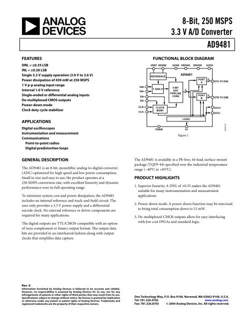
8-<strong>Bit</strong>, <strong>250</strong> <strong>MSPS</strong><br />
<strong>3.3</strong> V A/D <strong>Converter</strong><br />
<strong>AD9481</strong><br />
FUNCTIONAL BLOCK DIAGRAM<br />
VREF SENSE<br />
REFERENCE<br />
T AND H<br />
CLOCK<br />
MGMT<br />
AGND DRGND DRVDD AVDD<br />
8-BIT<br />
ADC<br />
PIPELINE<br />
CORE<br />
<strong>AD9481</strong><br />
8<br />
PORT<br />
A<br />
PORT<br />
B<br />
8<br />
8<br />
D7A TO D0A<br />
D7B TO D0B<br />
DCO+<br />
DCO–<br />
APPLICATIONS<br />
Digital oscilloscopes<br />
Instrumentation and measurement<br />
Communications<br />
Point-to-point radios<br />
Digital predistortion loops<br />
PDWN<br />
LOGIC<br />
S1<br />
Figure 1.<br />
05045-001<br />
GENERAL DESCRIPTION<br />
The <strong>AD9481</strong> is an 8-bit, monolithic analog-to-digital converter<br />
(ADC) optimized for high speed and low power consumption.<br />
Small in size and easy to use, the product operates at a<br />
<strong>250</strong> <strong>MSPS</strong> conversion rate, with excellent linearity and dynamic<br />
performance over its full operating range.<br />
To minimize system cost and power dissipation, the <strong>AD9481</strong><br />
includes an internal reference and track-and-hold circuit. The<br />
user only provides a <strong>3.3</strong> V power supply and a differential<br />
encode clock. No external reference or driver components are<br />
required for many applications.<br />
The digital outputs are TTL/CMOS-compatible with an option<br />
of twos complement or binary output format. The output data<br />
bits are provided in an interleaved fashion along with output<br />
clocks that simplifies data capture.<br />
The <strong>AD9481</strong> is available in a Pb-free, 44-lead, surface-mount<br />
package (TQFP-44) specified over the industrial temperature<br />
range (−40°C to +85°C).<br />
PRODUCT HIGHLIGHTS<br />
1. Superior linearity. A DNL of ±0.35 makes the <strong>AD9481</strong><br />
suitable for many instrumentation and measurement<br />
applications<br />
2. Power-down mode. A power-down function may be exercised<br />
to bring total consumption down to 15 mW.<br />
3. De-multiplexed CMOS outputs allow for easy interfacing<br />
with low cost FPGAs and standard logic.<br />
Rev. 0<br />
Information furnished by <strong>Analog</strong> <strong>Devices</strong> is believed to be accurate and reliable.<br />
However, no responsibility is assumed by <strong>Analog</strong> <strong>Devices</strong> for its use, nor for any<br />
infringements of patents or other rights of third parties that may result from its use.<br />
Specifications subject to change without notice. No license is granted by implication<br />
or otherwise under any patent or patent rights of <strong>Analog</strong> <strong>Devices</strong>. Trademarks and<br />
registered trademarks are the property of their respective owners.<br />
One Technology Way, P.O. Box 9106, Norwood, MA 02062-9106, U.S.A.<br />
Tel: 781.329.4700<br />
www.analog.com<br />
Fax: 781.326.8703 © 2004 <strong>Analog</strong> <strong>Devices</strong>, Inc. All rights reserved.
<strong>AD9481</strong><br />
TABLE OF CONTENTS<br />
DC Specifications ............................................................................. 3<br />
Digital Specifications........................................................................ 4<br />
AC Specifications.............................................................................. 5<br />
Switching Specifications .................................................................. 6<br />
Timing Diagram ........................................................................... 7<br />
Absolute Maximum Ratings............................................................ 8<br />
Explanation of Test Levels........................................................... 8<br />
ESD Caution.................................................................................. 8<br />
Pin Configuration and Function Descriptions............................. 9<br />
Terminology .................................................................................... 10<br />
Typical Performance Characteristics ........................................... 12<br />
Equivalent Circuits ......................................................................... 16<br />
Applications..................................................................................... 17<br />
<strong>Analog</strong> Inputs.............................................................................. 17<br />
Voltage Reference ....................................................................... 17<br />
Clocking the <strong>AD9481</strong>................................................................. 19<br />
DS Inputs ..................................................................................... 19<br />
Digital Outputs ........................................................................... 20<br />
Data Clock Out........................................................................... 20<br />
Power-Down Input..................................................................... 20<br />
<strong>AD9481</strong> Evaluation Board ............................................................ 21<br />
Power Connector........................................................................ 21<br />
<strong>Analog</strong> Inputs.............................................................................. 21<br />
Gain.............................................................................................. 21<br />
Optional Operational Amplifier............................................... 21<br />
Clock ............................................................................................ 21<br />
Optional Clock Buffer ............................................................... 21<br />
DS ................................................................................................. 21<br />
Optional XTAL ........................................................................... 22<br />
Voltage Reference ....................................................................... 22<br />
Data Outputs............................................................................... 22<br />
Evaluation Board Bill of Materials (BOM) ................................. 23<br />
PCB Schematics .............................................................................. 24<br />
PCB Layers ...................................................................................... 26<br />
Outline Dimensions ....................................................................... 28<br />
Ordering Guide .......................................................................... 28<br />
Interleaving Two <strong>AD9481</strong>s........................................................ 20<br />
REVISION HISTORY<br />
10/04—Revision 0: Initial Version<br />
Rev. 0 | Page 2 of 28
DC SPECIFICATIONS<br />
<strong>AD9481</strong><br />
AVDD = <strong>3.3</strong> V, DRVDD = <strong>3.3</strong> V; TMIN = −40°C, TMAX = +85°C, AIN = −1 dBFS, full scale = 1.0 V, internal reference, differential analog and<br />
clock inputs, unless otherwise noted.<br />
Table 1.<br />
<strong>AD9481</strong>-<strong>250</strong><br />
Parameter Temp Test Level Min Typ Max Unit<br />
RESOLUTION 8 <strong>Bit</strong>s<br />
ACCURACY<br />
No Missing Codes Full VI Guaranteed<br />
Offset Error 25°C I −40 40 mV<br />
Gain Error 1 25°C I −6.0 6.0 % FS<br />
Differential Nonlinearity (DNL) Full VI −0.85 ±0.35 0.85 LSB<br />
Integral Nonlinearity (INL) Full VI −0.9 ±0.26 0.9 LSB<br />
TEMPERATURE DRIFT<br />
Offset Error Full V 30 µV/°C<br />
Gain Error Full V 0.03 % FS/°C<br />
Reference Full V ±0.025 mV/°C<br />
REFERENCE<br />
Internal Reference Voltage Full VI 0.97 1.0 1.03 V<br />
Output Current 2 25°C IV 1.5 mA<br />
IVREF Input Current 3 25°C I 100 µA<br />
ISENSE Input Current 2 25°C I 10 µA<br />
ANALOG INPUTS (VIN+, VIN−)<br />
Differential Input Voltage Range 4 Full V 1 V p-p<br />
Common-Mode Voltage Full VI 1.6 1.9 2.1 V<br />
Input Resistance Full VI 8.4 10 11.2 kΩ<br />
Input Capacitance 25°C V 4 pF<br />
<strong>Analog</strong> Bandwidth, Full Power 25°C V 750 MHz<br />
POWER SUPPLY<br />
AVDD Full IV 3.0 <strong>3.3</strong> 3.6 V<br />
DRVDD Full IV 3.0 <strong>3.3</strong> 3.6 V<br />
Supply Currents<br />
IAVDD 5 Full VI 133 145 mA<br />
IDRVDD 5 Full VI 39 42.5 mA<br />
Power Dissipation 5 25°C V 439 mW<br />
Power-Down Dissipation 25°C V 15 37 mW<br />
Power Supply Rejection Ratio (PSRR) 25°C V −4.2 mV/V<br />
1<br />
Gain error and gain temperature coefficients are based on the ADC only (with a fixed 1 V external reference and 1 V p-p input range).<br />
2<br />
Internal reference mode; SENSE = AGND.<br />
3<br />
External reference mode; VREF driven by external 1.0 V reference; SENSE = AVDD.<br />
4<br />
In FS = 1 V, both analog inputs are 500 mV p-p and out of phase with each other.<br />
5 Supply current measured with rated encode and a 20 MHz analog input. Power dissipation measured with dc input, see the T erminology section for power vs. clock<br />
rate.<br />
Rev. 0 | Page 3 of 28
<strong>AD9481</strong><br />
DIGITAL SPECIFICATIONS<br />
AVDD = <strong>3.3</strong> V, DRVDD = <strong>3.3</strong> V; TMIN = −40°C, TMAX = +85°C, AIN = −1 dBFS, full scale = 1.0 V, internal reference, differential analog and<br />
clock inputs, unless otherwise noted.<br />
Table 2.<br />
<strong>AD9481</strong>-<strong>250</strong><br />
Parameter Temp Test Level Min Typ Max Unit<br />
CLOCK AND DS INPUTS (CLK+, CLK−, DS+, DS−)<br />
Differential Input Full IV 200 mV p-p<br />
Common-Mode Voltage 1 Full VI 1.38 1.5 1.68 V<br />
Input Resistance Full VI 4.2 5.5 6.0 kΩ<br />
Input Capacitance 25°C V 4 pF<br />
LOGIC INPUTS (PDWN, S1)<br />
Logic 1 Voltage Full IV 2.0 V<br />
Logic 0 Voltage Full IV 0.8 V<br />
Logic 1 Input Current Full VI ±160 µA<br />
Logic 0 input Current Full VI 10 µA<br />
Input Resistance 25°C V 30 kΩ<br />
Input Capacitance 25°C V 4 pF<br />
DIGITAL OUTPUTS<br />
Logic 1 Voltage 2 Full VI DRVDD − 0.05 mV<br />
Logic 0 Voltage Full VI 0.05 V<br />
Output Coding Full IV Twos complement or binary<br />
1<br />
The common mode for CLOCK inputs can be externally set, such that 0.9 V < CLK ± < 2.6 V.<br />
2<br />
Capacitive loading only.<br />
Rev. 0 | Page 4 of 28
AC SPECIFICATIONS<br />
<strong>AD9481</strong><br />
AVDD = <strong>3.3</strong> V, DRVDD = <strong>3.3</strong> V; TMIN = −40°C, TMAX = +85°C, AIN = −1 dBFS, full scale = 1.0 V, internal reference, differential analog and<br />
clock inputs, unless otherwise noted.<br />
Table 3.<br />
<strong>AD9481</strong>-<strong>250</strong><br />
Parameter Temp Test Level Min Typ Max Unit<br />
SIGNAL-TO-NOISE RATIO (SNR)<br />
fIN = 19.7 MHz 25°C V 46 dB<br />
fIN = 70.1 MHz 25°C I 44.5 45.7 dB<br />
SIGNAL-TO-NOISE AND DISTORTION (SINAD)<br />
fIN = 19.7 MHz 25°C V 45.9 dB<br />
fIN = 70.1 MHz 25°C I 44.4 45.7 dB<br />
EFFECTIVE NUMBER OF BITS (ENOB)<br />
fIN = 19.7 MHz 25°C V 7.5 <strong>Bit</strong>s<br />
fIN = 70.1 MHz 25°C I 7.2 7.5 <strong>Bit</strong>s<br />
WORST SECOND OR THIRD HARMONIC DISTORTION<br />
fIN = 19.7 MHz 25°C V −64.8 dBc<br />
fIN = 70.1 MHz 25°C I −64.8 −54 dBc<br />
WORST OTHER<br />
fIN = 19.7 MHz 25°C V −68 dBc<br />
fIN = 70.1 MHz 25°C I −65.8 −56 dBc<br />
SPURIOUS-FREE DYNAMIC RANGE (SFDR) 1<br />
fIN = 19.7 MHz 25°C V −64.8 dBc<br />
fIN = 70.1 MHz 25°C I −64.8 −54 dBc<br />
TWO-TONE INTERMODULATION DISTORTION (IMD)<br />
fIN1 = 69.3 MHz, fIN2 = 70.3 MHz 25°C V −64.9 dBc<br />
1<br />
DC and Nyquist bin energy ignored.<br />
Rev. 0 | Page 5 of 28
<strong>AD9481</strong><br />
SWITCHING SPECIFICATIONS<br />
AVDD = <strong>3.3</strong> V, DRVDD = <strong>3.3</strong> V; differential encode input, duty cycle stabilizer enabled, unless otherwise noted.<br />
Table 4.<br />
<strong>AD9481</strong>-<strong>250</strong><br />
Parameter Temp Test Level Min Typ Max Unit<br />
CLOCK<br />
Maximum Conversion Rate Full VI <strong>250</strong> <strong>MSPS</strong><br />
Minimum Conversion Rate Full IV 20 <strong>MSPS</strong><br />
Clock Pulse-Width High (tEH) Full IV 1.2 2 ns<br />
Clock Pulse-Width Low (tEL) Full IV 1.2 2 ns<br />
DS Input Setup Time (tSDS) Full IV 0.5 ns<br />
DS Input Hold Time (tHDS) Full IV 0.5 ns<br />
OUTPUT PARAMETERS 1<br />
Valid Time (tV) 2 Full VI 2.5 ns<br />
Propagation Delay (tPD) Full VI 4 5.4 ns<br />
Rise Time (tR) 10% to 90% Full V 670 ps<br />
Fall Time (tF) 10% to 90% Full V 360 ps<br />
DCO Propagation Delay (tCPD) 3 Full VI 2.5 3.9 5.3 ns<br />
Data-to-DCO Skew (tPD − tCPD) 4 Full VI −0.5 +0.5 ns<br />
A Port Data to DCO− Rising (tSKA) 5 Full IV 4 ns<br />
B Port Data to DCO+ Rising (tSKB) Full IV 4 ns<br />
Pipeline Latency (A, B) Full IV 8 Cycles<br />
APERTURE<br />
Aperture Delay (tA) 25°C V 1.5 ns<br />
Aperture Uncertainty (Jitter) 25°C V 0.25 ps rms<br />
OUT-OF-RANGE RECOVERY TIME 25°C V 1 Cycle<br />
1<br />
CLOAD equals 5 pF maximum for all output switching specifications.<br />
2<br />
Valid time is approximately equal to minimum tPD.<br />
3<br />
TCPD equals clock rising edge to DCO (+ or −) rising edge delay.<br />
4<br />
Data changing to (DCO+ or DCO−) rising edge delay.<br />
5<br />
TSKA, TSKB are both clock rate dependent delays equal to TCYCLE − (Data to DCO skew).<br />
Rev. 0 | Page 6 of 28
<strong>AD9481</strong><br />
TIMING DIAGRAM<br />
VIN<br />
N–1<br />
N<br />
t A<br />
N+8<br />
N+9<br />
N+10<br />
N+1<br />
N+7<br />
8 CYCLES<br />
CLK+<br />
t EH<br />
t EL<br />
1/f S<br />
CLK–<br />
DS+<br />
t HDS<br />
DS–<br />
t SDS<br />
INTERLEAVED DATA OUT<br />
t PD<br />
t V<br />
PORT A<br />
STATIC INVALID N<br />
D7A TO D0A<br />
PORT B<br />
D7B TO D0B<br />
DCO+<br />
DCO–<br />
STATIC INVALID INVALID N+1<br />
t SKA<br />
t<br />
t SKB<br />
CPD<br />
STATIC<br />
05045-002<br />
Figure 2. Timing Diagram<br />
Rev. 0 | Page 7 of 28
<strong>AD9481</strong><br />
ABSOLUTE MAXIMUM RATINGS<br />
Thermal impedance (θJA) = 46.4°C/W (4-layer PCB).<br />
EXPLANATION OF TEST LEVELS<br />
Table 5.<br />
Parameter<br />
Min.<br />
Rating<br />
Max.<br />
Rating<br />
ELECTRICAL<br />
AVDD (With respect to AGND) −0.5 V +4.0 V<br />
DRVDD<br />
−0.5 V +4.0 V<br />
(With respect to DRGND)<br />
AGND (With respect to DRGND) −0.5 V +0.5 V<br />
Digital I/0<br />
−0.5 V DRVDD + 0.5 V<br />
(With respect to DRGND)<br />
<strong>Analog</strong> Inputs<br />
−0.5 V AVDD + 0.5 V<br />
(With respect to AGND)<br />
ENVIRONMENTAL<br />
Operating Temperature −40°C +85°C<br />
Junction Temperature 150°C<br />
Storage Temperature 150°C<br />
Stresses above those listed under Absolute Maximum Ratings<br />
may cause permanent damage to the device. This is a stress<br />
rating only; functional operation of the device at these or any<br />
other conditions above those indicated in the operational<br />
section of this specification is not implied. Exposure to absolute<br />
maximum rating conditions for extended periods may affect<br />
device reliability.<br />
Table 6.<br />
Level Description<br />
I 100% production tested.<br />
II 100% production tested at 25°C and guaranteed by<br />
design and characterization at specified temperatures.<br />
III Sample tested only.<br />
IV Parameter is guaranteed by design and characterization<br />
testing.<br />
V Parameter is a typical value only.<br />
VI 100% production tested at 25°C and guaranteed by<br />
design and characterization for industrial temperature<br />
range.<br />
ESD CAUTION<br />
ESD (electrostatic discharge) sensitive device. Electrostatic charges as high as 4000 V readily accumulate<br />
on the human body and test equipment and can discharge without detection. Although this product features<br />
proprietary ESD protection circuitry, permanent damage may occur on devices subjected to high energy<br />
electrostatic discharges. Therefore, proper ESD precautions are recommended to avoid performance<br />
degradation or loss of functionality.<br />
Rev. 0 | Page 8 of 28
<strong>AD9481</strong><br />
PIN CONFIGURATION AND FUNCTION DESCRIPTIONS<br />
44<br />
CLK+<br />
CLK–<br />
1<br />
2<br />
PIN 1<br />
33<br />
32<br />
SENSE<br />
AGND<br />
AVDD<br />
3<br />
31<br />
AVDD<br />
AGND<br />
DRVDD<br />
DRGND<br />
4<br />
5<br />
6<br />
30<br />
29<br />
28<br />
AVDD<br />
PDWN<br />
S1<br />
D7A (MSB)<br />
7<br />
27<br />
DRGND<br />
D6A<br />
8<br />
26<br />
D7B (MSB)<br />
D5A<br />
9<br />
25<br />
D6B<br />
D4A<br />
10<br />
24<br />
D5B<br />
D3A<br />
11<br />
23<br />
D4B<br />
12<br />
13<br />
14<br />
15<br />
16<br />
17<br />
18<br />
19<br />
20<br />
21<br />
22<br />
D2A<br />
D1A<br />
D0A (LSB)<br />
DRGND<br />
DCO–<br />
DCO+<br />
DRVDD<br />
D0B (LSB)<br />
D1B<br />
D2B<br />
D3B<br />
DS+<br />
DS–<br />
S3<br />
AVDD<br />
AGND<br />
VIN+<br />
VIN–<br />
AGND<br />
AVDD<br />
AGND<br />
VREF<br />
43<br />
42<br />
41<br />
40<br />
39<br />
38<br />
37<br />
36<br />
35<br />
34<br />
<strong>AD9481</strong><br />
TOP VIEW<br />
(Not to Scale)<br />
05045-003<br />
Figure 3. Pin Configuration<br />
Table 7. Pin Function Descriptions<br />
Pin<br />
No. Name Description<br />
1 CLK+ Input Clock—True<br />
2 CLK− Input Clock—Complement<br />
3 AVDD <strong>3.3</strong> V <strong>Analog</strong> Supply<br />
4 AGND <strong>Analog</strong> Ground<br />
5 DRVDD <strong>3.3</strong> V Digital Output Supply<br />
6 DRGND Digital Ground<br />
7 D7A Data Output <strong>Bit</strong> 7—Channel A (MSB)<br />
8 D6A Data Output <strong>Bit</strong> 6—Channel A<br />
9 D5A Data Output <strong>Bit</strong> 5—Channel A<br />
10 D4A Data Output <strong>Bit</strong> 4—Channel A<br />
11 D3A Data Output <strong>Bit</strong> 3—Channel A<br />
12 D2A Data Output <strong>Bit</strong> 2—Channel A<br />
13 D1A Data Output <strong>Bit</strong> 1—Channel A<br />
14 D0A Data Output <strong>Bit</strong> 0—Channel A (LSB)<br />
15 DRGND Digital Ground<br />
16 DCO− Data Clock Output—Complement<br />
17 DCO+ Data Clock Output—True<br />
18 DRVDD <strong>3.3</strong> V Digital Output Supply<br />
19 D0B Data Output <strong>Bit</strong> 0—Channel B (LSB)<br />
20 D1B Data Output <strong>Bit</strong> 1—Channel B<br />
21 D2B Data Output <strong>Bit</strong> 2—Channel B<br />
22 D3B Data Output <strong>Bit</strong> 3—Channel B<br />
23 D4B Data Output <strong>Bit</strong> 4—Channel B<br />
24 D5B Data Output <strong>Bit</strong> 5—Channel B<br />
Pin<br />
No. Name Description<br />
25 D6B Data Output <strong>Bit</strong> 6—Channel B<br />
26 D7B Data Output <strong>Bit</strong> 7—Channel B (MSB)<br />
27 DRGND Digital Ground<br />
28 S1 Data Format Select and Duty Cycle Stabilizer<br />
Select<br />
29 PDWN Power-Down Selection<br />
30 AVDD <strong>3.3</strong> V <strong>Analog</strong> Supply<br />
31 AVDD <strong>3.3</strong> V <strong>Analog</strong> Supply<br />
32 AGND <strong>Analog</strong> Ground<br />
33 SENSE Reference Mode Selection<br />
34 VREF Voltage Reference Input/Output<br />
35 AGND <strong>Analog</strong> Ground<br />
36 AVDD <strong>3.3</strong> V <strong>Analog</strong> Supply<br />
37 AGND <strong>Analog</strong> Ground<br />
38 VIN− <strong>Analog</strong> Input—Complement<br />
39 VIN+ <strong>Analog</strong> Input—True<br />
40 AGND <strong>Analog</strong> Ground<br />
41 AVDD <strong>3.3</strong> V <strong>Analog</strong> Supply<br />
42 S3 DCO Enable Select (Tie to AVDD for DCO<br />
Active)<br />
43 DS− Data Sync Complement (If Unused, Tie to<br />
DRVDD)<br />
44 DS+ Data Sync True (If Unused, Tie to DGND)<br />
Rev. 0 | Page 9 of 28
<strong>AD9481</strong><br />
TERMINOLOGY<br />
<strong>Analog</strong> Bandwidth<br />
The analog input frequency at which the spectral power of the<br />
fundamental frequency (as determined by the FFT analysis) is<br />
reduced by 3 dB.<br />
Aperture Delay<br />
The delay between the 50% point of the rising edge of the<br />
encode command and the instant the analog input is sampled.<br />
Aperture Uncertainty (Jitter)<br />
The sample-to-sample variation in aperture delay.<br />
Clock Pulse-Width/Duty Cycle<br />
Pulse-width high is the minimum amount of time that the clock<br />
pulse should be left in a Logic 1 state to achieve rated<br />
performance; pulse-width low is the minimum time clock pulse<br />
should be left in a low state. See timing implications of changing<br />
tEH in the Clocking the <strong>AD9481</strong> section. At a given clock rate,<br />
these specifications define an acceptable clock duty cycle.<br />
Crosstalk<br />
Coupling onto one channel being driven by a low level<br />
(−40 dBFS) signal when the adjacent interfering channel is<br />
driven by a full-scale signal.<br />
Differential <strong>Analog</strong> Input Resistance, Differential <strong>Analog</strong><br />
Input Capacitance, and Differential <strong>Analog</strong> Input Impedance<br />
The real and complex impedances measured at each analog<br />
input port. The resistance is measured statically and the<br />
capacitance and differential input impedances are measured<br />
with a network analyzer.<br />
Differential <strong>Analog</strong> Input Voltage Range<br />
The peak-to-peak differential voltage that must be applied to<br />
the converter to generate a full-scale response. Peak differential<br />
voltage is computed by observing the voltage on a single pin<br />
and subtracting the voltage from the other pin, which is 180°<br />
out of phase. Peak-to-peak differential is computed by rotating<br />
the inputs phase 180° and taking the peak measurement again.<br />
The difference is then computed between both peak<br />
measurements.<br />
Differential Nonlinearity<br />
The deviation of any code width from an ideal 1 LSB step.<br />
Effective Number of <strong>Bit</strong>s (ENOB)<br />
ENOB is calculated from the measured SINAD based on the<br />
equation (assuming full-scale input)<br />
ENOB =<br />
SINAD MEASURED<br />
6.02<br />
− 1.76 dB<br />
Full-Scale Input Power<br />
Expressed in dBm. Computed using the following equation<br />
Power<br />
FULLSCALE<br />
=<br />
⎛ V<br />
⎜<br />
⎜<br />
log ⎜<br />
⎜<br />
⎝<br />
2<br />
FULLSCALE<br />
Z<br />
0.001<br />
10<br />
INPUT<br />
rms ⎞<br />
⎟<br />
⎟<br />
⎟<br />
⎟<br />
⎠<br />
Gain Error<br />
Gain error is the difference between the measured and ideal<br />
full-scale input voltage range of the ADC.<br />
Harmonic Distortion, Second<br />
The ratio of the rms signal amplitude to the rms value of the<br />
second harmonic component, reported in dBc.<br />
Harmonic Distortion, Third<br />
The ratio of the rms signal amplitude to the rms value of the<br />
third harmonic component, reported in dBc.<br />
Integral Nonlinearity<br />
The deviation of the transfer function from a reference line<br />
measured in fractions of 1 LSB using a best straight line<br />
determined by a least square curve fit.<br />
Minimum Conversion Rate<br />
The encode rate at which the SNR of the lowest analog signal<br />
frequency drops by no more than 3 dB below the guaranteed<br />
limit.<br />
Maximum Conversion Rate<br />
The encode rate at which parametric testing is performed.<br />
Output Propagation Delay<br />
The delay between a differential crossing of CLK+ and CLK−<br />
and the time when all output data bits are within valid logic<br />
levels.<br />
Noise (for Any Range within the ADC)<br />
This value includes both thermal and quantization noise.<br />
V<br />
where:<br />
noise<br />
=<br />
⎛ FS<br />
Z × 0 .001×<br />
10 ⎜<br />
⎝<br />
Z is the input impedance.<br />
dBm<br />
− SNRdBc<br />
− Signal<br />
10<br />
dBFS<br />
FS is the full scale of the device for the frequency in question.<br />
SNR is the value for the particular input level.<br />
Signal is the signal level within the ADC reported in dB below<br />
full scale.<br />
⎞<br />
⎟<br />
⎠<br />
Rev. 0 | Page 10 of 28
<strong>AD9481</strong><br />
Power Supply Rejection Ratio<br />
The ratio of a change in input offset voltage to a change in<br />
power supply voltage.<br />
Signal-to-Noise and Distortion (SINAD)<br />
The ratio of the rms signal amplitude (set 1 dB below full scale)<br />
to the rms value of the sum of all other spectral components,<br />
including harmonics, but excluding dc.<br />
Signal-to-Noise Ratio (without Harmonics)<br />
The ratio of the rms signal amplitude (set at 1 dB below full<br />
scale) to the rms value of the sum of all other spectral<br />
components, excluding the first five harmonics and dc.<br />
Spurious-Free Dynamic Range (SFDR)<br />
The ratio of the rms signal amplitude to the rms value of the<br />
peak spurious spectral component. The peak spurious<br />
component may or may not be a harmonic. It also may be<br />
reported in dBc (degrades as signal level is lowered) or dBFS<br />
(always related back to converter full scale).<br />
Two-Tone Intermodulation Distortion Rejection<br />
The ratio of the rms value of either input tone to the rms value<br />
of the worst third-order intermodulation product, in dBc.<br />
Two-Tone SFDR<br />
The ratio of the rms value of either input tone to the rms value<br />
of the peak spurious component. The peak spurious component<br />
may or may not be an IMD product. It also may be reported in<br />
dBc (degrades as signal level is lowered) or in dBFS (always<br />
relates back to converter full scale).<br />
Worst Other Spur<br />
The ratio of the rms signal amplitude to the rms value of the<br />
worst spurious component (excluding the second and third<br />
harmonic), reported in dBc.<br />
Transient Response Time<br />
The time it takes for the ADC to reacquire the analog input<br />
after a transient from 10% above negative full scale to 10%<br />
below positive full scale.<br />
Out-of-Range Recovery Time<br />
This is the time it takes for the ADC to reacquire the analog<br />
input after a transient from 10% above positive full scale to 10%<br />
above negative full scale, or from 10% below negative full scale<br />
to 10% below positive full scale.<br />
Rev. 0 | Page 11 of 28
<strong>AD9481</strong><br />
TYPICAL PERFORMANCE CHARACTERISTICS<br />
AVDD, DRVDD = <strong>3.3</strong> V, T = 25°C, AIN differential drive, FS = 1, internal reference mode, unless otherwise noted.<br />
0<br />
–10<br />
–20<br />
SNR = 45.8dB<br />
H2 = –65.2dBc<br />
H3 = –63.2dBc<br />
SFDR = 63.2dBc<br />
0<br />
–10<br />
–20<br />
SNR = 45.6dB<br />
H2 = –72.9dBc<br />
H3 = –65.2dBc<br />
SFDR = 59.6dBc<br />
–30<br />
–30<br />
–40<br />
–40<br />
(dB)<br />
–50<br />
(dB)<br />
–50<br />
–60<br />
–60<br />
–70<br />
–70<br />
–80<br />
–90<br />
0 20 40 60 80 100 120<br />
(MHz)<br />
05045-004<br />
–80<br />
–90<br />
0 20 40 60 80 100 120<br />
(MHz)<br />
05045-007<br />
Figure 4. FFT: fS = <strong>250</strong> <strong>MSPS</strong>, AIN = 10.3 MHz @ −1 dBFS<br />
Figure 7. FFT: fS = <strong>250</strong> <strong>MSPS</strong>, AIN = 170 MHz @ −1 dBFS<br />
(dB)<br />
(dB)<br />
0<br />
–10<br />
–20<br />
–30<br />
–40<br />
–50<br />
–60<br />
–70<br />
–80<br />
SNR = 45.8dB<br />
H2 = –68.5dBc<br />
H3 = –63.5dBc<br />
SFDR = 63.8dBc<br />
–90<br />
0 20 40 60 80 100 120<br />
(MHz)<br />
0<br />
–10<br />
–20<br />
–30<br />
–40<br />
–50<br />
–60<br />
–70<br />
–80<br />
Figure 5. FFT: fS = <strong>250</strong> <strong>MSPS</strong>, AIN = 70 MHz @ −1 dBFS<br />
SNR = 45.9dB<br />
H2 = –66.6dBc<br />
H3 = –70.1dBc<br />
SFDR = 65.9dBc<br />
–90<br />
0 20 40 60 80 100 120<br />
(MHz)<br />
Figure 6. FFT: fS = <strong>250</strong> <strong>MSPS</strong>, AIN = 70 MHz @ −1 dBFS, Single-Ended Input<br />
05045-005<br />
05045-006<br />
(dB)<br />
(dB)<br />
90<br />
85<br />
80<br />
75<br />
70<br />
65<br />
60<br />
55<br />
50<br />
45<br />
H3<br />
SFDR<br />
SNR<br />
SINAD<br />
40<br />
0 50 100 150 200 <strong>250</strong> 300 350 400<br />
A IN (MHz)<br />
90<br />
85<br />
80<br />
75<br />
70<br />
65<br />
60<br />
55<br />
50<br />
45<br />
H2<br />
Figure 8. <strong>Analog</strong> Input Frequency Sweep,<br />
AIN = −1 dBFS, FS = 1 V, fS = <strong>250</strong> <strong>MSPS</strong><br />
SFDR<br />
H3<br />
SNR<br />
SINAD<br />
40<br />
0 50 100 150 200 <strong>250</strong> 300 350 400<br />
A IN (MHz)<br />
Figure 9. <strong>Analog</strong> Input Frequency Sweep,<br />
AIN =−1 dBFS, FS = 0.75 V, fS = <strong>250</strong> <strong>MSPS</strong>, External VREF Mode<br />
H2<br />
05045-008<br />
05045-009<br />
Rev. 0 | Page 12 of 28
<strong>AD9481</strong><br />
75<br />
140<br />
70<br />
SFDR<br />
120<br />
I AVDD<br />
(dB)<br />
65<br />
60<br />
55<br />
CURRENT (mA)<br />
100<br />
80<br />
60<br />
50<br />
45<br />
SNR<br />
SINAD<br />
40<br />
0 50 100 150 200 <strong>250</strong> 300<br />
SAMPLE CLOCK (MHz)<br />
Figure 10. SNR, SINAD, SFDR vs. Sample Clock Frequency,<br />
AIN = 70 MHz @ −1 dB<br />
05045-010<br />
40<br />
20<br />
I DRVDD<br />
0<br />
0 50 100 150 200 <strong>250</strong> 300<br />
SAMPLE CLOCK (<strong>MSPS</strong>)<br />
Figure 13. IAVDD and IDRVDD vs. Clock Rate, CLOAD = 5 pF<br />
AIN = 70 MHz @ −1 dBFS<br />
05045-013<br />
80<br />
50<br />
70<br />
60<br />
SFDR (dBFS)<br />
49<br />
48<br />
47<br />
DCS ON<br />
50<br />
46<br />
(dB)<br />
40<br />
30<br />
20<br />
10<br />
SFDR (dBc)<br />
60dB<br />
REFERENCE LINE<br />
0<br />
–70 –60 –50 –40 –30 –20 –10 0<br />
ANALOG INPUT DRIVE LEVEL (dBFS)<br />
05045-011<br />
(dB)<br />
45<br />
44<br />
43<br />
42<br />
41<br />
DCS OFF<br />
40<br />
20 30 40 50 60 70 80<br />
CLOCK POSITIVE DUTY CYCLE (%)<br />
05045-014<br />
Figure 11. SFDR vs. AIN Input Level; AIN = 70 MHz @ <strong>250</strong> <strong>MSPS</strong><br />
Figure 14. SNR, SINAD vs. Clock Pulse-Width High,<br />
AIN = 70 MHz @ −1 dBFS, <strong>250</strong> <strong>MSPS</strong>, DCS On/Off<br />
0<br />
–10<br />
F1, F2 = –7dBFS<br />
2F2–F1 = –65.9dBc<br />
2F1–F2 = –64.9dBc<br />
50.0<br />
75<br />
–20<br />
47.5<br />
SNR<br />
70<br />
(dB)<br />
–30<br />
–40<br />
–50<br />
–60<br />
SNR, SINAD (dB)<br />
45.0<br />
SINAD<br />
SFDR<br />
65<br />
SFDR (dBc)<br />
–70<br />
42.5<br />
60<br />
–80<br />
–90<br />
0 20 40 60 80 100 120<br />
(MHz)<br />
05045-012<br />
40.0<br />
0.5 0.7 0.9 1.1 1.3 1.5 1.7 1.9<br />
EXTERNAL VREF VOLTAGE (V)<br />
55<br />
05045-015<br />
Figure 12. Two-Tone Intermodulation Distortion<br />
(69.3 MHz and 70.3 MHz; fS = <strong>250</strong> <strong>MSPS</strong>)<br />
Figure 15. SNR, SINAD, and SFDR vs. VREF in External Reference Mode, AIN =<br />
70 MHz @ −1 dBFS, <strong>250</strong> <strong>MSPS</strong><br />
Rev. 0 | Page 13 of 28
<strong>AD9481</strong><br />
2.0<br />
70<br />
1.5<br />
1.0<br />
FS = 1V<br />
EXTERNAL REFERENCE<br />
65<br />
SFDR<br />
GAIN ERROR (%)<br />
0.5<br />
0<br />
–0.5<br />
(dB)<br />
60<br />
55<br />
–1.0<br />
–1.5<br />
FS = 1V<br />
INTERNAL REFERENCE<br />
–2.0<br />
–40 –20 0 20 40 60 80<br />
TEMPERATURE (°C)<br />
05045-016<br />
50<br />
SINAD<br />
45<br />
3.0 3.1 3.2 <strong>3.3</strong> 3.4<br />
AVDD (V)<br />
SNR<br />
3.5 3.6<br />
05045-019<br />
Figure 16. Full-Scale Gain Error vs. Temperature,<br />
AIN = 70.3 MHz @ −0.5 dBFS, <strong>250</strong> <strong>MSPS</strong><br />
Figure 19. SNR, SINAD, and SFDR vs. Supply Voltage,<br />
AIN = 70.3 MHz @ −1 dBFS, <strong>250</strong> <strong>MSPS</strong><br />
70<br />
65<br />
60<br />
SFDR<br />
0.5<br />
0.4<br />
0.3<br />
0.2<br />
0.1<br />
(dB)<br />
55<br />
LSB<br />
0<br />
50<br />
45<br />
SINAD<br />
40<br />
–40 –20 0 20 40 60 80<br />
TEMPERATURE (°C)<br />
05045-017<br />
–0.1<br />
–0.2<br />
–0.3<br />
–0.4<br />
–0.5<br />
0 50 100 150 200 <strong>250</strong><br />
CODE<br />
05045-020<br />
Figure 17. SINAD, SFDR vs. Temperature,<br />
AIN = 70 MHz @ −1 dBFS, <strong>250</strong> <strong>MSPS</strong><br />
Figure 20. Typical DNL Plot,<br />
AIN = 10.3 MHz @ −0.5 dBFS, <strong>250</strong> <strong>MSPS</strong><br />
0.10<br />
0.50<br />
0.05<br />
0.25<br />
CHANGE IN VREF (%)<br />
0<br />
–0.05<br />
–0.10<br />
LSB<br />
0<br />
–0.25<br />
–0.15<br />
2.7 2.8 2.9 3.0 3.1 3.2 <strong>3.3</strong> 3.4 3.5 3.6<br />
AVDD (V)<br />
Figure 18. VREF Sensitivity to AVDD<br />
05045-018<br />
–0.50<br />
0 50 100 150 200 <strong>250</strong><br />
CODE<br />
Figure 21. Typical INL Plot,<br />
AIN = 10.3 MHz @ −0.5 dBFS, <strong>250</strong> <strong>MSPS</strong><br />
05045-021<br />
Rev. 0 | Page 14 of 28
<strong>AD9481</strong><br />
0.2<br />
T PD _F<br />
DELAY CHANGE (ps)<br />
0.1<br />
0<br />
–0.1<br />
–0.2<br />
T CPD _F<br />
T CPD _R<br />
–0.3<br />
T PD _R<br />
–0.4<br />
–40 –20 0 20 40 60 80<br />
TEMPERATURE (°C)<br />
05045-048<br />
Figure 22. Propagation Delay Sensitivity vs. Temperature<br />
Rev. 0 | Page 15 of 28
<strong>AD9481</strong><br />
EQUIVALENT CIRCUITS<br />
AVDD<br />
AVDD<br />
16.7kΩ<br />
16.7kΩ<br />
VIN+<br />
150Ω<br />
150Ω<br />
VIN–<br />
PDWN<br />
25kΩ<br />
1.2pF<br />
25kΩ<br />
1.2pF<br />
30kΩ<br />
05045-023<br />
Figure 23. <strong>Analog</strong> Inputs<br />
AVDD<br />
12kΩ<br />
12kΩ<br />
CLK+<br />
150Ω<br />
10kΩ<br />
150Ω<br />
10kΩ<br />
CLK–<br />
05045-024<br />
Figure 24. Clock Inputs<br />
VDD<br />
30kΩ<br />
S1<br />
05045-025<br />
05045-026<br />
Figure 26. Power-Down Input<br />
DRVDD<br />
05045-027<br />
Figure 27. Data, DCO Outputs<br />
Figure 25. S1 Input<br />
Rev. 0 | Page 16 of 28
<strong>AD9481</strong><br />
APPLICATIONS<br />
The <strong>AD9481</strong> uses a 1.5 bit per stage architecture. The analog<br />
inputs drive an integrated high bandwidth track-and-hold<br />
circuit that samples the signal prior to quantization by the 8-bit<br />
core. For ease of use, the part includes an on-board reference<br />
and input logic that accepts TTL, CMOS, or LVPECL levels. The<br />
digital output logic levels are CMOS-compatible.<br />
ANALOG INPUTS<br />
The analog input to the <strong>AD9481</strong> is a differential buffer. For best<br />
dynamic performance, impedances at VIN+ and VIN− should<br />
match. Optimal performance is obtained when the analog<br />
inputs are driven differentially. SNR and SINAD performance<br />
can degrade if the analog input is driven with a single-ended<br />
signal. The analog inputs self-bias to approximately 1.9 V; this<br />
common-mode voltage can be externally overdriven by<br />
approximately ±300 mV if required.<br />
A wideband transformer, such as the Mini-Circuits ADT1-1WT,<br />
can provide the differential analog inputs for applications that<br />
require a single-ended-to-differential conversion. Note that the<br />
filter and center-tap capacitor on the secondary side is optional<br />
and dependent on application requirements. An RC filter at the<br />
secondary side helps reduce any wideband noise getting aliased<br />
by the ADC.<br />
49.9Ω<br />
0.1µF<br />
(R, C OPTIONAL)<br />
33Ω<br />
10pF<br />
33Ω<br />
VIN+<br />
AVDD<br />
<strong>AD9481</strong><br />
VIN–<br />
AGND<br />
Figure 28. Driving the ADC with an RF Transformer<br />
For dc-coupled applications, the AD8138/AD8139 or AD8351<br />
can serve as a convenient ADC driver, depending on<br />
requirements. Figure 29 shows an example with the AD8138.<br />
The <strong>AD9481</strong> PCB has an optional AD8351 on board, as shown<br />
in Figure 39 and Figure 40. The AD8351 typically yields better<br />
performance for frequencies greater than 30 MHz to 40 MHz.<br />
The <strong>AD9481</strong>’s linearity and SFDR start to degrade at higher<br />
analog frequencies (see the Typical Performance Characteristics<br />
section). For higher frequency applications, the AD9480 with<br />
LVDS outputs and superior AC performance should be<br />
considered.<br />
05045-029<br />
0.1µF<br />
1.3kΩ<br />
49.9Ω<br />
2kΩ<br />
499Ω<br />
523Ω<br />
499Ω<br />
AD8138<br />
499Ω<br />
33Ω<br />
20pF<br />
33Ω<br />
VIN+<br />
AVDD<br />
<strong>AD9481</strong><br />
VIN–<br />
Figure 29. Driving the ADC with the AD8138<br />
AGND<br />
The <strong>AD9481</strong> can be easily configured for different full-scale<br />
ranges. See the Voltage Reference section for more information.<br />
Optimal performance is achieved with a 1 V p-p analog input.<br />
SENSE = GND<br />
VIN+<br />
500mV 2.0V<br />
2.0V<br />
VIN–<br />
DIGITALOUT = ALL 1s<br />
VOLTAGE REFERENCE<br />
Figure 30. <strong>Analog</strong> Input Full Scale<br />
DIGITALOUT = ALL 0s<br />
A stable and accurate 1.0 V reference is built into the <strong>AD9481</strong>.<br />
Users can choose this internal reference or provide an external<br />
reference for greater accuracy and flexibility. Figure 32 shows<br />
the typical reference variation with temperature. Table 8<br />
summarizes the available reference configurations.<br />
VIN+<br />
VIN–<br />
VREF<br />
10µF + 0.1µF<br />
SENSE<br />
7kΩ<br />
SELECT<br />
LOGIC<br />
ADC<br />
CORE<br />
05045-030<br />
05045-031<br />
7kΩ<br />
0.5V<br />
05045-032<br />
Figure 31. Internal Reference Equivalent Circuit<br />
Rev. 0 | Page 17 of 28
<strong>AD9481</strong><br />
Fixed Reference<br />
The internal reference can be configured for a differential span<br />
of 1 V p-p (see Figure 34). It is recommended to place a 0.1 µF<br />
capacitor as close as possible to the VREF pin; a 10 µF capacitor<br />
is also required (see the PCB layout for guidance). If the internal<br />
reference of the <strong>AD9481</strong> is used to drive multiple converters to<br />
improve gain matching, the loading of the reference by the<br />
other converters must be considered. Figure 34 depicts how the<br />
internal reference voltage is affected by loading.<br />
1.0085<br />
0<br />
VREF<br />
10µF 0.1µF<br />
SENSE<br />
Figure 33. Internal Fixed Reference (1 V p-p)<br />
05045-034<br />
VREF (V)<br />
1.0080<br />
1.0075<br />
1.0070<br />
1.0065<br />
1.0060<br />
1.0055<br />
1.0050<br />
% CHANGE IN VREF VOLTAGE<br />
–0.1<br />
–0.2<br />
–0.3<br />
–0.4<br />
1.0045<br />
1.0040<br />
1.0035<br />
–40 –20 0 20 40 60 80<br />
TEMPERATURE (°C)<br />
Figure 32. Typical Reference Variation with Temperature<br />
05045-033<br />
–0.5<br />
0 0.5 1.0 1.5 2.0 2.5 3.0<br />
IREF (mA)<br />
Figure 34. Internal VREF vs. Load Current<br />
05045-035<br />
Table 8. Reference Configurations<br />
SENSE Voltage Resulting VREF Reference Differential Span<br />
AVDD N/A (external reference input) External 1 × external reference voltage<br />
0.5 V (Self-Biased) 0.5 × (1 + R1/R2) V Programmable 1 × VREF (0.75 V p-p to 1.5 V p-p)<br />
AGND to 0.2 V 1.0 V Internal fixed 1 V p-p<br />
Rev. 0 | Page 18 of 28
<strong>AD9481</strong><br />
External Reference<br />
An external reference can be used for greater accuracy and<br />
temperature stability when required. The gain of the <strong>AD9481</strong><br />
can also be varied using this configuration. A voltage output<br />
DAC can be used to set VREF, providing for a means to digitally<br />
adjust the full-scale voltage. VREF can be externally set to<br />
voltages from 0.75 V to 1.5 V; optimum performance is typically<br />
obtained at VREF = 1 V. (See the Typical Performance<br />
Characteristics section.)<br />
MAY REQUIRE<br />
RC FILTER<br />
EXTERNAL<br />
REFERENCE OR<br />
DAC INPUT<br />
AVDD<br />
VREF<br />
SENSE<br />
Figure 35. External Reference<br />
Programmable Reference<br />
The programmable reference can be used to set a differential<br />
input span anywhere between 0.75 V p-p and 1.5 V p-p by using<br />
an external resistor divider. The SENSE pin self-biases to 0.5 V,<br />
and the resulting VREF is equal to 0.5 × (1 + R1/R2). It is<br />
recommended to keep the sum of R1 + R2 ≥ 10 kΩ to limit<br />
VREF loading (for VREF = 1.5 V, set R1 equal to 7 kΩ and R2<br />
equal to 3.5 kΩ).<br />
10µF<br />
0.1µF<br />
CLOCKING THE <strong>AD9481</strong><br />
R1<br />
R2<br />
VREF<br />
SENSE<br />
Figure 36. Programmable Reference<br />
Any high speed ADC is extremely sensitive to the quality of the<br />
sampling clock provided by the user. A track-and-hold circuit is<br />
essentially a mixer, and any noise, distortion, or timing jitter on<br />
the clock is combined with the desired signal at the A/D output.<br />
Considerable care has been taken in the design of the CLOCK<br />
input of the <strong>AD9481</strong>, and the user is advised to give<br />
commensurate thought to the clock source.<br />
The <strong>AD9481</strong> has an internal clock duty cycle stabilization<br />
circuit that locks to the rising edge of CLOCK and optimizes<br />
timing internally for sample rates between 100 <strong>MSPS</strong> and<br />
<strong>250</strong> <strong>MSPS</strong>. This allows for a wide range of input duty cycles at<br />
the input without degrading performance. Jitter on the rising<br />
edge of the input is still of paramount concern and is not<br />
reduced by the internal stabilization circuit. The duty cycle<br />
control loop does not function for clock rates less than 70 MHz<br />
nominally. The loop has a time constant associated with it that<br />
needs to be considered in applications where the clock rate can<br />
05045-037<br />
05045--036<br />
change dynamically, requiring a wait time of 5 µs after a<br />
dynamic clock frequency increase before valid data is available.<br />
The clock duty cycle stabilizer can be disabled at Pin 28 (S1).<br />
The clock inputs are internally biased to 1.5 V (nominal) and<br />
support either differential or single-ended signals. For best<br />
dynamic performance, a differential signal is recommended. An<br />
MC100LVEL16 performs well in the circuit to drive the clock<br />
inputs (ac coupling is optional). If the clock buffer is greater<br />
than two inches from the ADC, a standard LVPECL<br />
termination may be required instead of the simple pull-down<br />
termination shown in Figure 37.<br />
DS INPUTS<br />
PECL<br />
GATE<br />
510kΩ<br />
0.1µF<br />
0.1µF<br />
510kΩ<br />
Figure 37. Clocking the <strong>AD9481</strong><br />
<strong>AD9481</strong><br />
CLK+<br />
CLK–<br />
The data sync inputs (DS+, DS−) can be used in applications<br />
which require that a given sample appear at a specific output<br />
port (A or B) relative to a given external timing signal.<br />
The DS inputs can also be used to synchronize two or more<br />
ADCs in a system to maintain phasing between Ports A and B on<br />
separate ADCs (in effect, synchronizing multiple DCO outputs).<br />
The DS inputs are internally biased to 1.5 V (nominal) and<br />
support either differential or single-ended signals. When DS+ is<br />
held high (DS− low), the ADC data outputs and DCO outputs<br />
do not switch and are held static. Synchronization is<br />
accomplished by the assertion (falling edge) of DS+ within the<br />
timing constraints tSDS and tHDS, relative to a clock rising edge.<br />
(On initial synchronization, tHDS is not relevant.) If DS+ falls<br />
within the required setup time (tSDS) before a given clock rising<br />
edge N, the analog value at that point in time is digitized and<br />
available at Port A, eight cycles later in interleaved mode. The<br />
next sample, N + 1, is sampled by the next rising clock edge and<br />
available at Port B, eight cycles after that clock edge.<br />
Driving each ADC’s DS inputs by the same sync signal<br />
accomplishes synchronization between multiple ADCs. In<br />
applications which require synchronization, one-shot<br />
synchronization is recommended. An easy way to accomplish<br />
synchronization is by a one-time sync at power-on reset.<br />
05045-028<br />
Rev. 0 | Page 19 of 28
<strong>AD9481</strong><br />
Table 9. S1 Voltage Levels<br />
S1 Voltage<br />
Data Format<br />
Duty Cycle<br />
Stabilizer<br />
(0.9 × AVDD) → AVDD Offset binary Disabled<br />
(2/3 × AVDD) ± (0.1 × AVDD) Offset binary Enabled<br />
(1/3 × AVDD) ± (0.1 × AVDD) Twos complement Enabled<br />
AGND → (0.1 × AVDD) Twos complement Disabled<br />
DIGITAL OUTPUTS<br />
The CMOS digital outputs are TTL-/CMOS-compatible for<br />
lower power consumption. The outputs are biased from a<br />
separate supply (DRVDD), allowing easy interface to external<br />
logic. The outputs are CMOS devices that swing from ground to<br />
DRVDD (with no dc load). It is recommended to minimize the<br />
capacitive load the ADC drives by keeping the output traces<br />
short (< 2 inch, for a total CLOAD < 5 pF). When operating in<br />
CMOS mode, it is also recommended to place low value series<br />
damping resistors on the data lines close to the ADC to reduce<br />
switching transient effects on performance.<br />
Table 10. Output Coding (FS = 1 V)<br />
Code (VIN+) − (VIN−) Offset Binary Twos Complement<br />
255 > +0.512 V 1111 1111 0111 1111<br />
255 +0.512 V 1111 1111 0111 1111<br />
254 +0.508 V 1111 1110 0111 1110<br />
• • • •<br />
• • • •<br />
129 +0.004 V 1000 0001 0000 0001<br />
128 +0.0 V 1000 0000 0000 0000<br />
127 −0.004 V 0111 1111 1111 1111<br />
• • • •<br />
• • • •<br />
2 −0.504 V 0000 0010 1000 0010<br />
1 −0.508 V 0000 0001 1000 0001<br />
0 −0.512 V 0000 0000 1000 0000<br />
0 < −0.512 V 0000 0000 1000 0000<br />
INTERLEAVING TWO <strong>AD9481</strong>s<br />
Instrumentation applications may prefer to interleave (or pingpong)<br />
two <strong>AD9481</strong>s to achieve twice the sample rate, or<br />
500 <strong>MSPS</strong>. In these applications, it is important to match the<br />
gain and offset of the two ADCs. Varying the reference voltage<br />
allows the gain of the ADCs to be adjusted; external dc offset<br />
compensation can be used to reduce offset mismatch between<br />
two ADCs. The sampling phase offset between the two ADCs<br />
is extremely important as well and requires very low skew<br />
between clock signals driving the ADCs (< 2 ps clock skew<br />
for a 100 MHz analog input frequency).<br />
DATA CLOCK OUT<br />
A data clock is available at DCO+ and DCO−. These clocks can<br />
facilitate latching off-chip, providing a low skew clocking<br />
solution. The on-chip delay of the DCO clocks tracks with the<br />
on-chip delay of the data bits, (under similar loading) such that<br />
the variation between tPD and tCPD is minimized. It is<br />
recommended to keep the trace lengths on the data and DCO<br />
pins matched and 2 inches maximum. A series damping resistor<br />
at the clock outputs is also recommended. The DCO outputs<br />
can be disabled and placed in a high impedance state by tying<br />
S3 to ground (tie to AVDD for DCO active). Switching both<br />
into and out of high impedance is accomplished in 4 ns from S3<br />
switching.<br />
POWER-DOWN INPUT<br />
The ADC can be placed into a low power state by setting the<br />
PDWN pin to AVDD. Time to go into (or come out of) power<br />
down equals 30 ns typically from PDWN switching.<br />
Rev. 0 | Page 20 of 28
<strong>AD9481</strong><br />
<strong>AD9481</strong> EVALUATION BOARD<br />
The <strong>AD9481</strong> evaluation board offers an easy way to test the<br />
device. It requires a clock source, an analog input signal, and a<br />
<strong>3.3</strong> V power supply. The clock source is buffered on the board to<br />
provide the clocks for the ADC and a data-ready signal. The<br />
digital outputs and output clocks are available at an 80-pin<br />
output connector, P3, P23. (Note that P3, P23 are represented<br />
schematically as two 40-pin connectors, and this connector is<br />
implemented as one 80-pin connector on the PCB.) The board<br />
has several different modes of operation and is shipped in the<br />
following configuration:<br />
• Offset binary<br />
• Internal voltage reference<br />
POWER CONNECTOR<br />
Power is supplied to the board via two detachable 4-pin power<br />
strips.<br />
Table 11. Power Connector<br />
Terminal<br />
Comments<br />
VDL (<strong>3.3</strong> V)<br />
AVDD 1 <strong>3.3</strong> V<br />
DRVDD 1 <strong>3.3</strong> V<br />
VCTRL 1 <strong>3.3</strong> V<br />
Op amp, ext. ref<br />
Output supply for external latches and data<br />
ready clock buffer ~ 30 mA<br />
<strong>Analog</strong> supply for ADC ~ 140 mA<br />
Output supply for ADC ~ 30 mA<br />
Supply for support clock circuitry ~ 60 mA<br />
Optional supply for op amp and ADR510<br />
reference<br />
1<br />
AVDD, DRVDD, VDL, and VCTRL are the minimum required power<br />
connections.<br />
ANALOG INPUTS<br />
The evaluation board accepts a 700 mV p-p analog input signal<br />
centered at ground at SMB Connector J3. This signal is<br />
terminated to ground through 50 Ω by R22. The input can be<br />
alternatively terminated at the T1 transformer secondary by<br />
R21 and R28. T1 is a wideband RF transformer that provides<br />
the single-ended-to-differential conversion, allowing the ADC<br />
to be driven differentially, minimizing even-order harmonics.<br />
An optional transformer, T4, can be placed if desired (remove<br />
T1, as shown in Figure 39 and Figure 40).<br />
The analog signal can be low-pass filtered by R21, C8 and R28,<br />
C9 at the ADC input.<br />
GAIN<br />
Full scale is set by the sense jumper. This jumper applies a bias<br />
to the SENSE pin to vary the full-scale range; the default<br />
position is SENSE = ground, setting the full scale to 1 V p-p.<br />
OPTIONAL OPERATIONAL AMPLIFIER<br />
The PCB has been designed to accommodate an optional<br />
AD8351 op amp that can serve as a convenient solution for dccoupled<br />
applications. To use the AD8351 op amp, remove R29,<br />
R31, and C3. Populate R12, R17, and R36 with 25 Ω resistors,<br />
and populate C1, C21, C23, C31, C39, and C30 with 0.1 µF<br />
capacitors. Populate R54, R10, and R11 with 10 Ω resistors, and<br />
R34 and R32 with 1 kΩ resistors. Populate R15 with a 1.2 kΩ<br />
resistor and R14 with a 100 Ω resistor. Populate R37 with a<br />
10 kΩ resistor.<br />
CLOCK<br />
The clock input is terminated to ground through 50 Ω at SMA<br />
Connector J1. The input is ac-coupled to a high speed<br />
differential receiver (LVEL16) that provides the required low<br />
jitter, fast edge rates needed for best performance. J1 input<br />
should be > 0.5 V p-p. Power to the LVEL16 is set to VCTRL<br />
(default) or AVDD by jumper placement at the device.<br />
OPTIONAL CLOCK BUFFER<br />
The PCB has been designed to accommodate the SNLVDS1 line<br />
driver. The SNLVDS1 is used as a high speed LVDS-level<br />
optional encode clock. To use this clock, please remove C2, C5,<br />
and C6. Place 0.1 µF capacitors on C34, C35, and C26. Place a<br />
10 Ω resistor on R48, and place a 100 Ω resistor on R6. Place a<br />
0 Ω resistor on both R49 and R53. For best results using the line<br />
driver, J1 input should be > 2.5 V p-p.<br />
DS<br />
The DS inputs are available on the PCB at J2 and J4. If driving<br />
DS+ externally, place a 0 Ω resistor at C48 and remove R53.<br />
Rev. 0 | Page 21 of 28
<strong>AD9481</strong><br />
OPTIONAL XTAL<br />
The PCB has been designed to accommodate an optional<br />
crystal oscillator that can serve as a convenient clock source.<br />
The footprint can accept both through-hole and surface-mount<br />
devices, including Vectron XO-400 and Vectron VCC6 family<br />
oscillators.<br />
VCC<br />
OUT–<br />
VCC<br />
Figure 38. XTAL Footprint<br />
OUT+<br />
GND<br />
05045-038<br />
To use either crystal, populate C38 and C40 with 0.1 µF capacitors.<br />
Populate R48 and R49 with 0 Ω resistors. Place R50, R51,<br />
R59, and R60 with 1 kΩ resistors. Remove C6 and C5. If the<br />
Vectron VCC6 family crystal is being used, populate R57 with a<br />
10 Ω resistor. If using the XO-400 crystal, place jumper E21 or<br />
E22 to E23.<br />
VOLTAGE REFERENCE<br />
The <strong>AD9481</strong> has an internal 1 V reference mode. The ADC uses<br />
the internal 1 V reference as the default when sense is set to<br />
ground. An optional on-board external 1.0 V reference<br />
(ADR510) can be used by setting the sense jumper to AVDD, by<br />
placing a jumper on E5 to E3, and by placing a 0 Ω resistor on<br />
R55. When using an external programmable reference, (R20,<br />
R30) remove the sense jumper.<br />
DATA OUTPUTS<br />
The ADC outputs are buffered on the PCB by LVT574 latches<br />
on the data outputs. The latch outputs have series terminating<br />
resistors at the output pins to minimize reflections.<br />
Rev. 0 | Page 22 of 28
EVALUATION BOARD BILL OF MATERIALS (BOM)<br />
Table 12.<br />
No. Quantity Reference Designator Device Package Value<br />
<strong>AD9481</strong><br />
1 24 C1 to C6, C10 to C12, C14 to C15,<br />
Capacitors 0402 0.1 µF<br />
C17 to C19, C22 to C29, C31, C48 to C49<br />
2 1 C13 Capacitor Tantalum (3528) 10 µF<br />
3 5 C32 to C36 Capacitors Tantalum (6032) 10 µF<br />
4 4 J1 to J4 SMA SMA Degrees<br />
5 3 P1, P12 to P13 4-pin power connectors Post Z5.531.3425.0<br />
6 3 P1, P12 to P13 4-pin power connectors Detachable connector 25.602.5453.0<br />
7 2 P3, P23 80-pin connectors Connector TSW-140-08-L-D-RA<br />
8 7 R1, R5, R19, R22, R27, R35, R53 Resistors 0603 50 Ω<br />
9 8 R2 to R4, R6 to R9, R18, R14 Resistors 0603 100 Ω<br />
10 7 R13, R42 to R45, R32, R34 Resistors 0603 1 kΩ<br />
11 2 R16, R52 Resistors 0603 130 Ω<br />
12 2 R23, R24 Resistors 0603 510 Ω<br />
13 2 R25, R26 Resistors 0603 82 Ω<br />
14 2 R29, R31 Resistors 0603 00 Ω<br />
15 2 R33, R37 Resistors 0603 10 kΩ<br />
16 1 R46 Resistor 0603 2 kΩ<br />
17 3 R12, R17, R36 Resistors 0603 25 Ω<br />
18 1 R15 Resistor 0603 1.2 kΩ<br />
19 3 R54, R10 to R11 Resistors 0603 10 Ω<br />
20 2 RP1 to RP2 Resistor Pack 100 Ω Res. Array 742C163100JTR<br />
21 4 U3, U5 to U6, U8 Resistor Pack 100 Ω 100 Ω Res. Array EXB-38V101JV<br />
22 2 U4, U7 74LVT574 SO20 74LVT574WM<br />
23 1 T1 Transformer CD542 ADT1-1WT<br />
24 1 U1 AD8351 MSOP-10 Op Amp<br />
25 1 U2 74VCX86 SO-14 XOR<br />
26 1 U10 1 ADR510 SOT-23 Voltage Regulator<br />
27 1 U9 1 VCC6PECL6 VCC6-QAB-<strong>250</strong>M000 Vectron Crystal<br />
28 1 U12 <strong>AD9481</strong> TQFP-44 ADC<br />
29 1 U11 MC100-LVEL16D S08NB Clock Buffer<br />
30 1 T2 1 ETC1-1-13 1-1 TX M/A-COM/ETC 1-1-13<br />
31 11 C1, C7 to C9, C16, C20, C30, C31, C38 to C40 Capacitors 0402 X 1<br />
32 18 R20 to R21, R28, R30, R38 to R41,<br />
Resistors 0603 X 1<br />
R48 to R51, R55 to R60<br />
33 16 E98 to E102, E73 to E84 Jumpers<br />
1<br />
Not placed.<br />
Rev. 0 | Page 23 of 28
<strong>AD9481</strong><br />
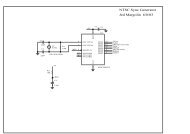
PCB SCHEMATICS<br />
U4<br />
74LVT574<br />
100Ω GND OUT_EN VCC<br />
RPAK_4<br />
2<br />
3<br />
D0<br />
D1<br />
Q0<br />
Q1<br />
1 8<br />
U8<br />
1 4<br />
5<br />
6<br />
7<br />
D2<br />
D3<br />
D4<br />
D5<br />
Q2<br />
Q3<br />
Q4<br />
Q5<br />
8<br />
U3<br />
RPAK_4 8<br />
9<br />
10<br />
GND<br />
D6<br />
D7<br />
GND Q6<br />
Q7<br />
CLOCK<br />
1<br />
U7<br />
74LVT574<br />
100Ω GND OUT_EN VCC<br />
RPAK_4<br />
2<br />
3<br />
D0<br />
D1<br />
Q0<br />
Q1<br />
1 8<br />
U6<br />
1 4<br />
5<br />
6<br />
7<br />
D2<br />
D3<br />
D4<br />
D5<br />
Q2<br />
Q3<br />
Q4<br />
Q5<br />
8<br />
U5<br />
RPAK_4 8<br />
9<br />
10<br />
GND<br />
D6<br />
D7<br />
GND Q6<br />
Q7<br />
CLOCK<br />
DB7<br />
DB6<br />
DB5<br />
DB4<br />
DB3<br />
DB2<br />
DB1<br />
DB0<br />
1<br />
E72<br />
E7<br />
E12<br />
E4<br />
E70<br />
E71<br />
DA0<br />
DA1<br />
DA2<br />
DA3<br />
DA4<br />
DA5<br />
20<br />
D3B<br />
D2B<br />
D1B<br />
D0B<br />
DRVDD<br />
DRGND<br />
D0A<br />
D1A<br />
D2A<br />
19<br />
18<br />
17<br />
16<br />
15<br />
14<br />
13<br />
12<br />
11<br />
20<br />
19<br />
18<br />
E3<br />
COUT–<br />
17<br />
16<br />
15<br />
E25<br />
DB7<br />
E15 E16<br />
E2 E1<br />
E5<br />
14<br />
13<br />
12<br />
33 32 31 30 29 28 27 26 25 24 23<br />
11<br />
VDL<br />
VDL<br />
100Ω<br />
RP1<br />
GND<br />
OUTPUT<br />
CONNECTOR<br />
1 16<br />
15<br />
14<br />
13<br />
12<br />
10<br />
9<br />
40<br />
38<br />
36<br />
34<br />
32<br />
30<br />
28<br />
26<br />
24<br />
22<br />
20<br />
18<br />
16<br />
14<br />
12<br />
10<br />
8<br />
P40<br />
P38<br />
P36<br />
P34<br />
P32<br />
P30<br />
P28<br />
P26<br />
P24<br />
P22<br />
P20<br />
P18<br />
P16<br />
P14<br />
P12<br />
P10<br />
P8<br />
P6<br />
P4<br />
P2<br />
P39<br />
P37<br />
P35<br />
P33<br />
P31<br />
P29<br />
P27<br />
P25<br />
P23<br />
P21<br />
P19<br />
P17<br />
P15<br />
P13<br />
P11<br />
P9<br />
P7<br />
P5<br />
P3<br />
P1<br />
9<br />
7<br />
5<br />
3<br />
1<br />
6<br />
4<br />
2<br />
P23<br />
39<br />
37<br />
35<br />
33<br />
31<br />
29<br />
27<br />
25<br />
23<br />
21<br />
19<br />
17<br />
15<br />
13<br />
11<br />
GND<br />
DR+<br />
GND<br />
DB7X<br />
DB6X<br />
DB5X<br />
DB4X<br />
DB3X<br />
DB2X<br />
DB1X<br />
DB0X<br />
2<br />
DB6<br />
DB5<br />
DB4<br />
3<br />
4<br />
P13 P12 P1<br />
5<br />
GND<br />
GND<br />
R2<br />
100Ω<br />
C20<br />
X<br />
COUT+<br />
R3<br />
100Ω<br />
C16<br />
X<br />
GND<br />
11<br />
DB7X<br />
DB6X<br />
DB5X<br />
DB4X<br />
DB3X<br />
DB2X<br />
DB1X<br />
DB0X<br />
6<br />
7<br />
8<br />
CLKLAT+<br />
VDL<br />
GND<br />
R40<br />
X<br />
R41<br />
X<br />
NOTE: TWO 40 PIN OUTPUT CONNECTOR<br />
IMPLEMENTED AS ONE 80 PIN CONNECTOR<br />
100Ω<br />
RP2<br />
GND<br />
OUTPUT<br />
CONNECTOR<br />
1 16<br />
15<br />
14<br />
13<br />
12<br />
10<br />
9<br />
40<br />
38<br />
36<br />
34<br />
32<br />
30<br />
28<br />
26<br />
24<br />
22<br />
20<br />
18<br />
16<br />
14<br />
12<br />
10<br />
8<br />
P40<br />
P38<br />
P36<br />
P34<br />
P32<br />
P30<br />
P28<br />
P26<br />
P24<br />
P22<br />
P20<br />
P18<br />
P16<br />
P14<br />
P12<br />
P10<br />
P8<br />
P6<br />
P4<br />
P2<br />
P39<br />
P37<br />
P35<br />
P33<br />
P31<br />
P29<br />
P27<br />
P25<br />
P23<br />
P21<br />
P19<br />
P17<br />
P15<br />
P13<br />
P11<br />
P9<br />
P7<br />
P5<br />
P3<br />
P1<br />
9<br />
7<br />
5<br />
3<br />
1<br />
6<br />
4<br />
2<br />
P3<br />
39<br />
37<br />
35<br />
33<br />
31<br />
29<br />
27<br />
25<br />
23<br />
21<br />
19<br />
17<br />
15<br />
13<br />
11<br />
GND<br />
DR–<br />
GND<br />
DA7X<br />
DA6X<br />
DA5X<br />
DA4X<br />
DA3X<br />
DA2X<br />
DA1X<br />
DA0X<br />
2<br />
3<br />
4<br />
5<br />
11<br />
DA0X<br />
DA1X<br />
DA2X<br />
DA3X<br />
DA4X<br />
DA5X<br />
DA6X<br />
DA7X<br />
6<br />
7<br />
8<br />
CLKLAT–<br />
VDL<br />
GND<br />
R38<br />
X<br />
R39<br />
X<br />
2<br />
3<br />
4<br />
2<br />
3<br />
4<br />
2<br />
3<br />
4<br />
2<br />
3<br />
4<br />
7<br />
6<br />
5<br />
7<br />
6<br />
5<br />
7<br />
6<br />
5<br />
7<br />
6<br />
5<br />
1<br />
P1<br />
2<br />
P2<br />
3<br />
P3<br />
4<br />
P4<br />
1<br />
P1<br />
2<br />
P2<br />
3<br />
P3<br />
4<br />
P4<br />
1<br />
P1<br />
2<br />
P2<br />
3<br />
P3<br />
4<br />
P4<br />
GND<br />
VAMP<br />
GND<br />
VDL<br />
GND<br />
DRVDD<br />
GND<br />
AVDD<br />
GND<br />
VCTRL<br />
GND<br />
AVDD<br />
AVDD<br />
PWDN<br />
S1<br />
GND<br />
R20<br />
XX<br />
E13 E14<br />
AVDD<br />
GND<br />
R30<br />
XX<br />
R33<br />
10kΩ<br />
SENSE<br />
AGND<br />
AVDD<br />
AVDD<br />
PWDN<br />
S1<br />
DRGND<br />
D7B<br />
D6B<br />
D5B<br />
D4B<br />
VAMP<br />
22<br />
VREF<br />
34<br />
21<br />
E19<br />
DB3<br />
DB2<br />
DB1<br />
AGND<br />
AVDD<br />
AGND<br />
35<br />
20<br />
36<br />
DB0<br />
DRVDD<br />
19<br />
37<br />
GND<br />
AVDD<br />
GND<br />
R55<br />
X<br />
18<br />
DCO+<br />
DCO–<br />
E18<br />
VIN–<br />
VIN+<br />
AGND<br />
AVDD<br />
S3<br />
DS–<br />
DS+<br />
38<br />
17<br />
39<br />
16<br />
U12<br />
<strong>AD9481</strong><br />
40<br />
GND<br />
15<br />
41<br />
DA0<br />
DA1<br />
DA2<br />
14<br />
42<br />
GND<br />
AVDD<br />
13<br />
43<br />
S3<br />
3<br />
12<br />
5<br />
44<br />
1<br />
4<br />
2<br />
6<br />
05045-040<br />
U10<br />
ADR510<br />
V+<br />
1<br />
3<br />
TRIM/NC<br />
V–<br />
2<br />
GND<br />
C12<br />
0.1µF<br />
+<br />
C13<br />
10µF<br />
C14<br />
0.1µF<br />
R1<br />
50Ω<br />
GND<br />
GND<br />
GND<br />
J4<br />
DS–<br />
E27<br />
C49<br />
0.1µF<br />
GND<br />
J2<br />
DS+<br />
CLK+<br />
CLK–<br />
AVDD<br />
AGND<br />
DRVDD<br />
DRGND<br />
D7A<br />
D6A<br />
D5A<br />
D4A<br />
D3A<br />
AMPOUT<br />
E29<br />
AMPOUT<br />
E28<br />
E26<br />
C48<br />
0.1µF<br />
C9<br />
C8<br />
R53<br />
50Ω<br />
R35<br />
50Ω<br />
GND<br />
X<br />
X<br />
1 2 3 4 5 6 7 8 9 10 11<br />
GND<br />
GND<br />
GND<br />
GND<br />
DA3<br />
DA4<br />
DA5<br />
DA6<br />
DA7<br />
R31<br />
0Ω<br />
T1–<br />
SEC<br />
PRI<br />
E30<br />
J3<br />
ANALOG<br />
INPUT<br />
AVDD<br />
GND<br />
DRVDD<br />
GND<br />
CM<br />
CM<br />
GND<br />
C10<br />
0.1µF<br />
R28<br />
X<br />
CM<br />
T1-1T<br />
T1<br />
TIN1<br />
R22<br />
50Ω C3<br />
0.1µF<br />
DA6<br />
DA7<br />
GND<br />
GND<br />
R29<br />
0Ω<br />
R21<br />
X<br />
T1+<br />
AMPIN<br />
OP AMP CONFIGURATION<br />
REMOVE C3<br />
REMOVE R29 AND R31<br />
VCTRL<br />
R16<br />
130Ω<br />
C11<br />
0.1µF<br />
E9<br />
E10<br />
AVDD<br />
GND<br />
E6<br />
C6<br />
0.1µF<br />
VCTRL<br />
VCTRL<br />
8<br />
1<br />
VCTRL<br />
VDL<br />
DRVDD<br />
AVDD<br />
AVDD<br />
DRVDD<br />
X = NOT NORMALLY POPULATED<br />
XX = NOT POPULATED, USER SELECTED<br />
E11<br />
CLK+<br />
Q<br />
J1<br />
7<br />
E8<br />
CLK<br />
CLK–<br />
Q–<br />
R VCC<br />
CLK Q<br />
100LVEL16<br />
CLKN Q<br />
VBB VEE<br />
2<br />
R52<br />
130Ω<br />
R25<br />
82Ω<br />
6<br />
3<br />
C2<br />
0.1µF<br />
R26<br />
82Ω<br />
5<br />
4<br />
R27<br />
50Ω<br />
GND<br />
C5<br />
0.1µF<br />
U11<br />
OPTIONAL TRANSFORMER<br />
T2 ETC1-1-13<br />
GND<br />
R24<br />
510Ω<br />
R23<br />
510Ω<br />
GND<br />
GND<br />
T1+<br />
1<br />
6<br />
TIN1<br />
CM<br />
2<br />
5<br />
C4<br />
0.1µF<br />
CM<br />
PADS FOR SHORTING EL16,<br />
USED IF BYPASSING EL16<br />
P14 P15<br />
GND<br />
T1–<br />
3<br />
4<br />
GND<br />
Q<br />
CLK<br />
PRI SEC<br />
P17<br />
P16<br />
Q–<br />
CLKN<br />
Figure 39. PCB Schematic (1 of 2)<br />
Rev. 0 | Page 24 of 28
<strong>AD9481</strong><br />
VDL<br />
GND<br />
VDL<br />
GND<br />
VDL<br />
GND<br />
VDL<br />
GND<br />
E56<br />
E55<br />
E53<br />
E52<br />
E50<br />
E46<br />
E49<br />
E47<br />
E54<br />
E51<br />
E45<br />
E48<br />
R9<br />
100Ω<br />
R8<br />
100Ω<br />
R6<br />
100Ω<br />
R7<br />
100Ω<br />
COUT+<br />
COUT+<br />
COUT–<br />
COUT–<br />
1<br />
2<br />
4<br />
5<br />
9<br />
10<br />
12<br />
13<br />
1A<br />
1B<br />
2A<br />
2B<br />
3A<br />
3B<br />
4A<br />
4B<br />
U2<br />
74VCX86<br />
1Y<br />
2Y<br />
3Y<br />
4Y<br />
3<br />
6<br />
8<br />
11<br />
14<br />
7<br />
R18<br />
100Ω<br />
R19<br />
50Ω<br />
R4<br />
100Ω<br />
R5<br />
50Ω<br />
PWR<br />
GND<br />
VDL<br />
GND<br />
CLKLAT+<br />
DR+<br />
CLKAT–<br />
DR–<br />
C36<br />
10µF<br />
+<br />
R54<br />
X<br />
VAMP VAMPF<br />
GND<br />
C1<br />
X<br />
VDL<br />
C32<br />
10µF<br />
GND<br />
AVDD<br />
C33<br />
10µF<br />
GND<br />
DRVDD<br />
C34<br />
10µF<br />
GND<br />
VCTRL<br />
C35<br />
10µF<br />
+ C26 C27 C28 C29<br />
0.1µF 0.1µF 0.1µF 0.1µF<br />
+ C25 C18 C24 C17<br />
0.1µF 0.1µF 0.1µF 0.1µF<br />
+ C19 C22<br />
0.1µF 0.1µF<br />
+ C15<br />
0.1µF<br />
R58<br />
X<br />
VDL<br />
AMPIN<br />
R12<br />
X<br />
C21<br />
X<br />
C23<br />
X<br />
VAMPF<br />
R37<br />
X<br />
R10<br />
X<br />
R11<br />
X<br />
PWUP<br />
RGP1<br />
INHI<br />
INLO<br />
3<br />
4<br />
1<br />
2<br />
U1<br />
AD8351<br />
10<br />
VOCM<br />
VPOS<br />
OPHI<br />
OPLO<br />
RPG2 5<br />
COMM<br />
7<br />
6<br />
9<br />
8<br />
VAMPF<br />
VAMPF<br />
GND<br />
R32<br />
X<br />
C31<br />
X<br />
R34<br />
X<br />
R17<br />
X<br />
R36<br />
X<br />
GND<br />
GND<br />
C39<br />
X<br />
C30<br />
X<br />
R56<br />
X<br />
C7<br />
X<br />
AMPOUT<br />
AMPOUT<br />
GND<br />
E24<br />
AVDD E22<br />
E23<br />
VCTRL<br />
GND<br />
C38<br />
X<br />
R57<br />
X<br />
GND<br />
C40<br />
X<br />
GND<br />
14<br />
GND<br />
1<br />
2<br />
3<br />
NC<br />
E/D<br />
GND<br />
OPTIONAL XTALS<br />
U13<br />
XO-400<br />
VCC OUT<br />
7 VEE –OUT<br />
1<br />
VCC 6 PECL6<br />
VC<br />
OUTPUTB<br />
OUTPUT<br />
8<br />
6<br />
5<br />
4<br />
GND<br />
R14<br />
X<br />
R15<br />
X<br />
X = NOT NORMALLY POPULATED<br />
XX = NOT POPULATED, USER SELECTED<br />
R60<br />
X<br />
R51<br />
XX<br />
GND<br />
R48<br />
X<br />
R49<br />
X<br />
CLK–<br />
CLK+<br />
05045-041<br />
VCTRL<br />
R42<br />
1kΩ<br />
R43<br />
1kΩ<br />
R13<br />
1kΩ<br />
GND<br />
E35 E36<br />
E32 E39<br />
E33 E38<br />
E34 E37<br />
S1<br />
VCTRL<br />
R45<br />
X<br />
R46<br />
X<br />
GND<br />
E20 E21<br />
VCTRL PWDN<br />
AVDD<br />
GND<br />
E88<br />
S3<br />
E90<br />
E89<br />
R44<br />
1kΩ<br />
VCTRL<br />
VCTRL<br />
R59<br />
X<br />
R50<br />
XX<br />
VCTRL<br />
GND<br />
Figure 40. PCB Schematic (2 of 2)<br />
Rev. 0 | Page 25 of 28
<strong>AD9481</strong><br />
PCB LAYERS<br />
August 3, 2004<br />
05045-042<br />
05045-044<br />
Figure 41. PCB Top-Side Silkscreen<br />
Figure 43. PCB Ground Layer<br />
Figure 42. PCB Top-Side Copper Routing<br />
05045-043<br />
Figure 44. PCB Split Power Plane<br />
05045-045<br />
Rev. 0 | Page 26 of 28
<strong>AD9481</strong><br />
Figure 45. PCB Bottom-Side Copper Routing<br />
05045-046<br />
Figure 46. PCB Bottom-Side Silkscreen<br />
05045-047<br />
Rev. 0 | Page 27 of 28
<strong>AD9481</strong><br />
OUTLINE DIMENSIONS<br />
1.20<br />
MAX<br />
12.00 SQ<br />
0.75<br />
0.60<br />
0.45<br />
44<br />
34<br />
1 33<br />
PIN 1<br />
TOP VIEW<br />
(PINS DOWN)<br />
10.00<br />
SQ<br />
1.05<br />
1.00<br />
0.95<br />
0.15<br />
0.05<br />
SEATING<br />
PLANE<br />
0° MIN<br />
VIEW A<br />
ROTATED 90° CCW<br />
0.20<br />
0.09<br />
VIEW A<br />
7°<br />
3.5°<br />
0°<br />
0.08 MAX<br />
COPLANARITY<br />
11<br />
12<br />
0.80<br />
BSC<br />
0.45<br />
0.37<br />
0.30<br />
22<br />
23<br />
COMPLIANT TO JEDEC STANDARDS MS-026ACB<br />
Figure 47. 44-Lead Thin Plastic Quad Flat Package [TQFP] (SU-44)—Dimensions shown in millimeters<br />
ORDERING GUIDE<br />
Model Temperature Range Package Description Package Option<br />
<strong>AD9481</strong>BSUZ-<strong>250</strong> 1 –40°C to +85°C 44-Lead Thin Plastic Quad Flat Package (TQFP) SU-44<br />
<strong>AD9481</strong>-PCB 2 Evaluation Board<br />
1<br />
Z = Pb-free part.<br />
2<br />
Evaluation board shipped with <strong>AD9481</strong>BSUZ-<strong>250</strong> installed.<br />
© 2004 <strong>Analog</strong> <strong>Devices</strong>, Inc. All rights reserved. Trademarks and<br />
registered trademarks are the property of their respective owners.<br />
D05045–0–10/04(0)<br />
Rev. 0 | Page 28 of 28