c-Si PVMC Brief Overview
c-Si PVMC Brief Overview
c-Si PVMC Brief Overview

Create successful ePaper yourself
Turn your PDF publications into a flip-book with our unique Google optimized e-Paper software.
c‐<strong>Si</strong> <strong>PVMC</strong> <strong>Brief</strong> <strong>Overview</strong><br />
Intersolar NA –San Francisco, CA<br />
Dr. Winston V. Schoenfeld<br />
Director, c‐<strong>Si</strong> PVCM<br />
July 10 th , 2012<br />
The data contained in all slides of this presentation is protected data produced under agreement no. DE‐EE0004947 with the<br />
U.S. Department of Energy and may not be published, disseminated, or disclosed to others outside the Government until five (5)<br />
years from the date the data was produced, unless express written authorization is obtained from the recipient. Upon<br />
expiration of the period of protection set forth in this Notice, the Government shall have unlimited rights in this data. This<br />
Notice shall be marked on any reproduction of this data, in whole or in part.
DOE SunShot Initiative<br />
• Mission of DOE SunShot Initiative<br />
- Deliver grid-parity solar PV by 2020, a goal that will demand<br />
~75% reduction in the cost of systems compared with today<br />
- Restore US leadership in the global clean energy race<br />
• SunShot Photovoltaic Manufacturing Initiative (PVMI) - $110M<br />
• PV Cells / Modules – 3 recipients<br />
Balance of System<br />
Power Electronics<br />
• April 2011 – award recipients of solar cell/module<br />
- Industry-led consortium, SEMATECH – <strong>PVMC</strong><br />
Copper indium gallium selenide (CIGS) pilot line, in partnership with CNSE<br />
c-<strong>Si</strong> metrology and feedstock/wafering technologies, in partnership with UCF/FSEC in Florida<br />
- PV manufacturing development facility – SVTC<br />
- University-led consortium – BAPVC (Stanford/Berkeley)<br />
U.S. Photovoltaic Manufacturing Consortium (<strong>PVMC</strong>)<br />
Consortium<br />
Management<br />
CIGS<br />
c‐<strong>Si</strong><br />
2
c‐<strong>Si</strong> <strong>PVMC</strong> Program Areas<br />
& Structure
Initial c‐<strong>Si</strong> <strong>PVMC</strong> Program Areas<br />
1. In‐line/Off‐line Metrology<br />
Primary Goals<br />
– Identify critical industry challenges/needs in metrology and rank<br />
– Participate and support c‐<strong>Si</strong> standards development and roadmapping efforts<br />
– Develop projects to demonstrate new c‐<strong>Si</strong> metrology technologies<br />
– Build infrastructure to support metrology programs<br />
– Transition new metrology technologies into pilot and manufacturing lines<br />
Courtesy of Polaritek<br />
2. New Feedstock/Wafering Methodologies<br />
Primary Goals<br />
– Identify critical industry needs in feedstock and metrology<br />
Courtesy of AMAT<br />
– Establish c‐<strong>Si</strong> feedstock/wafering programs to accelerate transition of new technologies into mainstream manufacturing<br />
– Provide/foster process, test, and demonstration activities to validate new technologies and identify barriers<br />
– Participate and support c‐<strong>Si</strong> standards development and roadmapping efforts
The c‐<strong>Si</strong> <strong>PVMC</strong> Organizational Structure<br />
‐ Oversight of all c‐<strong>Si</strong> <strong>PVMC</strong> programs and personnel<br />
‐ Strategic planning and expansion<br />
‐ Management of program areas<br />
‐ Coordination of program area<br />
activities<br />
Program Area Oversight<br />
‐ Sets Program Area priorities<br />
‐ Selects consortium projects and resource allocation<br />
‐ Reviews program area directions/deliverables/milestones<br />
‐ Populated by Consortium Members<br />
Project Area Oversight<br />
‐ Identifies potential Program Area projects<br />
‐ Ranks potential Projects through Pareto analysis<br />
‐ Sets Project goals/metrics/deliverables<br />
‐ Carries out Project tasks, populated with Assignees<br />
‐ Leads Roadmapping and Standards Development<br />
Key Point: Programs are initiated, monitored, and measured by <strong>PVMC</strong> members
c‐<strong>Si</strong> <strong>PVMC</strong> Activities Timeline<br />
Identify Challenges<br />
Identify Projects<br />
Select<br />
Projects
c‐<strong>Si</strong> Challenges Pareto Results<br />
Identify Challenges<br />
Identify Projects<br />
Select<br />
Projects
c‐<strong>Si</strong> <strong>PVMC</strong> Challenges Pareto Effort<br />
Code<br />
W-C1<br />
W-C2<br />
W-C3<br />
W-C4<br />
Wafer Production Area Challenges<br />
Thin wafers handling and processing (e.g. limiting breakage); Thin wafer<br />
interconnection; Test methods or a specific handling target to<br />
characterizate/validate handling for thin wafers; Pre-processing, handling, and<br />
packaging/shipment of thin wafers to cell manufacturer<br />
Slurry recycling<br />
Reduction of kerf loss<br />
Unified incoming wafer specifications and standards; Better specifications for<br />
mechanical and electrical characterization (Affects cell effiency & end product<br />
performance)<br />
Grain boundary passivation of multicrystalline <strong>Si</strong> wafers<br />
W-C5<br />
W-C6 Determination of electrical activity of crystallographic defects in a wafer<br />
W-C7 Understanding critical crack lengths vs. wafer thickness<br />
W-C8 Wafer consistancy<br />
Lack of detailed information from customers (only pass/fail info given); Lack of<br />
W-C9<br />
US based solar companies for partnerships<br />
W-C10 Saw damage removal and surface characterization<br />
New wafering technologies (kerf-free, implan/cleave, direct wafer technology ,<br />
W-C11<br />
etc.); Lower cost SOI wafers<br />
W-C12 Correlation of reliability/degradation mechanisms to wafer quality/properties<br />
Decoupling bulk and surface recombination in carrier lifetime measurement;<br />
W-C13 Carrier lifetime measurements at the wafer level, better prediction of cell<br />
efficency<br />
In-line inspection of wafers; Determine optimal scan density and cost versus<br />
W-C14<br />
need (value-cost curve)<br />
Unknown impact of new wafer formats (ex. quasi-mono wafers, n-type wafers,<br />
W-C15<br />
etc.) on cleaning and texturing processes<br />
<strong>PVMC</strong> Confidential –Not for reproduction/distribution without written permission from <strong>PVMC</strong>‐FL
c‐<strong>Si</strong> Potential Projects Pareto Results –<br />
Effort undertaken after Challenges<br />
Pareto<br />
Identify Challenges<br />
Identify Projects<br />
Select<br />
Projects
M‐P1<br />
Goals and Main<br />
Objectives<br />
Expected Duration<br />
Challenge Addressed<br />
<strong>Brief</strong> Description<br />
Example Metrology Project Description<br />
Improved methods of characterizing mechanical integrity of wafers/cells and<br />
identifying wafers that might lead to high breakage<br />
• More reliably detect what wafers/cells might lead to cracks before, during and<br />
after processing (i.e. go/no‐go criteria)<br />
• Gain further understanding of the key process steps and handling issues that<br />
induce cracks (externally applied stress)<br />
• Improve accuracy and reliability of residual stress/strain and crack detection<br />
measurements for various sample types<br />
• Develop in‐line methods for measuring elastic properties of wafers/cells<br />
• Improved manufacturing yield for thin and standard thickness wafers/cells<br />
• Potential β‐site demonstration of in‐line cell metrology tool(s)<br />
2‐3 years<br />
Primary: W‐C1, W‐C7, FW‐C7, FW‐C8, C‐C1, M‐C8, MCC‐C7, MCC‐C10<br />
Secondary: W‐C4, W‐C12, W‐C14, FCC‐C5, C‐C6, C‐C12, MCC‐C4, MCC‐C8<br />
A statistically relevant number of incoming wafers (thin and standard thickness) are<br />
processed in lots with various process parameters and handling methods, with in‐line<br />
measurements (RUV, optical) performed at various points (beforehand and during<br />
critical process/handling steps). Failures are inspected using established off‐line<br />
methods (SAM, X‐ray based, optical, Kelvin probe). Stress tests (thermal cycling,<br />
mechanical impact, test‐to‐failure methods) are carried out on cells along with<br />
additional characterization. Models are developed and refined to provide go/no‐go<br />
criteria for breakage. A smaller sample size of wafers is fully characterized before,<br />
during and after processing to more thoroughly investigate the evolution of the<br />
stress/strain profiles throughout processing and refine models.<br />
Challenges in RED were among top three challenges for that production area.<br />
<strong>PVMC</strong> Confidential –Not for reproduction/distribution without written permission from <strong>PVMC</strong>
c‐<strong>Si</strong> <strong>PVMC</strong> Potential Projects Pareto Effort<br />
<strong>PVMC</strong> Confidential –Not for reproduction/distribution without written permission from <strong>PVMC</strong>
c‐<strong>Si</strong> <strong>PVMC</strong> Membership<br />
Identify Challenges<br />
Identify Projects<br />
Select<br />
Projects
Membership Process Timeline
c‐<strong>Si</strong> <strong>PVMC</strong> Membership Levels<br />
Two Membership Levels:<br />
– Full Members<br />
• TAB seat in both Program Areas<br />
• Working Group Participation<br />
• Access to/participation in all Program Areas (Metrology,<br />
Feedstock/Wafering, etc.)<br />
• Full IP access<br />
– Program Members<br />
• TAB Participation in designated Program Area (Designated in Attachment<br />
A of Participant Agreement)<br />
• Working Group Participation in designated Program Area<br />
• Access to/participation in designated Program Area<br />
• IP access within designated Program Area
c‐<strong>Si</strong> <strong>PVMC</strong> Calendar of Events
2012 c‐<strong>Si</strong> US <strong>PVMC</strong> Events Calendar<br />
Date Event Format Amplification<br />
JAN 1/11 and 1/12 Kick-off meetings WebEx/telecon Identify/list key challenges<br />
FEB<br />
2/1 and 2/2 Follow-up Meetings WebEx/telecon Review Pareto results for challenges<br />
2/7/2012 Conference - Washington, DC DOE Metrology Workshop Networking<br />
MAR 3/7 and 3/8 Working Group Face to face meeting Identify projects for Pareto analysis<br />
4/12/2012 Working Group WebEx/telecon Review Pareto and provide comments<br />
APR<br />
NREL-<strong>PVMC</strong> Projects<br />
4/25/2012 John Wohlgemuth - NREL WebEx/telecon<br />
Review Papers/Standards<br />
5/3/2012 SEMATECH-<strong>PVMC</strong> Meeting Face to face meeting Progress Status<br />
MAY<br />
5/7/2012 Carl Osterwald - NREL WebEx/telecon Standards<br />
5/8/2012 Larry Sherwood – Solar ABCs WebEx/telecon Standards<br />
5/25/2012 Workshop Committee WebEx/telecon Select Technical Program<br />
JUN<br />
6/6/2012<br />
Standards kick-off meetings<br />
Conference - Austin, TX<br />
IEEE PVSC<br />
5pm – 8:30pm<br />
Networking<br />
Working Group WebEx/telecon Project execution and review<br />
6/13 and 6/14<br />
DOE Forum Poster session Showcase c-<strong>Si</strong> <strong>PVMC</strong><br />
7/10<br />
Feedstock/Wafering Workshop<br />
7/11 Conference – San Francisco, CA<br />
Intersolar NA<br />
Networking<br />
7/12<br />
Metrology Workshop<br />
JUL<br />
7/25/12<br />
Conference - Vail, CO<br />
Roadmap kick-off meeting<br />
7/25/12<br />
NREL c-<strong>Si</strong> Workshop<br />
Networking<br />
7/26/12<br />
Golden, CO<br />
NREL Visit<br />
AUG 8/8 and 8/9 Working Group WebEx/telecon Project execution and review<br />
9/10/12<br />
Face to face meetings<br />
SEP to<br />
Conference - Orlando, FL Solar Power International<br />
SDOs Forum<br />
9/13/12<br />
Networking<br />
OCT 10/10 and 10/11 Working Group WebEx/telecon Project execution and review<br />
NOV 11/14 and 11/15 Working Group WebEx/telecon Project execution and review<br />
DEC 12/12 and 12/13 Working Group WebEx/telecon Project execution and review
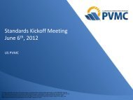
c‐<strong>Si</strong> <strong>PVMC</strong> Standards Kick‐off Meeting<br />
IEEE PVSC – Austin, TX – Wednesday 6/7/2012 5pm – 8:30pm<br />
• Q: How can we better integrate c‐<strong>Si</strong> US<strong>PVMC</strong> standard efforts with<br />
existing SDO activities –What is its role?<br />
– c‐<strong>Si</strong> <strong>PVMC</strong> Role: Participate, not re‐create!<br />
– Invited representatives from SDOs to participate<br />
• >30 Participant Attended/Actively Participated<br />
– SEMI, IEC, ASTM, Solar ABCs, NREL, UL, and Industry<br />
• Discussion Topics<br />
– <strong>Overview</strong> of existing SDOs/WGs/TFs/standards potentially<br />
related to c‐<strong>Si</strong> <strong>PVMC</strong> Programs<br />
– Identify gaps in standards that c‐<strong>Si</strong> <strong>PVMC</strong> can facilitate<br />
– Identify specific ways c‐<strong>Si</strong> <strong>PVMC</strong> can engage w/ SDOs
c‐<strong>Si</strong> Report Generated to Document Findings/AIs<br />
• Documents attendees, discussions, findings, and action items.
c‐<strong>Si</strong> <strong>PVMC</strong> Roadmaps Kick‐off Meeting<br />
NREL c‐<strong>Si</strong> Workshop at Vail, CO<br />
Wednesday 7/25/2012 1pm –4pm<br />
• Identify and discuss existing c‐<strong>Si</strong> roadmaps<br />
– Which ones are out there?<br />
– Who owns them?<br />
• Do they cover the two program areas appropriately? Identify<br />
potential gaps/needs<br />
• Discuss what elements are key in making a roadmap attractive<br />
to the industry so that it is accepted and embraced by<br />
industry