Octal Bus Transceivers With 3-State Outputs (Rev. A)
Octal Bus Transceivers With 3-State Outputs (Rev. A)
Octal Bus Transceivers With 3-State Outputs (Rev. A)

You also want an ePaper? Increase the reach of your titles
YUMPU automatically turns print PDFs into web optimized ePapers that Google loves.
3-<strong>State</strong> <strong>Outputs</strong> Drive <strong>Bus</strong> Lines Directly<br />
PNP Inputs Reduce dc Loading on <strong>Bus</strong><br />
Lines<br />
Hysteresis at <strong>Bus</strong> Inputs Improves Noise<br />
Margins<br />
Typical Propagation Delay Times Port to<br />
Port, 8 ns<br />
TYPE<br />
IOL<br />
(SINK<br />
CURRENT)<br />
IOH<br />
(SOURCE<br />
CURRENT)<br />
SN54LS245 12 mA –12 mA<br />
SN74LS245 24 mA –15 mA<br />
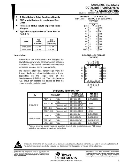
SN54LS245, SN74LS245<br />
OCTAL BUS TRANSCEIVERS<br />
WITH 3-STATE OUTPUTS<br />
SDLS146A – OCTOBER 1976 – REVISED FEBRUARY 2002<br />
SN54LS245 ...J OR W PACKAGE<br />
SN74LS245 ... DB, DW, N, OR NS PACKAGE<br />
(TOP VIEW)<br />
DIR<br />
A1<br />
A2<br />
A3<br />
A4<br />
A5<br />
A6<br />
A7<br />
A8<br />
GND<br />
1<br />
2<br />
3<br />
4<br />
5<br />
6<br />
7<br />
8<br />
9<br />
10<br />
20<br />
19<br />
18<br />
17<br />
16<br />
15<br />
14<br />
13<br />
12<br />
11<br />
V CC<br />
OE<br />
B1<br />
B2<br />
B3<br />
B4<br />
B5<br />
B6<br />
B7<br />
B8<br />
description<br />
These octal bus transceivers are designed for<br />
asynchronous two-way communication between<br />
data buses. The control-function implementation<br />
minimizes external timing requirements.<br />
The devices allow data transmission from the<br />
A bus to the B bus or from the B bus to the A bus,<br />
depending on the logic level at the<br />
direction-control (DIR) input. The output-enable<br />
(OE) input can disable the device so that the<br />
buses are effectively isolated.<br />
SN54LS245 . . . FK PACKAGE<br />
(TOP VIEW)<br />
A3<br />
A4<br />
A5<br />
A6<br />
A7<br />
A2<br />
A1<br />
DIR<br />
B8<br />
B7<br />
V CC<br />
B6 OE<br />
3<br />
4<br />
2 1 20 19<br />
18<br />
5<br />
6<br />
7<br />
17<br />
16<br />
15<br />
8<br />
14<br />
9 10 11 12 13<br />
A8<br />
GND<br />
B1<br />
B2<br />
B3<br />
B4<br />
B5<br />
TA<br />
0°C to 70°C<br />
–55°C to125°C<br />
ORDERING INFORMATION<br />
PACKAGE†<br />
ORDERABLE<br />
PART NUMBER<br />
TOP-SIDE<br />
MARKING<br />
PDIP – N Tube SN74LS245N SN74LS245N<br />
SOIC – DW<br />
Tube<br />
Tape and reel<br />
SN74LS245DW<br />
SN74LS245DWR<br />
LS245<br />
SOP – NS Tape and reel SN74LS245NSR 74LS245<br />
SSOP – DB Tape and reel SN74LS245DBR LS245<br />
CDIP – J<br />
Tube SN54LS245J SN54LS245J<br />
Tube SNJ54LS245J SNJ54LS245J<br />
CFP – W Tube SNJ54LS245W SNJ54LS245W<br />
LCCC – FK Tube SN54LS245FK SN54LS245FK<br />
† Package drawings, standard packing quantities, thermal data, symbolization, and PCB design<br />
guidelines are available at www.ti.com/sc/package.<br />
Please be aware that an important notice concerning availability, standard warranty, and use in critical applications of<br />
Texas Instruments semiconductor products and disclaimers thereto appears at the end of this data sheet.<br />
PRODUCTION DATA information is current as of publication date.<br />
Products conform to specifications per the terms of Texas Instruments<br />
standard warranty. Production processing does not necessarily include<br />
testing of all parameters.<br />
Copyright © 2002, Texas Instruments Incorporated<br />
On products compliant to MIL-PRF-38535, all parameters are tested<br />
unless otherwise noted. On all other products, production<br />
processing does not necessarily include testing of all parameters.<br />
POST OFFICE BOX 655303 • DALLAS, TEXAS 75265<br />
1
SN54LS245, SN74LS245<br />
OCTAL BUS TRANSCEIVERS<br />
WITH 3-STATE OUTPUTS<br />
SDLS146A – OCTOBER 1976 – REVISED FEBRUARY 2002<br />
FUNCTION TABLE<br />
INPUTS<br />
OE DIR<br />
OPERATION<br />
L L B data to A bus<br />
L H A data to B bus<br />
H X Isolation<br />
schematics of inputs and outputs<br />
EQUIVALENT OF EACH INPUT<br />
TYPICAL OF ALL OUTPUTS<br />
VCC<br />
VCC<br />
9 kΩ NOM<br />
50 Ω NOM<br />
Input<br />
Output<br />
logic diagram (positive logic)<br />
DIR<br />
1<br />
19<br />
OE<br />
A1<br />
2<br />
18<br />
B1<br />
To Seven Other Channels<br />
2 POST OFFICE BOX 655303 • DALLAS, TEXAS 75265
SN54LS245, SN74LS245<br />
OCTAL BUS TRANSCEIVERS<br />
WITH 3-STATE OUTPUTS<br />
SDLS146A – OCTOBER 1976 – REVISED FEBRUARY 2002<br />
absolute maximum ratings over operating free-air temperature range (unless otherwise noted) †<br />
Supply voltage, V CC . . . . . . . . . . . . . . . . . . . . . . . . . . . . . . . . . . . . . . . . . . . . . . . . . . . . . . . . . . . . . . . . . . . . . . . . 7 V<br />
Input voltage, V I (see Note 1) . . . . . . . . . . . . . . . . . . . . . . . . . . . . . . . . . . . . . . . . . . . . . . . . . . . . . . . . . . . . . . . . . 7 V<br />
Package thermal impedance, JA (see Note 2): DB package . . . . . . . . . . . . . . . . . . . . . . . . . . . . . . . . . 70°C/W<br />
DW package . . . . . . . . . . . . . . . . . . . . . . . . . . . . . . . . 58°C/W<br />
N package . . . . . . . . . . . . . . . . . . . . . . . . . . . . . . . . . . 69°C/W<br />
NS package . . . . . . . . . . . . . . . . . . . . . . . . . . . . . . . . . 60°C/W<br />
Storage temperature range, T stg . . . . . . . . . . . . . . . . . . . . . . . . . . . . . . . . . . . . . . . . . . . . . . . . . . . –65°C to 150°C<br />
† Stresses beyond those listed under “absolute maximum ratings” may cause permanent damage to the device. These are stress ratings only, and<br />
functional operation of the device at these or any other conditions beyond those indicated under “recommended operating conditions” is not<br />
implied. Exposure to absolute-maximum-rated conditions for extended periods may affect device reliability.<br />
NOTES: 1. All voltage values are with respect to GND.<br />
2. The package thermal impedance is calculated in accordance with JESD 51-7.<br />
recommended operating conditions<br />
SN54LS245<br />
SN74LS245<br />
MIN NOM MAX MIN NOM MAX<br />
VCC Supply voltage 4.5 5 5.5 4.75 5 5.25 V<br />
IOH High-level output current –12 –15 mA<br />
IOL Low-level output current 12 24 mA<br />
TA Operating free-air temperature –55 125 0 70 °C<br />
UNIT<br />
POST OFFICE BOX 655303 • DALLAS, TEXAS 75265<br />
3
SN54LS245, SN74LS245<br />
OCTAL BUS TRANSCEIVERS<br />
WITH 3-STATE OUTPUTS<br />
SDLS146A – OCTOBER 1976 – REVISED FEBRUARY 2002<br />
electrical characteristics over recommended operating free-air temperature range (unless<br />
otherwise noted)<br />
PARAMETER<br />
TEST CONDITIONS†<br />
SN54LS245<br />
SN74LS245<br />
MIN TYP‡ MAX MIN TYP‡ MAX<br />
VIH High-level input voltage 2 2 V<br />
VIL Low-level input voltage 0.7 0.8 V<br />
VIK Input clamp voltage VCC = MIN, II = –18 mA –1.5 –1.5 V<br />
Hysteresis (VT+ – VT–) A or B VCC = MIN 0.2 0.4 0.2 0.4 V<br />
VCC = MIN,<br />
VOH High-level output voltage VIH = 2V<br />
V,<br />
VIL = VIL(max)<br />
VCC = MIN,<br />
VOL Low-level output voltage VIH = 2V<br />
V,<br />
VIL = VIL(max)<br />
IOZH<br />
IOZL<br />
II<br />
Off-state output current,<br />
high-level voltage applied<br />
Off-state output current,<br />
low-level voltage applied<br />
Input current at<br />
maximum input<br />
voltage<br />
A or B<br />
DIR or OE<br />
VCC = MAX,<br />
OE at 2 V<br />
VCC = MAX,<br />
OE at 2 V<br />
VCC = MAX<br />
IOH = –3 mA 2.4 3.4 2.4 3.4<br />
IOH = MAX 2 2<br />
IOL = 12 mA 0.4 0.4<br />
IOL = 24 mA 0.5<br />
UNIT<br />
VO = 2.7 V 20 20 µA<br />
VO = 0.4 V –200 –200 µA<br />
VI = 5.5 V 0.1 0.1<br />
VI = 7 V 0.1 0.1<br />
IIH High-level input current VCC = MAX, VIH = 2.7 V 20 20 µA<br />
IIL Low-level input current VCC = MAX, VIL = 0.4 V –0.2 –0.2 mA<br />
IOS Short-circuit output current§ VCC = MAX –40 –225 40 –225 mA<br />
Total, outputs high 48 70 48 70<br />
ICC Supply current Total, outputs low VCC = MAX <strong>Outputs</strong> open 62 90 62 90 mA<br />
<strong>Outputs</strong> at high Z 64 95 64 95<br />
† For conditions shown as MIN or MAX, use the appropriate values specified under recommended operating conditions.<br />
‡ All typical values are at VCC = 5 V, TA = 25°C.<br />
§ Not more than one output should be shorted at a time, and duration of the short circuit should not exceed one second.<br />
switching characteristics, V CC = 5 V, T A = 25°C (see Figure 1)<br />
PARAMETER TEST CONDITIONS MIN TYP MAX UNIT<br />
tPLH Propagation delay time, low- to high-level output<br />
8 12<br />
CL = 45 pF,<br />
RL = 667 <br />
tPHL Propagation delay time, high- to low-level level output 8 12<br />
tPZL<br />
tPZH<br />
tPLZ<br />
tPHZ<br />
Output enable time to low level<br />
Output enable time to high level<br />
Output disable time from low level<br />
Output disable time from high level<br />
CL =45pF<br />
pF,<br />
CL =5pF<br />
pF,<br />
RL = 667 <br />
RL = 667 <br />
27 40<br />
25 40<br />
15 25<br />
15 28<br />
V<br />
V<br />
mA<br />
ns<br />
ns<br />
ns<br />
4 POST OFFICE BOX 655303 • DALLAS, TEXAS 75265
PARAMETER MEASUREMENT INFORMATION<br />
SERIES 54LS/74LS DEVICES<br />
SN54LS245, SN74LS245<br />
OCTAL BUS TRANSCEIVERS<br />
WITH 3-STATE OUTPUTS<br />
SDLS146A – OCTOBER 1976 – REVISED FEBRUARY 2002<br />
From Output<br />
Under Test<br />
Test<br />
Point<br />
CL<br />
(see Note A)<br />
VCC<br />
RL<br />
(see Note B)<br />
From Output<br />
Under Test<br />
CL<br />
(see Note A)<br />
VCC<br />
RL<br />
Test<br />
Point<br />
VCC<br />
From Output<br />
Under Test<br />
CL<br />
(see Note A)<br />
Test<br />
Point<br />
RL<br />
5 kΩ<br />
S1<br />
(see Note B)<br />
S2<br />
LOAD CIRCUIT<br />
FOR 2-STATE TOTEM-POLE OUTPUTS<br />
LOAD CIRCUIT<br />
FOR OPEN-COLLECTOR OUTPUTS<br />
LOAD CIRCUIT<br />
FOR 3-STATE OUTPUTS<br />
High-Level<br />
Pulse<br />
Low-Level<br />
Pulse<br />
1.3 V 1.3 V<br />
tw<br />
1.3 V 1.3 V<br />
VOLTAGE WAVEFORMS<br />
PULSE DURATIONS<br />
Timing<br />
Input<br />
Data<br />
Input<br />
tsu<br />
1.3 V<br />
th<br />
1.3 V 1.3 V<br />
VOLTAGE WAVEFORMS<br />
SETUP AND HOLD TIMES<br />
3 V<br />
0 V<br />
3 V<br />
0 V<br />
Input<br />
1.3 V 1.3 V<br />
3 V<br />
0 V<br />
Output<br />
Control<br />
(low-level<br />
enabling)<br />
tPZL<br />
1.3 V 1.3 V<br />
tPLZ<br />
3 V<br />
0 V<br />
In-Phase<br />
Output<br />
(see Note D)<br />
Out-of-Phase<br />
Output<br />
(see Note D)<br />
tPLH<br />
tPHL<br />
VOLTAGE WAVEFORMS<br />
PROPAGATION DELAY TIMES<br />
tPHL<br />
1.3 V 1.3 V<br />
tPLH<br />
1.3 V 1.3 V<br />
VOH<br />
VOL<br />
VOH<br />
VOL<br />
Waveform 1<br />
(see Notes C<br />
and D)<br />
Waveform 2<br />
(see Notes C<br />
and D)<br />
NOTES: A. CL includes probe and jig capacitance.<br />
B. All diodes are 1N3064 or equivalent.<br />
C. Waveform 1 is for an output with internal conditions such that the output is low except when disabled by the output control.<br />
Waveform 2 is for an output with internal conditions such that the output is high except when disabled by the output control.<br />
D. S1 and S2 are closed for tPLH, tPHL, tPHZ, and tPLZ; S1 is open and S2 is closed for tPZH; S1 is closed and S2 is open for tPZL.<br />
E. Phase relationships between inputs and outputs have been chosen arbitrarily for these examples.<br />
F. All input pulses are supplied by generators having the following characteristics: PRR ≤ 1 MHz, ZO ≈ 50 Ω, tr ≤ 1.5 ns, tf ≤ 2.6 ns.<br />
G. The outputs are measured one at a time with one input transition per measurement.<br />
tPZH<br />
1.3 V<br />
Figure 1. Load Circuits and Voltage Waveforms<br />
1.3 V<br />
tPHZ<br />
≈1.5 V<br />
VOL + 0.5 V<br />
VOL<br />
VOH<br />
VOH – 0.5 V<br />
≈1.5 V<br />
VOLTAGE WAVEFORMS<br />
ENABLE AND DISABLE TIMES, 3-STATE OUTPUTS<br />
POST OFFICE BOX 655303 • DALLAS, TEXAS 75265<br />
5
PACKAGE OPTION ADDENDUM<br />
www.ti.com<br />
29-Aug-2012<br />
PACKAGING INFORMATION<br />
Orderable Device Status (1) Package Type Package<br />
Drawing<br />
Pins Package Qty Eco Plan (2) Lead/<br />
Ball Finish<br />
MSL Peak Temp (3)<br />
5962-8002101VRA ACTIVE CDIP J 20 20 TBD A42 N / A for Pkg Type<br />
5962-8002101VSA ACTIVE CFP W 20 1 TBD Call TI N / A for Pkg Type<br />
80021012A ACTIVE LCCC FK 20 1 TBD Call TI Call TI<br />
8002101SA ACTIVE CFP W 20 1 TBD Call TI Call TI<br />
JM38510/32803B2A ACTIVE LCCC FK 20 1 TBD POST-PLATE N / A for Pkg Type<br />
JM38510/32803BRA ACTIVE CDIP J 20 1 TBD A42 N / A for Pkg Type<br />
JM38510/32803BSA ACTIVE CFP W 20 1 TBD Call TI N / A for Pkg Type<br />
M38510/32803B2A ACTIVE LCCC FK 20 1 TBD POST-PLATE N / A for Pkg Type<br />
M38510/32803BRA ACTIVE CDIP J 20 1 TBD A42 N / A for Pkg Type<br />
M38510/32803BSA ACTIVE CFP W 20 1 TBD Call TI N / A for Pkg Type<br />
SN54LS245J ACTIVE CDIP J 20 1 TBD A42 N / A for Pkg Type<br />
SN74LS245DBR ACTIVE SSOP DB 20 2000 Green (RoHS<br />
& no Sb/Br)<br />
SN74LS245DBRE4 ACTIVE SSOP DB 20 2000 Green (RoHS<br />
& no Sb/Br)<br />
SN74LS245DBRG4 ACTIVE SSOP DB 20 2000 Green (RoHS<br />
& no Sb/Br)<br />
SN74LS245DW ACTIVE SOIC DW 20 25 Green (RoHS<br />
& no Sb/Br)<br />
SN74LS245DWG4 ACTIVE SOIC DW 20 25 Green (RoHS<br />
& no Sb/Br)<br />
SN74LS245DWR ACTIVE SOIC DW 20 2000 Green (RoHS<br />
& no Sb/Br)<br />
SN74LS245DWRG4 ACTIVE SOIC DW 20 2000 Green (RoHS<br />
& no Sb/Br)<br />
CU NIPDAU<br />
CU NIPDAU<br />
CU NIPDAU<br />
CU NIPDAU<br />
CU NIPDAU<br />
CU NIPDAU<br />
CU NIPDAU<br />
SN74LS245J OBSOLETE CDIP J 20 TBD Call TI Call TI<br />
Level-1-260C-UNLIM<br />
Level-1-260C-UNLIM<br />
Level-1-260C-UNLIM<br />
Level-1-260C-UNLIM<br />
Level-1-260C-UNLIM<br />
Level-1-260C-UNLIM<br />
Level-1-260C-UNLIM<br />
SN74LS245N ACTIVE PDIP N 20 20 Pb-Free (RoHS) CU NIPDAU N / A for Pkg Type<br />
SN74LS245N3 OBSOLETE PDIP N 20 TBD Call TI Call TI<br />
SN74LS245NE4 ACTIVE PDIP N 20 20 Pb-Free (RoHS) CU NIPDAU N / A for Pkg Type<br />
SN74LS245NSR ACTIVE SO NS 20 2000 Green (RoHS<br />
& no Sb/Br)<br />
CU NIPDAU Level-1-260C-UNLIM<br />
Samples<br />
(Requires Login)<br />
Addendum-Page 1
PACKAGE OPTION ADDENDUM<br />
www.ti.com<br />
29-Aug-2012<br />
Orderable Device Status (1) Package Type Package<br />
Drawing<br />
Pins Package Qty Eco Plan (2) Lead/<br />
Ball Finish<br />
SN74LS245NSRE4 ACTIVE SO NS 20 2000 Green (RoHS<br />
& no Sb/Br)<br />
SN74LS245NSRG4 ACTIVE SO NS 20 2000 Green (RoHS<br />
& no Sb/Br)<br />
CU NIPDAU<br />
CU NIPDAU<br />
MSL Peak Temp (3)<br />
Level-1-260C-UNLIM<br />
Level-1-260C-UNLIM<br />
SNJ54LS245FK ACTIVE LCCC FK 20 1 TBD POST-PLATE N / A for Pkg Type<br />
SNJ54LS245J ACTIVE CDIP J 20 1 TBD A42 N / A for Pkg Type<br />
SNJ54LS245W ACTIVE CFP W 20 1 TBD Call TI N / A for Pkg Type<br />
Samples<br />
(Requires Login)<br />
(1) The marketing status values are defined as follows:<br />
ACTIVE: Product device recommended for new designs.<br />
LIFEBUY: TI has announced that the device will be discontinued, and a lifetime-buy period is in effect.<br />
NRND: Not recommended for new designs. Device is in production to support existing customers, but TI does not recommend using this part in a new design.<br />
PREVIEW: Device has been announced but is not in production. Samples may or may not be available.<br />
OBSOLETE: TI has discontinued the production of the device.<br />
(2) Eco Plan - The planned eco-friendly classification: Pb-Free (RoHS), Pb-Free (RoHS Exempt), or Green (RoHS & no Sb/Br) - please check http://www.ti.com/productcontent for the latest availability<br />
information and additional product content details.<br />
TBD: The Pb-Free/Green conversion plan has not been defined.<br />
Pb-Free (RoHS): TI's terms "Lead-Free" or "Pb-Free" mean semiconductor products that are compatible with the current RoHS requirements for all 6 substances, including the requirement that<br />
lead not exceed 0.1% by weight in homogeneous materials. Where designed to be soldered at high temperatures, TI Pb-Free products are suitable for use in specified lead-free processes.<br />
Pb-Free (RoHS Exempt): This component has a RoHS exemption for either 1) lead-based flip-chip solder bumps used between the die and package, or 2) lead-based die adhesive used between<br />
the die and leadframe. The component is otherwise considered Pb-Free (RoHS compatible) as defined above.<br />
Green (RoHS & no Sb/Br): TI defines "Green" to mean Pb-Free (RoHS compatible), and free of Bromine (Br) and Antimony (Sb) based flame retardants (Br or Sb do not exceed 0.1% by weight<br />
in homogeneous material)<br />
(3) MSL, Peak Temp. -- The Moisture Sensitivity Level rating according to the JEDEC industry standard classifications, and peak solder temperature.<br />
Important Information and Disclaimer:The information provided on this page represents TI's knowledge and belief as of the date that it is provided. TI bases its knowledge and belief on information<br />
provided by third parties, and makes no representation or warranty as to the accuracy of such information. Efforts are underway to better integrate information from third parties. TI has taken and<br />
continues to take reasonable steps to provide representative and accurate information but may not have conducted destructive testing or chemical analysis on incoming materials and chemicals.<br />
TI and TI suppliers consider certain information to be proprietary, and thus CAS numbers and other limited information may not be available for release.<br />
In no event shall TI's liability arising out of such information exceed the total purchase price of the TI part(s) at issue in this document sold by TI to Customer on an annual basis.<br />
OTHER QUALIFIED VERSIONS OF SN54LS245, SN54LS245-SP, SN74LS245 :<br />
•<br />
Catalog: SN74LS245, SN54LS245<br />
Addendum-Page 2
PACKAGE OPTION ADDENDUM<br />
www.ti.com<br />
29-Aug-2012<br />
•<br />
Military: SN54LS245<br />
•<br />
Space: SN54LS245-SP<br />
NOTE: Qualified Version Definitions:<br />
•<br />
Catalog - TI's standard catalog product<br />
•<br />
Military - QML certified for Military and Defense Applications<br />
•<br />
Space - Radiation tolerant, ceramic packaging and qualified for use in Space-based application<br />
Addendum-Page 3
PACKAGE MATERIALS INFORMATION<br />
www.ti.com<br />
14-Jul-2012<br />
TAPE AND REEL INFORMATION<br />
*All dimensions are nominal<br />
Device<br />
Package<br />
Type<br />
Package<br />
Drawing<br />
Pins SPQ Reel<br />
Diameter<br />
(mm)<br />
Reel<br />
Width<br />
W1 (mm)<br />
A0<br />
(mm)<br />
B0<br />
(mm)<br />
K0<br />
(mm)<br />
P1<br />
(mm)<br />
W<br />
(mm)<br />
Pin1<br />
Quadrant<br />
SN74LS245DBR SSOP DB 20 2000 330.0 16.4 8.2 7.5 2.5 12.0 16.0 Q1<br />
SN74LS245DWR SOIC DW 20 2000 330.0 24.4 10.8 13.0 2.7 12.0 24.0 Q1<br />
SN74LS245NSR SO NS 20 2000 330.0 24.4 8.2 13.0 2.5 12.0 24.0 Q1<br />
Pack Materials-Page 1
PACKAGE MATERIALS INFORMATION<br />
www.ti.com<br />
14-Jul-2012<br />
*All dimensions are nominal<br />
Device Package Type Package Drawing Pins SPQ Length (mm) Width (mm) Height (mm)<br />
SN74LS245DBR SSOP DB 20 2000 367.0 367.0 38.0<br />
SN74LS245DWR SOIC DW 20 2000 367.0 367.0 45.0<br />
SN74LS245NSR SO NS 20 2000 367.0 367.0 45.0<br />
Pack Materials-Page 2
MECHANICAL DATA<br />
MSSO002E – JANUARY 1995 – REVISED DECEMBER 2001<br />
DB (R-PDSO-G**)<br />
28 PINS SHOWN<br />
PLASTIC SMALL-OUTLINE<br />
0,65<br />
0,38<br />
0,22<br />
0,15 M<br />
28<br />
15<br />
5,60<br />
5,00<br />
8,20<br />
7,40<br />
0,25<br />
0,09<br />
Gage Plane<br />
1<br />
14<br />
0,25<br />
A<br />
0°–8°<br />
0,95<br />
0,55<br />
2,00 MAX<br />
0,05 MIN<br />
Seating Plane<br />
0,10<br />
DIM<br />
PINS **<br />
14<br />
16<br />
20<br />
24<br />
28<br />
30<br />
38<br />
A MAX<br />
6,50<br />
6,50<br />
7,50<br />
8,50<br />
10,50<br />
10,50<br />
12,90<br />
A MIN<br />
5,90<br />
5,90<br />
6,90<br />
7,90<br />
9,90<br />
9,90<br />
12,30<br />
4040065 /E 12/01<br />
NOTES: A. All linear dimensions are in millimeters.<br />
B. This drawing is subject to change without notice.<br />
C. Body dimensions do not include mold flash or protrusion not to exceed 0,15.<br />
D. Falls within JEDEC MO-150<br />
POST OFFICE BOX 655303 • DALLAS, TEXAS 75265
IMPORTANT NOTICE<br />
Texas Instruments Incorporated and its subsidiaries (TI) reserve the right to make corrections, enhancements, improvements and other<br />
changes to its semiconductor products and services per JESD46, latest issue, and to discontinue any product or service per JESD48, latest<br />
issue. Buyers should obtain the latest relevant information before placing orders and should verify that such information is current and<br />
complete. All semiconductor products (also referred to herein as “components”) are sold subject to TI’s terms and conditions of sale<br />
supplied at the time of order acknowledgment.<br />
TI warrants performance of its components to the specifications applicable at the time of sale, in accordance with the warranty in TI’s terms<br />
and conditions of sale of semiconductor products. Testing and other quality control techniques are used to the extent TI deems necessary<br />
to support this warranty. Except where mandated by applicable law, testing of all parameters of each component is not necessarily<br />
performed.<br />
TI assumes no liability for applications assistance or the design of Buyers’ products. Buyers are responsible for their products and<br />
applications using TI components. To minimize the risks associated with Buyers’ products and applications, Buyers should provide<br />
adequate design and operating safeguards.<br />
TI does not warrant or represent that any license, either express or implied, is granted under any patent right, copyright, mask work right, or<br />
other intellectual property right relating to any combination, machine, or process in which TI components or services are used. Information<br />
published by TI regarding third-party products or services does not constitute a license to use such products or services or a warranty or<br />
endorsement thereof. Use of such information may require a license from a third party under the patents or other intellectual property of the<br />
third party, or a license from TI under the patents or other intellectual property of TI.<br />
Reproduction of significant portions of TI information in TI data books or data sheets is permissible only if reproduction is without alteration<br />
and is accompanied by all associated warranties, conditions, limitations, and notices. TI is not responsible or liable for such altered<br />
documentation. Information of third parties may be subject to additional restrictions.<br />
Resale of TI components or services with statements different from or beyond the parameters stated by TI for that component or service<br />
voids all express and any implied warranties for the associated TI component or service and is an unfair and deceptive business practice.<br />
TI is not responsible or liable for any such statements.<br />
Buyer acknowledges and agrees that it is solely responsible for compliance with all legal, regulatory and safety-related requirements<br />
concerning its products, and any use of TI components in its applications, notwithstanding any applications-related information or support<br />
that may be provided by TI. Buyer represents and agrees that it has all the necessary expertise to create and implement safeguards which<br />
anticipate dangerous consequences of failures, monitor failures and their consequences, lessen the likelihood of failures that might cause<br />
harm and take appropriate remedial actions. Buyer will fully indemnify TI and its representatives against any damages arising out of the use<br />
of any TI components in safety-critical applications.<br />
In some cases, TI components may be promoted specifically to facilitate safety-related applications. <strong>With</strong> such components, TI’s goal is to<br />
help enable customers to design and create their own end-product solutions that meet applicable functional safety standards and<br />
requirements. Nonetheless, such components are subject to these terms.<br />
No TI components are authorized for use in FDA Class III (or similar life-critical medical equipment) unless authorized officers of the parties<br />
have executed a special agreement specifically governing such use.<br />
Only those TI components which TI has specifically designated as military grade or “enhanced plastic” are designed and intended for use in<br />
military/aerospace applications or environments. Buyer acknowledges and agrees that any military or aerospace use of TI components<br />
which have not been so designated is solely at the Buyer's risk, and that Buyer is solely responsible for compliance with all legal and<br />
regulatory requirements in connection with such use.<br />
TI has specifically designated certain components which meet ISO/TS16949 requirements, mainly for automotive use. Components which<br />
have not been so designated are neither designed nor intended for automotive use; and TI will not be responsible for any failure of such<br />
components to meet such requirements.<br />
Products<br />
Applications<br />
Audio www.ti.com/audio Automotive and Transportation www.ti.com/automotive<br />
Amplifiers amplifier.ti.com Communications and Telecom www.ti.com/communications<br />
Data Converters dataconverter.ti.com Computers and Peripherals www.ti.com/computers<br />
DLP® Products www.dlp.com Consumer Electronics www.ti.com/consumer-apps<br />
DSP dsp.ti.com Energy and Lighting www.ti.com/energy<br />
Clocks and Timers www.ti.com/clocks Industrial www.ti.com/industrial<br />
Interface interface.ti.com Medical www.ti.com/medical<br />
Logic logic.ti.com Security www.ti.com/security<br />
Power Mgmt power.ti.com Space, Avionics and Defense www.ti.com/space-avionics-defense<br />
Microcontrollers microcontroller.ti.com Video and Imaging www.ti.com/video<br />
RFID<br />
www.ti-rfid.com<br />
OMAP Applications Processors www.ti.com/omap TI E2E Community e2e.ti.com<br />
Wireless Connectivity<br />
www.ti.com/wirelessconnectivity<br />
Mailing Address: Texas Instruments, Post Office Box 655303, Dallas, Texas 75265<br />
Copyright © 2012, Texas Instruments Incorporated