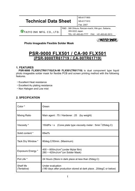
Technical Data Sheet PSR-9000 FLX501 / CA-90 FLX501
Technical Data Sheet PSR-9000 FLX501 / CA-90 FLX501
Technical Data Sheet PSR-9000 FLX501 / CA-90 FLX501

You also want an ePaper? Increase the reach of your titles
YUMPU automatically turns print PDFs into web optimized ePapers that Google loves.
<strong>Technical</strong> <strong>Data</strong> <strong>Sheet</strong><br />
TAIYO INK MFG. CO., LTD.<br />
MS-6171<strong>90</strong>0<br />
MS-6171910<br />
Feb. 2007<br />
R&D : 388 Ohkura, Ranzan-machi, Hiki-gun, Saitama,<br />
355-0222 Japan<br />
TEL +81-493-62-7777 FAX +81-493-62-3913<br />
Photo Imageable Flexible Solder Mask<br />
<strong>PSR</strong>-<strong><strong>90</strong>00</strong> <strong>FLX501</strong> / <strong>CA</strong>-<strong>90</strong> <strong>FLX501</strong><br />
(<strong>PSR</strong>-<strong><strong>90</strong>00</strong>TR61719 / <strong>CA</strong>-<strong>90</strong>TR61719)<br />
1. FEATURES<br />
<strong>PSR</strong>-<strong><strong>90</strong>00</strong> <strong>FLX501</strong>(TR61719)/<strong>CA</strong>-<strong>90</strong> <strong>FLX501</strong>(TR61719) is dual component type liquid<br />
photo imageable solder mask for flexible PCB and screen printing method with the following<br />
features.<br />
Excellent Heat resistance<br />
Excellent Au plating resistance<br />
Non Halogen and Low mist<br />
2. SPECIFI<strong>CA</strong>TION<br />
Color *<br />
Green<br />
Mixing Ratio<br />
Main agent : 75 / Hardener : 25 (by weight)<br />
Viscosity *<br />
150dPas (Cone plate type viscosity meter : 5min -1 /25deg.C)<br />
Solid content *<br />
69wt%<br />
Tack Dry Window *<br />
80deg.C/50min. (Maximum)<br />
Exposure Energy *<br />
Pot Life *<br />
Shelf life<br />
(Tentative)<br />
400 ~ 600mJ/cm 2 (under Mylar film)<br />
280 ~ 420mJ/cm 2 (on Solder Mask)<br />
24 Hours (Store in dark place at less than 25deg.C)<br />
Under evaluation<br />
(180 days after production stored at dark place , 20degC or below)<br />
1
* After mixing<br />
<strong>Technical</strong> <strong>Data</strong> <strong>Sheet</strong><br />
MS-6171<strong>90</strong>0<br />
MS-6171910<br />
<strong>PSR</strong>-<strong><strong>90</strong>00</strong>TR61719 / <strong>CA</strong>-<strong>90</strong>TR61719<br />
3. PROCESS CONDITIONS<br />
PROCESS CONDITION RANGE<br />
<br />
PWB FR-4, thickness 1.6mm -<br />
Pre-Treatment Acid treatment - Buff scrubbing -<br />
Printing<br />
# 100 mesh Tetron screen<br />
#100 ~ 125 mesh<br />
Tetron screen<br />
Hold Time 10 min. 10~20 min.<br />
Tack Free<br />
Exposure<br />
Double-sided printing<br />
1st printing : 80deg.C/20 min<br />
2nd printing: 80deg.C/25 min<br />
(Hot air convention oven)<br />
Single-sided printing<br />
80deg.C/30 min<br />
(Hot air convection oven)<br />
400mJ/cm 2 (under Mylar film)<br />
280mJ/cm 2 (on Solder Mask)<br />
80deg.C/15~20 min<br />
80deg.C/20~25 min<br />
80deg.C/30~40 min<br />
400mJ ~ 600mJ/cm 2<br />
280mJ ~ 420mJ/cm 2<br />
Hold Time 10 min. 10~20 min.<br />
Development<br />
Water Rinse<br />
Post cure<br />
Aqueous alkaline solution : 1wt%-Na 2 Co 3<br />
Temperature of developer : 30deg.C<br />
Spray pressure : 0.2MPa<br />
Dwelling time : <strong>90</strong> sec.<br />
Temperature : 25deg.C<br />
Spray pressure : 0.1MPa<br />
Dwelling time : 45 sec.<br />
150deg.C/60min. (Hot air convection oven)<br />
0.15 ~ 0.25MPa<br />
<strong>90</strong> ~ 120 sec.<br />
30deg.C or below<br />
0.1 ~ 0.15MPa<br />
45 ~ 60 sec.<br />
For legend ink process, post cure condition should be 150deg.C/30min before applying<br />
legend ink and set 140deg.C/20min X 2 times for final cure.<br />
150deg.C/60min for post cure is sufficient if no marking ink process.<br />
2
<strong>Technical</strong> <strong>Data</strong> <strong>Sheet</strong><br />
MS-6171<strong>90</strong>0<br />
MS-6171910<br />
<strong>PSR</strong>-<strong><strong>90</strong>00</strong>TR61719 / <strong>CA</strong>-<strong>90</strong>TR61719<br />
4. ATTENTION ON EACH PROCESS<br />
Operation environment should be clean room of 20~25deg.C and 50~60RH under<br />
yellow lamp(UV cut) avoiding fluorescent and sunlight.<br />
Open up the package when it becomes ambient temperature.<br />
Stir well before use<br />
Appropriate coating thickness on cupper circuits after thermal cure is 10um ~<br />
20um. Thinner coating thickness may cause lower resistance in solder heat,<br />
chemical and Ni/Au plating. Thick coating thickness may cause undercut and<br />
insufficient tackiness.<br />
Curing condition and window depend on oven type, batch size of work and curing<br />
condition of legend ink. Find the optimum condition of your own<br />
Exposure energy depends on material type of substrate or coating thickness.<br />
Find the optimum condition of your own based on resolution (undercut level),<br />
gross level, shoot-through, etc<br />
Control well the quality of developing agent in its density, temperature, spray<br />
pressure and dwelling time. Insufficient control may case deterioration in<br />
developing or undercut.<br />
Set optimum curing condition and window with consideration of curing<br />
condition for legend ink. Shortage or excess cure may cause degrade of<br />
coating properties.<br />
In case Ni/Au plating, set optimum curing condition and window with<br />
consideration of curing condition for legend ink. Over curing cause lower<br />
Ni/Au plating resistance.<br />
5. CHARACTERISTICS<br />
(1) DEVELOPMENT TOLERANCE WINDOW:<br />
Drying time<br />
(80deg.C/ min.)<br />
40 50 60 70<br />
Developability Clean Clean<br />
Slight<br />
Residue<br />
Residue<br />
(2) PHOTO SENSITIVITY:<br />
Item Thickness Energy Developing time Sensitivity<br />
Sensitivity<br />
Kodak No.2<br />
20 2um<br />
400mJ/cm 2<br />
(280mJ/cm 2 )<br />
500mJ/cm 2<br />
(350mJ/cm 2 )<br />
600mJ/cm 2<br />
(420mJ/cm 2 )<br />
<strong>90</strong> sec.<br />
6 step<br />
7 step<br />
8 step<br />
The exposure energy is measured on under artwork film (on solder mask) by using ORC<br />
HMW-680, 7Kw, metal halide lamp.<br />
3
<strong>Technical</strong> <strong>Data</strong> <strong>Sheet</strong><br />
MS-6171<strong>90</strong>0<br />
MS-6171910<br />
<strong>PSR</strong>-<strong><strong>90</strong>00</strong>TR61719 / <strong>CA</strong>-<strong>90</strong>TR61719<br />
6. PROPERTIES<br />
ITEM TEST METHOD RESULT<br />
Adhesion<br />
Pencil hardness<br />
TAIYO Internal Test Method<br />
Cross hatch/Tape peeling<br />
TAIYO Internal Test Method<br />
No scratch on copper surface<br />
100 / 100<br />
5H<br />
Solder heat resistance<br />
Solvent resistance<br />
Rosin flux 260deg.C/10sec, 1cycle<br />
Solder bath floating test<br />
PMA-AC, 20deg.C/20min. immersion<br />
Cross hatch/Tape peeling<br />
Pass<br />
Pass<br />
Acid resistance<br />
Alkaline resistance<br />
Insulation resistance<br />
Dielectric constant<br />
Dissipation factor<br />
Electroless Au plating<br />
10vol% HC1, H 2 SO 4<br />
20deg.C/20min. immersion,<br />
Cross hatch/Tape peeling<br />
10wt% NaOH, 20deg.C/20min.<br />
immersion, Cross hatch/Tape peeling<br />
IPC comb type B pattern<br />
25-65deg.C, <strong>90</strong>% RH<br />
DC100V for 7 days<br />
Measurement: DC500V / 1min.<br />
Value at room temperature<br />
25-65deg.C, <strong>90</strong>% RH<br />
DC100V for 7 days<br />
Measured at 1MHz / room<br />
temperature<br />
25-65deg.C, <strong>90</strong>% RH<br />
DC100V for 7 days<br />
Measured at 1MHz / room<br />
temperature<br />
Taiyo lab. Method<br />
Ni 3um / Au 0.03um<br />
Pass<br />
Pass<br />
Initial<br />
2.8 x 10 13 Ohm<br />
Conditioned<br />
6.6 x 10 12 Ohm<br />
Initial 4.3<br />
Conditioned 4.5<br />
Initial 0.030<br />
Conditioned 0.042<br />
Pass<br />
*All test data mentioned above in this technical data sheet are based on our laboratory test result and just for<br />
reference, not guarantee the same in your process.<br />
7. <strong>CA</strong>UTION<br />
All chemicals used in this product might have unknown toxicity. Please handle with your<br />
most care referring to the MSDS for use.<br />
Following substances restricted in EU RoHS Directive are not used in this product.<br />
Cadmium, Lead, Mercury, Hexavalent Chromium, Polybrominated Biphenyls(PBB) and<br />
Polybrominated Diphenyl Ether(PBDE).<br />
4