L7TA _Acer AL1716_ SERVICE GUIDE - Tehnari.ru
L7TA _Acer AL1716_ SERVICE GUIDE - Tehnari.ru
L7TA _Acer AL1716_ SERVICE GUIDE - Tehnari.ru

Create successful ePaper yourself
Turn your PDF publications into a flip-book with our unique Google optimized e-Paper software.
<strong>Acer</strong> <strong>AL1716</strong>(Dual)<br />
Service Guide<br />
Service guide files and updates are available on the CSD web: for more<br />
information,<br />
Please refer to http://csd.acer.com.tw/<br />
100% Recycled Paper<br />
- 1 -
Copyright<br />
Copyright © 2003 by <strong>Acer</strong> Incorporated. All rights reserved. No part of this publication may be reproduced,<br />
transmitted, transcribed, stored in a retrieval system, or translated into any language or computer language,<br />
in any form or by any means, electronic, mechanical, magnetic, optical, chemical, manual or otherwise,<br />
without the prior written permission of <strong>Acer</strong> Incorporated.<br />
Disclaimer<br />
The information in this guide is subject to change without notice. <strong>Acer</strong> Incorporated makes no<br />
representations or warranties, either expresses or implied, with respect to the contents hereof and<br />
specifically disclaims any warranties of merchantability or fitness for any particular purpose, Any <strong>Acer</strong><br />
Incorporated software described in this manual is sold or licensed “as is ”. Should the programs prove<br />
defective following their purchase, the buyer (and not <strong>Acer</strong> Incorporated, its distributor, of its dealer)<br />
assumes the entire cost of all necessary servicing, repair, and any incidental or consequential damages<br />
resulting from any defect in the software.<br />
<strong>Acer</strong> is a registered trademark of <strong>Acer</strong> Corporation.<br />
Intel is a registered trademark of Intel Corporation.<br />
Pentium and Pentium II/III are trademarks of Intel Corporation.<br />
Other brand and product names are trademarks and/or registered trademarks of their respective holders.<br />
- 2 -
Conventions<br />
The following conventions are used in this manual:<br />
Screen messages<br />
Denotes actual messages that appear on screen<br />
Note<br />
Warning<br />
Caution<br />
Important<br />
Gives bits and pieces of additional information related to<br />
the current topic.<br />
Alerts you to any damage that might result from doing or<br />
not doing specific actions.<br />
Gives precautionary measures to avoid possible hardware or<br />
software problems.<br />
Reminds you to do specific actions relevant to the<br />
accomplishment of procedures.<br />
- 3 -
Preface<br />
Before using this information and the product it supports, please read the following general information.<br />
1. This Service Guide provides you with all technical information relating to BASICCONFIGURATION<br />
decided for <strong>Acer</strong>’s “global” product offering. To better fit local market requirements and enhance product<br />
competitiveness, your regional office MAY have decided to extend the functionality of a machine (e.g.<br />
add-on card, modem, or extra memory capability). These LOCALIZED FEATURES will NOT be covered<br />
in this generic service guide. In such cases, please contact your regional offices or the responsible<br />
personnel/channel to provide you with further technical details.<br />
2. Please not WHEN ORDERING FRU PARTS, that you should check the most up-to-date information<br />
available on your regional web or channel. If, for whatever reason, a part number change is made, it will<br />
not be noted in the printed Service Guide, for ACER-AUTHORIZED <strong>SERVICE</strong> PROVIDERS, your <strong>Acer</strong><br />
office may have a DIFFERENT part number code to those given in the FRU list of this printed Service<br />
Guide. You MUST use the list provided by your regional <strong>Acer</strong> office to order FRU parts for repair and<br />
service of customer machines.<br />
- 4 -
WARNING: (FOR FCC CERTIFIED MODELS)<br />
NOTE: this equipment has been tested and found to comply with the limits for a Class B digital device,<br />
pursuant to Part 15 of the FCC Rules. These limits are designed to provide reasonable protection against<br />
harmful interference in a residential installation. This equipment generates, uses and can radiate radio<br />
frequency energy, and if not installed and used in accordance with the inst<strong>ru</strong>ctions, may cause harmful<br />
interference to radio communications. However, there is no guarantee that interference will not occur in a<br />
particular installation. If this equipment does cause harmful interference to radio or television reception,<br />
Which can be determined by turning the equipment off and on, the user is encouraged to try to correct the<br />
interference by one or more of the following measures:<br />
1. Reorient or relocate the receiving antenna.<br />
2. Increase the separation between the equipment and receiver.<br />
3. Connect the equipment into an outlet on a circuit different from that to which the receiver is connected.<br />
4. Consult the dealer or an experienced radio/TV technician for help.<br />
NOTICE:<br />
1. The changes or modifications not expressly approved by the party responsible for compliance could void<br />
the user’s authority to operate the equipment.<br />
2. Shielded interface cables and AC power cord, if any, must be used in order to comply with the emission<br />
limits.<br />
3. The manufacturer is not responsible for any radio or TV interference caused by unauthorized<br />
modification to this equipment. It is the responsibility of the user to correct such interference.<br />
As an ENERGY STAR ® Partner our company has determined that this product meets the ENERGY STAR ®<br />
guidelines for energy efficiency.<br />
WARNING:<br />
To prevent fire or chock hazard, do not expose the monitor to rain or moisture. Dangerously high<br />
voltages are present inside the monitor. Do not open the cabinet. Refer servicing to qualified<br />
personnel only.<br />
- 5 -
PRECAUTIONS<br />
• Do not use the monitor near water, e.g. near a bathtub, washbowl, kitchen sink, laundry tub,<br />
Swimming pool or in a wet basement.<br />
• Do not place the monitor on an unstable trolley, stand, or table. If the monitor falls, it can injure a<br />
person and cause serious damage to the appliance. Use only a trolley or stand recommended by the<br />
manufacture or sold with the monitor. If you mount the monitor on a wall or shelf, use a mounting kit<br />
approved by the manufacture and follow the kit inst<strong>ru</strong>ctions.<br />
• Slots and openings in the back and bottom of the cabinet area provided for ventilation. To ensure<br />
reliable operation of the monitor and to protect it from overheating, be sure these openings are not<br />
blocked or covered. Do not place the monitor on a bed, sofa, <strong>ru</strong>g or similar surface. Do not place the<br />
monitor near or over a radiator or heat register. Do not place the monitor in a bookcase or cabinet<br />
unless proper ventilation is provided.<br />
• The monitor should be operated only from the type of power source indicated on the label. If you are<br />
not sure of the type of power supplied to your home, consult your dealer or local power company.<br />
• The monitor is equipped with a three-pronged grounded plug, a plug with a third (grounding) pin. This<br />
plug will fit only into a grounded power outlet as a safety feature. If your outlet does not accommodate<br />
the three-wire plug, have an electrician install the correct outlet, or use an adapter to ground the<br />
appliance safely. Do not defeat the safety purpose of the grounded plug.<br />
• Unplug the unit during a lightning storm or when it will not be used for long periods of time. This will<br />
protect the monitor from damage due to power surges.<br />
• Do not overload power strips and extension cords. Overloading can result in fire or electric shock.<br />
• Never push any object into the slot on the monitor cabinet. It could short circuit parts causing a fire or<br />
electric shock. Never spill liquids on the monitor.<br />
• Do not attempt to service the monitor yourself; opening or removing covers can expose you to<br />
dangerous voltages and other hazards. Please refer all servicing to qualified service personnel.<br />
• To ensure satisfactory operation, use the monitor only with UL listed computers which have<br />
appropriate configured receptacles marked between 100-240V AC, Min. 3.5A.<br />
• The wall socket shall be installed near the equipment and shall be easily accessible.<br />
• For use only with the attached power adapter (output 12V DC) which have UL,CSA listed license<br />
- 6 -
SPECIAL NOTES ON LCD MONITORS<br />
The following symptoms are normal with LCD monitor and do not indicate a problem.<br />
NOTES<br />
• Due to the nature of the fluorescent light, the screen may flicker during initial use. Turn off the Power<br />
Switch and then turn it on again to make sure the flicker disappears.<br />
• You may find slightly uneven brightness in the screen depending on the desktop pattern you use.<br />
• The LCD screen has effective pixels of 99.99% or more. It may include blemishes of 0.01% or less such<br />
as a missing pixel or a pixel lit all of the time.<br />
• Due to the nature of the LCD screen, an afterimage of the previous screen may remain after switching<br />
the image, when the same image is displayed for hours. In this case, the screen is recovered slowly by<br />
changing the image or turning off the Power Switch for hours.<br />
- 7 -
Table of contents<br />
Chapter 1 MONITOR FEATURE<br />
………………………………………………………….9<br />
Chapter 2 OPERATING INSTRUTION … … … … … … … … … … … … … … … … … … … … .17<br />
Chapter 3 MACHINE ASSEMBLY ………………………………………………………. .22<br />
Chapter 4 TROUBLE SHOOTING<br />
………………………………………………………..35<br />
Chapter 5 CONNECTOR INFORMATION ………………………………………………37<br />
Chapter 6 FRU LIST<br />
………………………………………………………………………...39<br />
Chapter 7 SCHEMATIC DIAGRAM … … … … … … … … … … … … … … … … … … … … … ...40<br />
Chapter 8 POWER BOARD INFORMATION… …………………………………………….45<br />
- 8 -
Chapter 1<br />
Monitor Feature<br />
Driving system<br />
TFT Color LCD<br />
Size 17"<br />
Pixel pitch<br />
Viewable angle<br />
0.294 mm<br />
AU panel-12ms/8ms :70/60/70/70 degree(typ)<br />
LG panel-12ms:70/70/75/65 degree(typ)<br />
LG panel-8ms:70/70/70/70 degree(typ)<br />
Samsung-8ms:65/50/65/65 degree(typ)<br />
Samsung panel-13ms:75/60/75/75 degree(typ)<br />
CPT panel-12ms:67/63/70/70 degree(typ)<br />
CPT panel-8ms:65/65/70/70 degree(typ)<br />
QDI panel-8ms:65/60/70/70 degree(typ)<br />
HSDpanel-12ms:70/60/70/70 degree(typ)<br />
Brightness<br />
LG 8ms/12ms :250 cd/m 2 (typ.)<br />
AUO 8ms/12ms :300 cd/m 2 (typ.)<br />
Samsung–L21/L11 8ms/13ms: 300 cd/m 2 (typ.)<br />
CPT 8ms/12ms:300 cd/m 2 (typ.)<br />
HSD 12ms/ QDI 8ms:270 cd/m 2 (typ.)<br />
Contrast Ratio<br />
500:1 (AU M170EG01-V0/V2 ,8ms/12ms)<br />
600:1(LG LM170E01-TLA5/A6, 8ms)<br />
500:1(LG LM170E01-A6K1/A6, 12ms)<br />
700:1(Samsung LTM170EU-L21, 8ms)<br />
500:1(Samsung LTM170EU-L11, 13ms)<br />
500:1(CPT CLAA170EA07Q, 8ms)<br />
600:1(QDI QD170EL07 Rev11, 8ms)<br />
450:1(HSD HSD170ME13- A07,12ms)<br />
LCD Panel<br />
Response time<br />
8ms/12ms(AU) 8ms/12ms(LG) 8ms/13ms(Samsung)<br />
8ms/12ms(CPT) 8ms(QDI) HSD(12ms)<br />
Input Video R,G,B Analog,<br />
- 9 -
Separate Sync<br />
H-Frequency<br />
V-Frequency<br />
H/V TTL<br />
31-81KHZ<br />
56-75HZ<br />
Display Color<br />
Maximum Dot Clock ®<br />
Max Resolution<br />
Plug & Play<br />
16.2 million Colors<br />
135MHz<br />
1280x1024@75HZ<br />
VESA DDC2B<br />
ON Mode
Regulatory Compliance<br />
* Contrast/brightness<br />
* Focus<br />
* Clock<br />
* H.Position<br />
* W.Position<br />
* Language<br />
* OSD Color temperature<br />
* OSD Position & Timeout<br />
* Auto Config<br />
* Input<br />
* Information<br />
* Reset<br />
* Exit<br />
cUL, FCC, TUV, CE, ISO13406-2<br />
- 11 -
Timings<br />
The product has 26 memory modes in total. 16 modes are preset and 10 modes<br />
are user definable.<br />
MODE NO. 1 2 3 4<br />
RESOLUTION 720 x 400 640 x 480 640x480 640 x 480<br />
Dot clock(MHz) 28.321 25.175 30.240 31.500<br />
f h 31.469kHz 31.469kHz<br />
35.0kHz<br />
37.861kHz<br />
A ( us ) 31.78(900dots) 31.778 (800 dots) 28.571(864 dots) 26.413 (832 dots)<br />
B ( us ) 3.813(108dots) 3.813 (96 dots) 2.116 (64 dots) 1.270(40 dots)<br />
C ( us ) 1.907(54dots) 1.907 (48 dots) 3.175 (96 dots) 4.064(128 dots)<br />
D ( us ) 25.42(720dots) 25.422 (640 dots) 21.164 (640 dots) 20.317(640 dots)<br />
E ( us ) 0.636(18dots) 0.636 (16 dots) 2.116 (64 dots) 0.762(24 dots)<br />
f v 70Hz(70.087) 60Hz (59.940) 66.7 HZ (66.667) 72.809Hz<br />
O (ms ) 14.27(449 lines) 16.683 (525<br />
15.000 (525 lines ) 13.735(520 lines)<br />
lines )<br />
P ( ms ) 0.064(2 lines) 0.064 (2 lines ) 0.086 (3 lines ) 0.079(3 lines)<br />
Q (ms ) 1.112(35 lines) 1.049 (33 lines ) 1.114 (39 lines ) 0.739(28 lines)<br />
R ( ms ) 12.71(400 lines) 15.253 (480<br />
13.714 (480 lines ) 12.678(480 lines)<br />
lines )<br />
S ( ms ) 0.384(12 lines) 0.317 ( 10 lines) 0.086 (3 lines ) 0.237(9 lines)<br />
SYNC. H/V -/+ - / - +/+ -/-<br />
POLARITY Or -/-<br />
SEP . SYNC Y Y Y Y<br />
MODE NO. 5 6 7 8<br />
RESOLUTION 640 x 480 800 x 600 800 x 600 800 x 600<br />
Dot clock(MHz) 31.500 36.000 40.000 49.500<br />
f h 37.500kHz 35.16kHz 37.879kHz 46.875kHz<br />
A ( us ) 26.667(840 dots) 28.44(1024 dots) 26.40 (1056 dots) 21.333 (1056dots)<br />
- 12 -
B ( us ) 2.032 (64 dots) 2.00(72 dots) 3.200 (128 dots) 1.616 (80 dots)<br />
C ( us ) 3.810 (120 dots) 3.56(128 dots) 2.200 ( 88 dots) 3.232 (160 dots)<br />
D ( us ) 20.317 (640 dots) 22.22(800 dots) 20.00 ( 800 dots) 16.162 (800 dots)<br />
E ( us ) 0.508 (6 dots) 0.67(24 dots) 1.000 (40 dots) 0.323 (16 dots)<br />
f v 75Hz (75) 56.25 60Hz (60.316) 75Hz (75.000)<br />
O (ms ) 13.333 (500<br />
17.78(625 lines) 16.58 (628 lines) 13.333 (625lines)<br />
lines)<br />
P ( ms ) 0.080 (3 lines) 0.06(2 lines) 0.106 (4 lines) 0.064 (3 lines)<br />
Q (ms ) 0.427 (16 lines) 0.63(22 lines) 0.607 (23 lines) 0.448 (21 lines)<br />
R ( ms ) 12.80 (480 lines) 17.07(600 lines) 15.84 (600 lines) 12.80 (600lines)<br />
S ( ms ) 0.027 ( 1 line ) 0.03( 1 line) 0.026 (1 line ) 0.021 (1 line )<br />
SYNC. H/V - / - +/+ + / + + / +<br />
POLARITY<br />
SEP . SYNC Y Y Y Y<br />
MODE NO. 9 10 11 12<br />
RESOLUTION 800 x 600 832 x 624 1024 x 768 1024 x 768<br />
Dot clock(MHz) 50.000 57.283 65.000 75.000<br />
f h 48.077kHz 49.72kHz 48.363kHz 56.48kHz<br />
A ( us ) 20.80 (1040dots) 20.11(1152 dots) 20.677(1344 dots) 17.71(1328 dots)<br />
B ( us ) 2.400 ( 120 dots) 1.12(64 dots) 2.092(136 dots) 1.81(136 dots)<br />
C ( us )<br />
1.280 (64 dots) 3.91(224 dots) 2.462(160 dots) 1.92(144 dots)<br />
D ( us ) 16.00 (800 dots) 14.52( 832 dots ) 15.754(1024 dots) 13.65(1024 dots)<br />
E ( us ) 1.120 (56 dots) 0.56(32 dots ) 0.369(24 dots) 0.32(24 dots)<br />
f v 72Hz (72.188) 74.55Hz 60.004Hz 70.07Hz<br />
O (ms ) 13.85 (666 lines) 13.41(667 lines) 16.666(806 lines) 14.27(806 lines)<br />
P ( ms ) 0.125 (6 lines) 0.06(3 lines) 0.124(6 lines) 0.11(6 lines)<br />
Q (ms ) 0.478 (23 lines) 0.78(39 lines) 0.600(29 lines) 0.51(29 lines)<br />
R ( ms ) 12.48 (600 lines) 12.55 (624 lines) 15.880(768 lines) 13.60(768 lines)<br />
S ( ms ) 0.770 ( 37<br />
0.02(1 line) 0.062(3 lines) 0.05(3 lines)<br />
line )<br />
SYNC. H/V + / + +/+ -/- -/-<br />
- 13 -
POLARITY<br />
SEP . SYNC Y Y Y Y<br />
MODE NO. 13 14 15 16<br />
RESOLUTION 1024 x 768 1280 x 1024 1280 x 1024 1152 x 864<br />
Dot clock(MHz) 78.750 108.000 135 108.00<br />
f h 60.02kHz 63.981kHz 79.976KHz 67.5 KHz<br />
A ( us ) 16.66(1312 dots) 15.630 (1688<br />
12.504 (1688 dots) 14.815(1600 dots)<br />
dots)<br />
B ( us ) 1.22 (96 dots) 1.037 (112 dots) 1.067 (144 dots) 1.185(128 dots)<br />
C ( us ) 2.23 (176 dots) 2.296 (248 dots) 1.837 (248 dots) 2.370(256 dots)<br />
D ( us ) 13.00 (1024 dots) 11.852 (1280<br />
9.481 (1280dots) 10.667(1152 dots)<br />
dots)<br />
E ( us ) 0.20 (16 dots) 0.444 (48 dots) 0.119 (16 dots) 0.593(64 dots)<br />
f v 75.03Hz 60.020Hz 75.025 Hz 75.06 Hz<br />
O (ms ) 13.33 (800 lines) 16.661 (1066<br />
13.329 (1066 lines) 13.333(900 lines)<br />
lines)<br />
P ( ms ) 0.05 (3 lines) 0.047 ( 3 lines) 0.038 (3 lines) 0.044(3 lines)<br />
Q (ms ) 0.47 (28 lines) 0.594 ( 38 lines) 0.475 (38 lines) 0.474(32 lines)<br />
R ( ms ) 12.80 (768 lines) 16.005 (1024<br />
12.804(1024 lines) 12.800(864 lines)<br />
lines)<br />
S ( ms ) 0.02 (1 lines) 0.016 (1 line ) 0.013 (1 lines) 0.015(1 lines)<br />
SYNC. H/V -/- +/+ +/+ +/+<br />
POLARITY<br />
SEP . SYNC Y Y Y Y<br />
A<br />
: H-Total<br />
O<br />
: V-Total<br />
B : H- Sync width P : V- Sync width<br />
C : H- Back porch Q :.V- Back porch<br />
D : H- Video width R : V- Video width<br />
E : H- Front porch S :.V- Front porch<br />
- 14 -
]<br />
Monitor Block Diagram<br />
- 15 -
PCB CONDUCTOR VIEW<br />
Main Board<br />
- 16 -
Chapter 2<br />
OPERATING INSTRUCTIONS<br />
Front Panel Definition<br />
This Section defines the front panel User Interface for Led Indictor and Key function.<br />
Key Definition:<br />
There are five keys defined in this system and described bellows.<br />
External Controls<br />
Power on/off<br />
?1 POWER<br />
Blue: power on<br />
?2<br />
OSD<br />
Function<br />
Orange: in sleep mode<br />
Press to view OSD.<br />
Press again to exit a selection in OSD.<br />
?3 UP/ PLUS<br />
If OSD is active, press to select or adjust OSD options. If OSD<br />
is inactive, press once, then press the buttons marked or<br />
to adjust the volume.<br />
?4<br />
DOWN /<br />
MINUS<br />
If OSD is active, press to select or adjust OSD options. If OSD<br />
is inactive, press once, then press the buttons marked or<br />
to adjust the volume.<br />
?5 AUTO<br />
If OSD is active, press to enter a selection in OSD. If OSD is<br />
inactive, press and the monitor will automatically optimize the<br />
position, focus and clock of your display.<br />
- 17 -
OSD Menu<br />
Picture<br />
Brightness:<br />
This adjusts the brightness of the picture on the screen.<br />
Contrast:<br />
This adjusts dark and light shades of color relative to each other to<br />
achieve a comfortable contrast.<br />
Color temp. :<br />
There are three ways of adjusting color:<br />
Warm (Reddish white)<br />
Cool (Bluish white)<br />
User : You can adjust the colors red, green and blue to the intensity<br />
you desire.<br />
Focus:<br />
This removes any horizontal distortion and makes the picture clear<br />
and sharp.<br />
Clock:<br />
If there are any vertical stripes seen on the background of the screen<br />
this renders them less noticeable by minimizing their size. It also<br />
changes the size of the horizontal screen.<br />
H-Position:<br />
This adjusts the horizontal screen position.<br />
V-Position:<br />
This adjusts the vertical screen position.<br />
- 18 -
Option<br />
Auto Config. :<br />
System <strong>ru</strong>ns auto-configuration.<br />
Reset:<br />
Recall to default settings.<br />
Information:<br />
This shows brief information on the screen.<br />
Setting<br />
Language:<br />
Select the OSD menu language from<br />
English, French, German, Italian, Spanish, Simplified Chinese,<br />
Traditional Chinese, Japanese and Russian.<br />
OSD H. Position<br />
OSD V. Position<br />
OSD Time-out<br />
This changes the position of the OSD window on the screen and staying<br />
time.<br />
- 19 -
LED Definition<br />
The system equips one dual color (blue/amber) led to indict system status and defined as bellows :<br />
LED Color<br />
Blue<br />
Amber<br />
System Status<br />
System in normal operation mode<br />
System in power-saving mode<br />
Dark<br />
System in power-off mode<br />
LOGO :<br />
When the monitor is power on, the LOGO will be showed in the center, and disappear slowly.<br />
HOW TO OPTIMIZE THE DOS-MODE<br />
Plug and play<br />
Plug & play DDC2B feature<br />
This monitor is equipped with VESA DDC2B capabilities according to the VESA DDC STANDARD. It<br />
allows the monitor to inform the host system of its identity and, depending on the level of DDC used,<br />
communicate additional information about its display capabilities. The communication channel is defined in<br />
two levels, DDC2B.<br />
The DDC2B is a bi-directional data channel based on the I 2 C protocol. The host can request EDID<br />
information over the DDC2B channel.<br />
- 20 -
THIS MONITOR WILL APPEAR TO BE NON-FUNCTIONAL IF THERE IS NO VIDEO INPUT<br />
SIGNAL. IN ORDER FOR THIS MONITOR TO OPERATE PROPERLY, THERE MUST BE A<br />
VIDEO INPUT SIGNAL.<br />
This monitor meets the Green monitor standards as set by the Video Electronics Standards<br />
Association(VESA) and/or the United States Environmental Protection Agency (EPA) and The Swedish<br />
Confederation Employees (NUTEK). This feature is designed to conserve electrical energy by reducing<br />
power consumption when there is no video-input signal present. When there is no video input signal this<br />
monitor, following a time-out period, will automatically switch to an OFF mode. This reduces the monitor’s<br />
internal power supply consumption. After the video input signal is restored, full power is restored and the<br />
display is automatically redrawn. The appearance is similar to a “Screen Saver” feature except the display is<br />
completely off. The display is restored by pressing a key on the keyboard, or clicking the mouse.<br />
USING THE RIGHT POWER CORD<br />
The accessory power cord for the Northern American region is the wallet plug with NEMA 5-15 style and is<br />
UL listed and CSA labeled. The voltage rating for the power cord shall be 125 volt AC.<br />
Supplied with units intended for connection to power outlet of personal computer: Please use a cord set<br />
consisting of a minimum No. 18 AWG, type SJT or SVT three conductors flexible cord. One end terminates<br />
with a grounding type attachment plug, rated 10A, 250V,CEE-22 male configuration. The other end<br />
terminates with a molded-on type connector body, rated 10A, 250V, having standard CEE-22 female<br />
configuration.<br />
Please note that power supply card needs to use VDE 0602, 0625, 0821 approval power cord in European<br />
counties.<br />
- 21 -
Chapter 3<br />
Machine assembly<br />
This chapter contains step-by-step procedures on how to assemble the monitor for maintenance and<br />
trouble shooting<br />
NOTE : 1. The screws for the different components vary in size. During the disassembly process, group the<br />
screws with the corresponding to avoid mismatch when putting back the components.<br />
2. Note : The monitor surface is susceptible to scratching! Therefore, lay the monitor on a soft<br />
surface when mounting or removing the base.<br />
3. Wear gloves.<br />
Front View : ( unit : mm )<br />
- 22 -
Real View :<br />
Top View :<br />
- 23 -
Side View : ( unit : mm )<br />
Assembly process<br />
Picture<br />
Description<br />
1. [GET PCB SHIELD AND PUT IT IN THE<br />
MIDDLE OF CONVEYER]<br />
2. [GET M/B AND LCD CABLE,THEN<br />
INSERT LCD CABLE IN M/B<br />
CONNECTOR]<br />
3. [GET BUTTON CABLE,THEN INSERT IT<br />
INTO M/B CONNECTOR]<br />
- 24 -
1<br />
2<br />
1. [GET POWER/B]<br />
2. [INSERT JUMPER IN THE APPOINTED<br />
PLACE OF JP10 ON POWER/B]<br />
3. [USE AGGLUTINANT TO STICK THE<br />
JUMPER AND POWER/B]<br />
4. [MARK A DOT IN THE PANE MARK OF<br />
POWER/B AS PICTURE SHOWS]<br />
5<br />
5. [ASSEMBLE M/B AND P/B ON PCB<br />
SHIELDING]<br />
1. [USE 3*PCS SCREW(M3*6-B) TO FIX<br />
POWER/B]<br />
2. [USE 3*PCS SCREW(M3*6-B)TO FIX M/B]<br />
- 25 -
1. [USE 1*PCS SCREW(M3.5*8-B) TO FIX<br />
POWER/B AT THE APPOINTED PLACE]<br />
2.[GET POWER/B MYLAR AND STICK ON<br />
THE APPOINTED PLACE]<br />
3. [GET BUTTON CABLE THROUGH THE<br />
APPOINTED HOLE]<br />
1. [MOVE PCB SHIELD TO THE FRONT OF<br />
CONVEYER]<br />
2. [GET PANEL AND PUT IT ON THE<br />
CONVEYER, THEN TEAR OFF THE<br />
INCOMING TAPE]<br />
- 26 -
1.[GET PANEL PROTECTIVE FILM AWAY<br />
AND INSPECT IF PANEL IS DIRTY OR<br />
SCRATCHED]<br />
2.[ USE ADHESIVE TAPE TO STICK THE<br />
PROTECTIVE FILM TO PANEL]<br />
3.[TURN LCD TO BACKSIDE ANDTEAR OFF<br />
INCOMING TYPE]<br />
1. [STICK RUBBER 2PCS ON BKT-L]<br />
2.[STICK RUBBER 2PCS ON BKT-R]<br />
1. [GET LEFT BKT , LOCK 2*PCS SCREW<br />
TO FASTEN IT ON THE PANEL]<br />
- 27 -
1.[STICK 1*PCS LCD MYLAR TO THE BACK<br />
OF PANEL]<br />
2.[GET RIGHT BKT , LOCK 2*PCS SCREW<br />
TO FASTEN IT ON THE PANEL]<br />
3. [TURN LCD AND TEAR OFF<br />
PROTECTIVE FILM]<br />
1. [GET BEZEL AND CHECK ITS<br />
APPEARANCE]<br />
2. [ASSEMBLE BEZEL ON PANEL]<br />
3. [STICK TYPE ON PROTECTIVE<br />
FILM]<br />
- 28 -
4. [TURN LCD]<br />
5. [FETCH TRAVEL CARD, TEAR OFF<br />
1*PCS APPOINTED S/N FROM TRAVEL<br />
CARD AND PASTE IT ON THE RIGHT<br />
BKT]<br />
1. [SCAN S/N AND POWER CODE]<br />
2. [FASTEN BKT AND BEZEL IN THE RIGHT<br />
SIDE WITH SCREW 3*PCS ]<br />
1. [FASTEN BKT AND BEZEL IN THE RIGHT<br />
SIDE WITH SCREW 3*PCS ]<br />
- 29 -
1. [GET SHIELD ON THE BKT R/L AND<br />
[INSERT LCD CABLE INTO PANEL<br />
CONNECTOR]<br />
2. [STICK 1*PCS YELLOW TAPE TO<br />
FASTEN LCD CABLE]<br />
3. [TRIM WIRES AND ASSEMBLE<br />
SHIELDING IN RIGHT POSITION]<br />
1. [LOCK 4*PCS SCREW(M3*3-I) TO<br />
FASTEN PCB SHIELD]<br />
2. [FETCH BUTTON AND PUT IT IN THE<br />
MIDDLE OF CONVEYER]<br />
1. [FASTEN 2*PCS IO-NUT TO VGA IN THE<br />
M/B]<br />
- 30 -
1. [STICK 1*PCS AL FOIL ON THE<br />
APPOINTED PLACE AS PICTURE<br />
SHOWS]<br />
2. [INSERT SUPERIOR CCFT CABLE IN<br />
POWER/B]<br />
1. [FETCH BUTTON&ITS CABLE,THEN<br />
ASSEMBLE THEM]<br />
2. [ASSEMBLE BUTTON/B AND BEZEL]<br />
3. [LOCK 3*PCS SCREW(F3*5-I) TO<br />
FASTEN BUTTON/B ON THE BEZEL]<br />
1. [PASTE YELLOW TAPE TO FASTEN<br />
BUTTON/B CABLE]<br />
2. [INSERT LOWER CCFT CABLE IN<br />
POWER/B]<br />
- 31 -
1. [STICK 1*PCS AL FOIL CONNECT<br />
PANEL AND SHIELDING]<br />
2. [STICK 1*PCS AL FOIL TO COVER<br />
UPPER CCFT CABLE]<br />
3. [STICK 1*PCS AL FOIL TO COVER<br />
LOWER CCFT CABLE]<br />
1. [GET LCD COVER AND INSPECT ITS<br />
APPEARANCE]<br />
2. [ASSEMBLE LCD COVER TO BEZEL]<br />
- 32 -
1. [FETCH TRAVEL CARD, TEAR OFF 1*PCS<br />
APPOINTED S/N FROM TRAVEL CARD<br />
AND PASTE IT ON THE COVER]<br />
2. [LOCK 2*PCS SCREW (F3*8-B) TO<br />
FASTEN BEZEL AND LCD COVER]<br />
3. [GET STAND NECK AND INSPECT IF IT IS<br />
DIRTY AND SCRATCHED, THEN PUT IT<br />
IN THE CONVEYER]<br />
1. [AT FIRST CHECK IF 2*PCS SCREW IN<br />
THE COVER IS LOST]<br />
2. [LOCK 4*PCS SCREW (M4*10-B) TO<br />
FASTEN STAND NECK]<br />
1. [GET BASE FIXTURE AND<br />
ASSEMBLE IT TO STAND NECK]<br />
2. [GET HINGE CAP AND<br />
ASSEMBLE IT ONTO HINGE ]<br />
3. [STAND LCD MONITOR UP]<br />
- 33 -
1. [INSERT VGA CABLE IN VGA<br />
CONNECTOR]<br />
2. [INSERT DVI CABLE IN VGA<br />
CONNECTOR]<br />
- 34 -
Chapter 4<br />
TROUBLE SHOOTING<br />
This chapter provides trouble shooting information for<strong>AL1716</strong><br />
1. No Power<br />
No Power<br />
Check Power Board<br />
Output<br />
CN1 Pin 5,Pin6 =5V<br />
NO<br />
Change Adaptor Power Board<br />
OK<br />
Check Scalar Module<br />
Output<br />
EC1 =5V?<br />
R175 = 3.3V ?<br />
NO<br />
Change Scalar Module Board<br />
OK<br />
Check Power Button<br />
From Scalar/B(CN6)<br />
to Button/B(CN1)<br />
NO<br />
Check Cable<br />
Open ?<br />
Yes<br />
Change Cable<br />
NO<br />
Change Switch or Button Board<br />
- 35 -
2. No Characters, Missing one color<br />
No Characters<br />
Missing one color<br />
Check CN2,CN3<br />
VGA,DVI Cabel?<br />
No<br />
F/W adjust<br />
OK<br />
No<br />
Check U7<br />
Re-Adjust<br />
Output?<br />
<br />
OK<br />
Check CN5<br />
LVDS Cable<br />
No<br />
Change LVDS<br />
Cable<br />
OK<br />
Change Panel<br />
- 36 -
Chapter 5<br />
Connector Information<br />
Phonejack stereo<br />
PIN1. AC power cord<br />
PIN2. Audio cable<br />
PIN3. Audio<br />
: CEE22 typed connector<br />
: Line-in receptacle<br />
The PIN assignment of the 15 pin mini D-SUB connector / cable is as follows:<br />
PI MNEM SIGNAL<br />
1 RV Red Video<br />
2 GV Green Video<br />
3 BV Blue Video<br />
4 NC None<br />
5 GND Ground(DDC return)<br />
6 RG Red GND<br />
7 GG Green GND<br />
8 BG Blue GND<br />
9 +5V + 5V (for DDC)<br />
10 SG Sync GND<br />
11 NC None<br />
12 SDA DDC Data<br />
13 HS Horizontal Sync<br />
14 VS Vertical Sync<br />
15 SCL DDC Clock<br />
- 37 -
The PIN assignment of the 24 pin DVI D connector / cable is as follows:<br />
PIN Signal<br />
1 TMDS data2-<br />
2 TMDS data2+<br />
3 TMDS data2 shield<br />
4 NC<br />
5 NC<br />
6 DDC clock<br />
7 DDC data<br />
8 Not connected<br />
9 TMDS data1-<br />
10 TMDS data1+<br />
11 TMDS data1 shield<br />
12 NC<br />
13 NC<br />
14 +5V<br />
15 Ground (return for +5 V and H/V<br />
sync)<br />
16 Hot plug detect<br />
17 TMDS data0-<br />
18 TMDS data0+<br />
19 TMDS data0 shield<br />
20 NC<br />
21 NC<br />
22 TMDS clock shield<br />
23 TMDS clock+<br />
24 TMDS clock-<br />
- 38 -
FRU (Field Replaceable Unit) list<br />
Chapter 6<br />
This chapter gives you the FRU (Field Replaceable Unit) listing in global configurations of AL1511.<br />
Refer to this chapter whenever ordering for parts to repair or for RMA (Return Merchandise<br />
Authorization).<br />
NOTE : Please note WHEN ORDERING FRU PARTS, that you should check the most up-to-date<br />
information available on your regional web or channel(http://aicsl.acer.com.tw/spl/). For whatever<br />
reasons a part number change is made, it will not be noted in the printed Service Guide. For<br />
ACER-AUTHORIZED CERVICE PROVIDERS, your <strong>Acer</strong> office may have a DIFFERENT part<br />
number code to those given in the FRU list of this printed Service Guide. You MUST use the local<br />
FRU list provided by your regional <strong>Acer</strong> office to order FRU parts repair and service of customer<br />
machines.<br />
NOTE: To scrap or to return the defective parts, you should follow the local government ordinance or<br />
regulations on how best to dispose it, or follow the <strong>ru</strong>les set by your regional <strong>Acer</strong> office on how to<br />
return it.<br />
- 39 -
5<br />
4<br />
3<br />
2<br />
1<br />
D<br />
CN1 CONN 4x2-R<br />
12V<br />
1 2<br />
3 4<br />
5 6<br />
7 8<br />
L3<br />
C102<br />
1U/6<br />
FUSE1<br />
0<br />
1 2<br />
10K/6 1<br />
3DVCC<br />
Q3<br />
MMST3906<br />
C11<br />
C4<br />
0.1u/6<br />
0.1U/6<br />
R8<br />
0/6<br />
3DVCC<br />
R10<br />
10K/6<br />
R14<br />
10K/6/NC<br />
3DVCC<br />
R1,L1<br />
C5<br />
0.1u/6<br />
R13 1K/6<br />
VCC12<br />
C6<br />
220u/16V<br />
VRMT<br />
L32<br />
FEB_0805<br />
TO252 package<br />
+<br />
EC2<br />
10uF/16V<br />
U1 AIC1117CY<br />
3<br />
VIN VOUT<br />
2<br />
VO<br />
4<br />
GND<br />
1<br />
U2 AIC1117CY<br />
2<br />
VIN VOUT<br />
3<br />
GND<br />
5DVCC<br />
EC1<br />
330u/16V<br />
R6<br />
330/6 1%<br />
+<br />
EC3<br />
10uF/16V<br />
C3<br />
5DVCC<br />
3DVCC_1 3DVCC<br />
R175 0/6<br />
0.1u/6<br />
U1 與 U' 共 同 layout<br />
3DVCC<br />
3AVCC1<br />
3PVCC<br />
3AVCC2<br />
3 C<br />
2 1 E<br />
RTD 3DVCC<br />
ADC_ 3AVCC<br />
RTD 3PVCC<br />
LVDS_3AVCC<br />
D<br />
C<br />
C<br />
Modify<br />
3DVCC<br />
VBRI<br />
VCPU<br />
2 R176 0/6<br />
R16<br />
1K/6<br />
R18<br />
4.7K/6<br />
3<br />
1<br />
Q4<br />
SN7002E<br />
2<br />
DEL R173,R174; ADD D1<br />
2.5DVCC_1<br />
2.5DVCC<br />
2.5DVCC<br />
RTD 2.5DVCC<br />
B<br />
DSUB_5V<br />
B<br />
3DVCC<br />
1<br />
D1<br />
1N4148<br />
SOT223 package<br />
U3 AIC1117CY<br />
3<br />
VIN VOUT<br />
2<br />
VO<br />
4<br />
+<br />
R144<br />
4.7K/6<br />
For layout<br />
A<br />
3<br />
3 4<br />
4<br />
2<br />
2 5<br />
5<br />
1<br />
1<br />
A<br />
5<br />
4<br />
3<br />
9<br />
8<br />
7<br />
6<br />
9<br />
8<br />
7<br />
6<br />
GND<br />
1<br />
R15<br />
200/6 1%<br />
+<br />
EC6<br />
10uF/16V<br />
C12<br />
0.1u/6<br />
CX201209805/8<br />
L28<br />
C100<br />
0.1u/6<br />
3<br />
3 4<br />
4<br />
2<br />
2 5<br />
5<br />
1<br />
1<br />
3<br />
3 4<br />
4<br />
2<br />
2 5<br />
5<br />
1<br />
1<br />
9<br />
8<br />
7<br />
6<br />
9<br />
8<br />
7<br />
6<br />
9<br />
8<br />
7<br />
6<br />
9<br />
8<br />
7<br />
6<br />
1<br />
1<br />
C1<br />
0.1u/6<br />
R3<br />
200/6 1%<br />
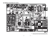
Chapter 7<br />
C13<br />
1U/8<br />
NC/CX201209805/8<br />
L27<br />
EC5<br />
10uF/16V<br />
R17<br />
200/6 1%<br />
D30<br />
1N4148<br />
D31<br />
1N4148<br />
Q18<br />
MMBT3906<br />
1 3<br />
C101<br />
NC/6<br />
R143<br />
4.7K/6<br />
2<br />
Q19<br />
MMBT3906<br />
1<br />
1<br />
1 3<br />
3<br />
3 4<br />
4<br />
2<br />
2 5<br />
5<br />
1<br />
1<br />
9<br />
8<br />
7<br />
6<br />
9<br />
8<br />
7<br />
6<br />
2<br />
2<br />
Title<br />
Power<br />
Size Document Number Rev<br />
DISPLAY<br />
B2B<br />
Date: Friday, August 12, 2005<br />
Sheet 3 of 7<br />
1<br />
- 40 -
5<br />
4<br />
3<br />
2<br />
1<br />
D<br />
CN2<br />
11<br />
DDC_SDA 12<br />
IN-H 13<br />
IN-V 14<br />
DDC_SCL 15<br />
VGA/NC<br />
16<br />
17<br />
1<br />
6<br />
2<br />
7<br />
3<br />
8<br />
4<br />
9<br />
5<br />
10<br />
PAGE1 VGA<br />
INPUT<br />
DDC_SDA<br />
RED+IN<br />
RED-IN<br />
GREEN+IN<br />
GREEN-IN<br />
BLUE+IN<br />
BLUE-IN<br />
DSUB_5V<br />
DSUB_5V<br />
PIN 10 VGA_CON<br />
DDC_SCL<br />
L8<br />
RED+IN<br />
RED-IN<br />
L9<br />
GREEN+IN<br />
GREEN-IN<br />
FCB1608C-190T03/6<br />
R23 100/6<br />
R24<br />
C17<br />
10pF<br />
75/6/F R25 100/6<br />
FCB1608C-190T03/6<br />
R26 100/6<br />
R27<br />
C20<br />
10pF<br />
75/6/F<br />
R28 100/6<br />
R29 100/6<br />
C16<br />
C18<br />
C19<br />
C21<br />
C22<br />
0.047u/6<br />
0.047u/6<br />
0.047u/6<br />
0.047u/6<br />
0.047u/6<br />
RED+<br />
RED-<br />
GREEN+<br />
GREEN-<br />
SOGIN<br />
D<br />
R30<br />
1M/6<br />
C<br />
GND<br />
IN-H<br />
DDC_SCL<br />
RED-IN<br />
GREEN-IN<br />
BLUE-IN<br />
ADC_VCC<br />
1<br />
3<br />
5<br />
7<br />
9<br />
11<br />
13<br />
CN3<br />
+<br />
+<br />
+<br />
+<br />
+<br />
+<br />
+<br />
+<br />
+<br />
+<br />
+<br />
+<br />
+<br />
+<br />
2<br />
4<br />
6<br />
8<br />
10<br />
12<br />
14<br />
NC/VGA INPUT<br />
RED+IN<br />
GREEN+IN<br />
BLUE+IN<br />
GND<br />
IN-V<br />
DDC_SDA<br />
DSUB_5V<br />
BLUE+IN<br />
BLUE-IN<br />
L10<br />
FCB1608C-190T03<br />
R32<br />
75/6/F<br />
IN-H<br />
R31 100/6 C23<br />
C24<br />
10pF<br />
R33 100/6 C25<br />
L31 FCM1608C-300T06/6<br />
R34 100/6 VGAHS<br />
R35<br />
C26<br />
2K/6<br />
10P/6/NC<br />
0.047u/6<br />
0.047u/6<br />
1 2<br />
D34<br />
Z3.3V<br />
BLUE+<br />
BLUE-<br />
AHS<br />
C<br />
D7<br />
DAN217K<br />
RED+IN<br />
3<br />
2<br />
D8<br />
DAN217K<br />
GREEN+IN 3<br />
2<br />
D9<br />
DAN217K<br />
BLUE+IN<br />
3<br />
2<br />
IN-V<br />
R37<br />
2K/6<br />
R36 100/6 VGAVS<br />
C28<br />
22P/6/NC<br />
1 2<br />
D35<br />
Z3.3V<br />
AVS<br />
1<br />
1<br />
1<br />
IN-H<br />
IN-V<br />
DDC_SDA<br />
DDC_SCL<br />
Bus_Power<br />
3DVCC<br />
3DVCC<br />
1 2<br />
D10<br />
Z5.6<br />
1 2<br />
D11<br />
Z5.6<br />
1 2<br />
D12<br />
Z5.6<br />
1 2<br />
D13<br />
Z5.6<br />
D17<br />
BAT54C-GS08<br />
C29<br />
0.1U/6<br />
B<br />
A<br />
25<br />
CN4<br />
TXC+<br />
TXC-<br />
RX2-<br />
RX2+<br />
GND<br />
RX4-<br />
RX4+<br />
SCL<br />
SDA<br />
VS<br />
RX1-<br />
RX1+<br />
GND<br />
RX3-<br />
RX3+<br />
5V<br />
GND<br />
HP<br />
RX0-<br />
RX0+<br />
GND<br />
RX5-<br />
RX5+<br />
GND<br />
RXC+<br />
RXC-<br />
1<br />
2<br />
3<br />
4<br />
5<br />
6<br />
7<br />
8<br />
9<br />
10<br />
11<br />
12<br />
13<br />
14<br />
15<br />
16<br />
17<br />
18<br />
19<br />
20<br />
21<br />
22<br />
23<br />
24<br />
DDC2_SCL<br />
DDC2_SDA<br />
R48 10K/6<br />
Bus_Power<br />
1 2<br />
1 2<br />
D18<br />
Z5.6<br />
D20<br />
Z5.6<br />
1 2<br />
1 2<br />
D19<br />
Z5.6<br />
D21<br />
Z5.6<br />
R155 0<br />
R156 0<br />
R157 0<br />
R158 0<br />
R159 0<br />
R160 0<br />
R161 0<br />
R162 0<br />
TX2-<br />
TX2+<br />
TX1-<br />
TX1+<br />
TX0-<br />
TX0+<br />
U5<br />
1<br />
NC VCC<br />
8<br />
2<br />
NC VCLK<br />
7<br />
3<br />
NC SCK<br />
6<br />
4<br />
VSS SDA<br />
5<br />
M24LC02<br />
1 2<br />
R44<br />
2K/6<br />
1 2<br />
D22<br />
Z5.6/NC<br />
R45<br />
2K/6<br />
D23<br />
Z5.6/NC<br />
R46 100/6<br />
R47 100/6<br />
DDC2_SCL<br />
DDC2_SDA<br />
B<br />
A<br />
26<br />
DVI-D/NC<br />
5<br />
C31<br />
1U/6NC<br />
1 2<br />
D24<br />
Z5.6<br />
C30<br />
0.1U/6<br />
1 2<br />
D25<br />
Z5.6<br />
4<br />
1 2<br />
D26<br />
Z5.6<br />
1 2<br />
D27<br />
Z5.6<br />
1 2<br />
D28<br />
Z5.6<br />
3<br />
2<br />
Title<br />
VGA AND DVI INPUT<br />
Size Document Number Rev<br />
DISPLAY<br />
B2B<br />
Date: Friday, August 12, 2005<br />
Sheet 4 of 7<br />
1<br />
- 41 -
5<br />
5<br />
4<br />
4<br />
3<br />
3<br />
2<br />
2<br />
1<br />
1<br />
D<br />
D<br />
C<br />
C<br />
B<br />
B<br />
A<br />
A<br />
U6<br />
C43.C44.C45 盡 量 靠 近 IC<br />
G<br />
D<br />
S<br />
1<br />
2<br />
3<br />
Near to Chip<br />
DISPLAY<br />
RTD2523<br />
5 7<br />
Friday, August 12, 2005<br />
B2B<br />
Title<br />
Size Document Number Rev<br />
Date: Sheet of<br />
AHS<br />
AVS<br />
XO<br />
RX2P<br />
RX1P<br />
RX1N<br />
RX0P<br />
RXCP<br />
RXOIN1-<br />
RXECKIN-<br />
RXEIN3+<br />
RXEIN0+<br />
RXOIN0+<br />
RXECKIN+<br />
RXEIN2+<br />
RXOIN0-<br />
RXOIN1+<br />
RXEIN1-<br />
RXEIN3-<br />
RXEIN2-<br />
RXEIN0-<br />
RXEIN1+<br />
RXOIN2+<br />
RXOIN3-<br />
RXOCKIN-<br />
RXOIN3+<br />
RXOIN2-<br />
RXOCKIN+<br />
XO<br />
XI<br />
XI<br />
R-<br />
SOG<br />
B-<br />
B+<br />
G+<br />
G-<br />
R+<br />
RX2N<br />
RX0N<br />
RXCN<br />
PANEL_5_12VCC<br />
RXEIN2-<br />
RXEIN3+<br />
RXOIN2+<br />
RXOIN3+<br />
PANEL_5_12VCC<br />
RXOIN3-<br />
PANEL_5_12VCC<br />
RXOCKIN+<br />
RXEIN0+<br />
RXOIN2-<br />
RXECKIN-<br />
RXEIN3-<br />
RXOIN1-<br />
DGND<br />
RXEIN1+<br />
RXEIN1-<br />
RXOIN0-<br />
RXOCKIN-<br />
DGND<br />
RXOIN0+<br />
DGND<br />
RXECKIN+<br />
PANEL_5_12VCC<br />
RXEIN2+<br />
RXEIN0-<br />
DGND<br />
RXOIN1+<br />
DGND<br />
DGND<br />
PLL_GND<br />
ADC_GND<br />
AHS<br />
AVS<br />
3AVCC1<br />
RTD_SCSB<br />
2.5DVCC<br />
3AVCC2<br />
3PVCC<br />
RESET<br />
VBRI<br />
RTD_SCLK<br />
RTD_SDO/SDI<br />
SDIO1<br />
SDIO2<br />
SDIO3<br />
PANEL_PW12<br />
VOLUME<br />
DDC_SCL<br />
DDC_SDA<br />
BLUE+<br />
BLUE-<br />
GREEN-<br />
GREEN+<br />
SOGIN<br />
RED-<br />
RED+<br />
TXC+<br />
TXC-<br />
TX2+<br />
TX2-<br />
TX1+<br />
TX1-<br />
TX0+<br />
TX0-<br />
5DVCC<br />
3DVCC<br />
2.5DVCC<br />
3PVCC<br />
R2.5DVCC<br />
R3DVCC<br />
TMDS_AVCC<br />
ADC_VCC<br />
3AVCC1<br />
3AVCC2<br />
TMDS_AVCC<br />
GND<br />
VCC12<br />
PANEL_5_12VCC<br />
3DVCC<br />
5DVCC<br />
+<br />
C59<br />
22uF/16V<br />
C37<br />
0.1u/6<br />
C63<br />
0.1u/6<br />
C39<br />
0.1u/6<br />
R56 1K/6 R68<br />
10K/6<br />
L12<br />
FEB_0805<br />
+<br />
C53<br />
22uF/16V<br />
C49<br />
0.1u/6<br />
L19 FEB_0805<br />
CN5<br />
1841 30P<br />
1<br />
3<br />
5<br />
7<br />
9<br />
11<br />
13<br />
15<br />
17<br />
19<br />
21<br />
23<br />
25<br />
27<br />
29<br />
2<br />
4<br />
6<br />
8<br />
10<br />
12<br />
14<br />
16<br />
18<br />
20<br />
22<br />
24<br />
26<br />
28<br />
30<br />
1<br />
3<br />
5<br />
7<br />
9<br />
11<br />
13<br />
15<br />
17<br />
19<br />
21<br />
23<br />
25<br />
27<br />
29<br />
2<br />
4<br />
6<br />
8<br />
10<br />
12<br />
14<br />
16<br />
18<br />
20<br />
22<br />
24<br />
26<br />
28<br />
30<br />
C45<br />
0.1u/6<br />
C57<br />
0.1u/6<br />
C61<br />
0.1u/6<br />
L14 FEB_0805<br />
R67<br />
82K/6<br />
C67<br />
2200P/6<br />
NC<br />
R72<br />
C46<br />
10uF/16V<br />
0/6<br />
R178<br />
R70<br />
82K/6<br />
L15 FEB_0805<br />
C69<br />
0.1U/6<br />
C42<br />
0.1u/6<br />
C62<br />
0.1u/6<br />
C33<br />
22pF/6<br />
C56<br />
0.1u/6<br />
L13 FEB_0805<br />
C54<br />
0.1u/6<br />
C48<br />
22pF/6<br />
C34<br />
10uF/16V<br />
C60<br />
0.1u/6<br />
C52<br />
0.1u/6<br />
R66 100/6<br />
RTD2523<br />
108<br />
128<br />
54<br />
50<br />
111<br />
56<br />
42<br />
43<br />
124<br />
9<br />
10<br />
11<br />
12<br />
13<br />
14<br />
15<br />
123<br />
118<br />
40<br />
29<br />
30<br />
31<br />
33<br />
35<br />
37<br />
27<br />
38<br />
41<br />
39<br />
28<br />
32<br />
6<br />
7<br />
1<br />
2<br />
4<br />
3<br />
5<br />
8<br />
114<br />
115<br />
116<br />
117<br />
119<br />
122<br />
47<br />
126<br />
125<br />
109<br />
120<br />
69<br />
71<br />
121<br />
49<br />
72<br />
57<br />
58<br />
26<br />
97<br />
83<br />
95<br />
96<br />
84<br />
98<br />
113<br />
110<br />
112<br />
127<br />
25<br />
24<br />
21<br />
22<br />
23<br />
20<br />
19<br />
18<br />
17<br />
16<br />
78<br />
79<br />
80<br />
81<br />
82<br />
85<br />
86<br />
87<br />
88<br />
89<br />
90<br />
106<br />
107<br />
91<br />
51<br />
52<br />
53<br />
55<br />
59<br />
60<br />
61<br />
62<br />
63<br />
64<br />
65<br />
66<br />
67<br />
68<br />
73<br />
74<br />
75<br />
76<br />
77<br />
104<br />
93<br />
102<br />
103<br />
101<br />
100<br />
94<br />
99<br />
92<br />
36<br />
34<br />
105<br />
46<br />
44<br />
45<br />
70<br />
48<br />
AR1N<br />
2.5V Ground<br />
SDIO[0]<br />
SCLK<br />
SCSB<br />
RESET#<br />
AHS<br />
AVS<br />
TCON[0]/VCLK<br />
TMDS_TST/PWM1<br />
TMDS_GND<br />
TMDS_VDD<br />
EXT_RES<br />
TMDS_VDD<br />
RX2P<br />
RX2N<br />
TCON[1]/V[7]<br />
TCON[7]/V[4]<br />
ADC_GND<br />
ADC_VDD<br />
B+<br />
B-<br />
SOG/ADC_TEST<br />
G-<br />
R+<br />
ADC_GND<br />
R-<br />
ADC_VDD<br />
ADC_GND<br />
ADC_REFIO<br />
ADC_GND<br />
PLL_TEST1<br />
PLL_TEST2<br />
XO<br />
XI<br />
DPLL_VDD<br />
DPLL_GND<br />
APLL_VDD<br />
APLL_GND<br />
TCON[11]/V[0]<br />
TCON[10]/V[1]<br />
TCON[9]/V[2]<br />
TCON[8]/V[3]<br />
TCON[6]/V[5]<br />
TCON[5]/V[6]<br />
DDCSDA<br />
DDCSCL2<br />
DDCSDA2<br />
3.3V Ground<br />
3.3V Ground<br />
2.5V Power<br />
3.3V Power<br />
3.3V Power<br />
3.3V Power<br />
3.3V Ground<br />
3.3V Ground<br />
3.3V Power<br />
TMDS_VDD<br />
2.5V Ground<br />
3.3V Power<br />
3.3V Power<br />
3.3V Ground<br />
3.3V Ground<br />
2.5V Power<br />
TCON[12]/COUT/PWM2<br />
3.3V Power<br />
PWM0/REFCLK<br />
2.5V Power<br />
TMDS_GND<br />
RXCN<br />
RX0N<br />
TMDS_GND<br />
RXCP<br />
RX0P<br />
TMDS_VDD<br />
RX1N<br />
RX1P<br />
TMDS_GND<br />
BR3N/TOCN<br />
BR2P/TOBP<br />
BR2N/TOBN<br />
BR1P/TOAP<br />
BR1N/TOAN<br />
AB3P/TEDP<br />
AB3N/TEDN<br />
AB2P/TECLKP<br />
AB2N/TECLKN<br />
AB1P/TECP<br />
AB1N/TECN<br />
AR2N/TCON[1]<br />
AR1P/TCON[0]<br />
ACLKP/TEBP<br />
TCON[2]/SDIO[3]/PWM2<br />
TCON[3]/SDIO2]<br />
TCON[4]/SDIO[1]<br />
TCON[13]/COUT/PWM2<br />
BB3P<br />
BB3N<br />
BB2P<br />
BB2N<br />
BB1P<br />
BB1N<br />
BCLKP<br />
BCLKN<br />
BG3P<br />
BG3N<br />
BG2P/TODP<br />
BG2N/TODN<br />
BG1P/TOCLKP<br />
BG1N/TOCLKN<br />
BR3P/TOCP<br />
AR3N/TCON[6]<br />
AG3P/TEAP<br />
AG1N/TCON[8]<br />
AR3P/TCON[7]<br />
AG1P/TCON[9]<br />
AG2N/TCON[10]<br />
AG3N/TEAN<br />
AG2P/TCON[11]<br />
ACLKN/TEBN<br />
ADC_VDD<br />
G+<br />
AR2P/TCON[5]<br />
DDCSCL<br />
2.5V Ground<br />
2.5V Power<br />
2.5V Ground<br />
3.3V Ground<br />
C55<br />
0.1u/6<br />
R53<br />
NC<br />
Y1<br />
24.576MHz<br />
C58<br />
0.1u/6<br />
C51<br />
0.1u/6<br />
C44<br />
0.1u/6<br />
R54<br />
4.7K/6<br />
R57<br />
NC<br />
R55<br />
4.7K/6/NC<br />
Q8<br />
SI2301DS<br />
3<br />
2<br />
1<br />
C40<br />
0.1u/6<br />
0/6<br />
R177<br />
C68<br />
2200P/6<br />
+<br />
C50<br />
10uF/16V<br />
C47<br />
0.1u/6<br />
C43<br />
0.1u/6<br />
C41<br />
0.1u/6<br />
NC<br />
R71<br />
C38<br />
0.1u/6<br />
C64<br />
0.1u/6<br />
L21<br />
NC<br />
R58<br />
4.7K/6<br />
Q9<br />
DTC144EUA<br />
2<br />
3<br />
1<br />
C35<br />
0.1u/6<br />
C36<br />
0.1u/6<br />
C70<br />
100U/16V<br />
L22<br />
FEB_1206<br />
- 42 -
A<br />
B<br />
C<br />
D<br />
E<br />
VCPU<br />
Reset circuit<br />
3DVCC<br />
3DVCC<br />
C<br />
D32<br />
R165<br />
R78<br />
NC/ 1N4148 NC/100K/6<br />
10K/6<br />
4 Q12<br />
4<br />
Q20<br />
LED_G<br />
R82 4.7K/6 2 2N3906<br />
2<br />
3DVCC<br />
NC/2N3906<br />
VCPU<br />
Q13<br />
LED_R<br />
R93 4.7K/6 2<br />
C103<br />
NC/1U/16V<br />
1<br />
3<br />
2N3906<br />
3AVCC1<br />
CN6<br />
R106<br />
MENU<br />
R95 1K/6<br />
3AVCC1<br />
NC/82K/6<br />
SEL<br />
R96 1K/6<br />
10<br />
R147<br />
PWR<br />
R97 1K/6<br />
9<br />
4.7K/6<br />
VCPU<br />
DOWN<br />
R98 1K/6<br />
8<br />
UP<br />
R99 1K/6<br />
7<br />
RIGHT<br />
R100 1K/6<br />
6<br />
LEFT<br />
R101 1K/6<br />
5<br />
R102 220/6<br />
4<br />
RESET<br />
3 2.0mm pitch<br />
R103 220/6<br />
+ C84 C85<br />
2<br />
90° E&T<br />
D33<br />
Junction from<br />
1<br />
3 3<br />
R166<br />
22uF/16V 0.1u/6<br />
A change to B<br />
4607-11Pin<br />
0/6<br />
NC/DAN202U<br />
4501-10-10P-R<br />
3<br />
2<br />
1<br />
C86<br />
NC/1U/16V<br />
R79<br />
10K/6<br />
1<br />
3<br />
1<br />
3<br />
B<br />
VCPU<br />
E<br />
R87<br />
33K/6<br />
C76<br />
0.1U/6<br />
R88<br />
33K/6<br />
C77<br />
0.1U/6<br />
R89<br />
33K/6<br />
C78<br />
0.1U/6<br />
R90<br />
33K/6<br />
C79<br />
0.1U/6<br />
R91<br />
33K/6<br />
C80<br />
0.1U/6<br />
R84<br />
33K/6<br />
C81<br />
0.1U/6<br />
R85<br />
C82<br />
33K/6<br />
0.1U/6<br />
less R94 to CN6 pin 11<br />
R101,R103 net swap<br />
TO BUTTON BOARD<br />
R163<br />
4.7K/6<br />
VCPU<br />
VCPU<br />
2<br />
C87 10pF/6<br />
I1<br />
R164 22<br />
AVS<br />
MENU<br />
P5.0<br />
3<br />
SEL<br />
P5.1<br />
2<br />
12<br />
PWR<br />
R110 R111 R112 R113 R114 R115<br />
Y2<br />
X1<br />
P5.2<br />
1<br />
UP<br />
VCPU<br />
11.0592MHz<br />
P5.3<br />
42<br />
DOWN<br />
4.7K/6 4.7K/6 NC NC 4.7K/6 4.7K/6<br />
C88 10pF/6<br />
P5.4<br />
41<br />
11<br />
RIGHT<br />
X2<br />
P5.5<br />
40<br />
LEFT<br />
P5.6<br />
34<br />
7<br />
R39 4.7K/6<br />
RESET DA8/HLFHO<br />
39<br />
R40 4.7K/6<br />
C75<br />
R80 R81 R179<br />
DA9/HALFV<br />
38<br />
P1.0<br />
17<br />
VRMT<br />
WP_EE<br />
0.1U/6<br />
18<br />
R181 22<br />
U8<br />
VCPU KEY1<br />
P1.1<br />
19<br />
SDIO1<br />
1<br />
8<br />
2K/6 2K/6 2K/6<br />
INT0/P3.2<br />
P1.2<br />
20<br />
A0 VCC<br />
SDIO2<br />
2<br />
7<br />
WP_EE<br />
R142 NC<br />
P1.3<br />
21<br />
A1 WP<br />
SDIO3<br />
3<br />
6<br />
R83 100/6 IICSCL<br />
P1.4<br />
22<br />
A2 SCK<br />
14<br />
RTD_SDO/SDI<br />
4 5<br />
R92 100/6 IICSDA<br />
ISCL/P3.5/T1 P1.5<br />
23<br />
VSS SI<br />
13<br />
24<br />
RTD_SCLK<br />
LED_R<br />
ISDA/P3.4/T0 P1.6<br />
27<br />
25<br />
RTD_SCSB<br />
24LC16<br />
LED_G<br />
P6.0/AD0<br />
P1.7<br />
26<br />
PARAMETER<br />
R180<br />
P6.1/AD1<br />
DA7<br />
35<br />
PANEL_PW12<br />
16<br />
P6.2<br />
P4.0<br />
36<br />
EEPROM<br />
9<br />
37<br />
MUTE<br />
KEY2<br />
P6.3<br />
P4.1<br />
30<br />
15<br />
VCPU<br />
NC<br />
KEY3<br />
P6.4<br />
P4.2<br />
JP1<br />
31<br />
P6.5<br />
32<br />
28<br />
R124 100/6<br />
TxD<br />
DDC_SDA<br />
STBY<br />
PWR_SEL<br />
P6.6<br />
P3.1/TXD<br />
R125 100/6<br />
RxD<br />
1<br />
33<br />
P6.7<br />
P3.0/RXD<br />
29<br />
DDC_SCL<br />
2<br />
2<br />
VCPU<br />
3<br />
4<br />
1<br />
2<br />
R170<br />
4.7K/6<br />
R171<br />
4.7K/6<br />
R172<br />
4.7K/6<br />
R41<br />
6.8K/6<br />
VCC12<br />
NC<br />
NC<br />
MTV312M64<br />
VDD3<br />
VCC<br />
10<br />
43<br />
44<br />
VSS<br />
6<br />
5<br />
4<br />
8<br />
HSYNC<br />
VSYNC<br />
KEY1<br />
KEY2<br />
KEY3<br />
R109<br />
R108<br />
4.7K/6<br />
4.7K/6<br />
5DVCC<br />
HEADER 4<br />
KEY1<br />
1 1<br />
R38<br />
KEY2<br />
2K/6<br />
JP3<br />
A<br />
KEY3<br />
2004/12/28<br />
B<br />
C<br />
2<br />
1<br />
4<br />
3<br />
5 6<br />
2004/12/28<br />
D<br />
Title<br />
MCU & BUTTON<br />
Size Document Number Rev<br />
B2B<br />
DISPLAY<br />
Date: Friday, August 12, 2005<br />
Sheet 6 of 7<br />
E<br />
- 43 -
A<br />
B<br />
C<br />
D<br />
E<br />
VCC12<br />
R128<br />
1K/6/NC<br />
3<br />
R129<br />
10K/6/NC<br />
R130<br />
10K/6/NC<br />
VOL<br />
4 4<br />
VOLUME<br />
2<br />
Q15<br />
SN7002E/NC<br />
C89<br />
1U/8<br />
R1313.9K/6/NC<br />
1<br />
3<br />
C<br />
AGND<br />
PC AUDIO-IN<br />
B<br />
2<br />
1<br />
E<br />
VCC12<br />
L24<br />
BEAD/1206/NC<br />
C90<br />
C91<br />
U9<br />
15<br />
16<br />
0.1U/6/NC<br />
330U/16V/NC<br />
AGND<br />
J3<br />
1 Z0412<br />
L25 600/CX601T02001/NC<br />
5<br />
L_LINE<br />
1 2 Z0415 R132 100/6/NC<br />
LIN_PC<br />
C92 0.47U/8/NC<br />
4<br />
INL<br />
4<br />
17 C93<br />
SPKOUTL<br />
OUTL<br />
330U/16V/NC<br />
3<br />
3 3<br />
2<br />
R_LINE<br />
1 2 Z0416 R133 100/6/NC<br />
RIN_PC<br />
C94 0.47U/8/NC<br />
ZD005D100/NC<br />
L26 600/CX601T02001/NC<br />
9<br />
INR<br />
VAROUT_L<br />
5<br />
JP2<br />
VCC12<br />
R134 CX201209805/8/NC<br />
1<br />
2<br />
R135<br />
6<br />
VOL<br />
R137 CX201209805/8/NC<br />
3<br />
20K/6/NC<br />
VOLUME<br />
4<br />
R138<br />
10K/6/NC<br />
4606-04-04P-R/NC<br />
AGND<br />
C95<br />
220P/6/NC<br />
C96<br />
220P/6/NC<br />
MUTE<br />
MUTE<br />
AGND<br />
2<br />
3<br />
1<br />
R139<br />
Q16<br />
10K/6/NC<br />
DTC144EUA/NC<br />
C98<br />
0.1U/8/NC<br />
C99<br />
330U/16V/NC<br />
11<br />
12<br />
10<br />
STBY<br />
MUTE<br />
SVR<br />
TDA7496L/NC<br />
GND<br />
GND<br />
SPEAKER OUT<br />
VCC12<br />
AGND<br />
AGND<br />
AGND<br />
R140 10K/6/NC R141 10K/6/NC<br />
2 2<br />
VS<br />
VS<br />
GND<br />
GND<br />
GND<br />
13<br />
18<br />
1<br />
2<br />
3<br />
VAROUR_R<br />
GND<br />
GND<br />
19<br />
20<br />
OUTR<br />
7<br />
14<br />
C97<br />
L23 BEAD/1206/NC<br />
SPKOUTR<br />
330U/16V/NC<br />
AGND<br />
3<br />
STBY<br />
STBY<br />
2<br />
Q17<br />
DTC144EUA/NC<br />
1<br />
R136<br />
20K/6/NC<br />
AGND<br />
1 1<br />
A<br />
B<br />
C<br />
D<br />
Title<br />
AUDIO<br />
Size Document Number Rev<br />
DISPLAY<br />
B2B<br />
Date: Friday, August 12, 2005<br />
Sheet 7 of 7<br />
E<br />
- 44 -
1 2 3 4 5 6 7 8<br />
A<br />
B<br />
C<br />
D<br />
8<br />
7<br />
6<br />
5<br />
4<br />
3<br />
2<br />
1<br />
D<br />
C<br />
B<br />
A<br />
2<br />
R4<br />
C26<br />
C7<br />
C18<br />
R16<br />
C24<br />
C28<br />
Vin<br />
GND<br />
R26<br />
R27<br />
C3<br />
R13<br />
R21<br />
1<br />
2.3<br />
8<br />
5<br />
4<br />
6.7<br />
T1<br />
VCC<br />
R25<br />
C2<br />
R15<br />
C29<br />
C1<br />
R1<br />
S1<br />
1<br />
G1<br />
2<br />
S2<br />
3<br />
G2<br />
4<br />
D1<br />
8<br />
D1<br />
7<br />
D2<br />
6<br />
D2<br />
5<br />
U3<br />
C25<br />
C27<br />
S1<br />
1<br />
G1<br />
2<br />
S2<br />
3<br />
G2<br />
4<br />
D1<br />
8<br />
D1<br />
7<br />
D2<br />
6<br />
D2<br />
5<br />
U2<br />
C30<br />
R11<br />
BRC<br />
9<br />
BRS<br />
10<br />
DBRT<br />
11<br />
ABRT<br />
12<br />
ENSYNC<br />
13<br />
LOK<br />
14<br />
PRR<br />
15<br />
BTR<br />
16<br />
SI<br />
1<br />
LI<br />
2<br />
LV<br />
3<br />
COMP<br />
4<br />
AG<br />
5<br />
FT<br />
6<br />
LCS<br />
7<br />
LCC<br />
8<br />
UGR<br />
17<br />
OUTR<br />
18<br />
VCCR<br />
19<br />
LGR<br />
20<br />
PRL<br />
22<br />
PGR<br />
21<br />
PGL<br />
28<br />
LGL<br />
27<br />
VCCL<br />
26<br />
OUTL<br />
25<br />
UGL<br />
24<br />
BTL<br />
23<br />
U1<br />
R9<br />
R3<br />
R10<br />
C6<br />
IC_VCC<br />
IC_VCC<br />
R17<br />
G<br />
D<br />
S<br />
Q2<br />
C23<br />
D14<br />
C19<br />
C20<br />
R28<br />
R29<br />
R22<br />
R30<br />
R31<br />
R23<br />
R32<br />
R33<br />
R24<br />
LI<br />
LI<br />
LI<br />
FB4<br />
FB3<br />
FB2<br />
C14<br />
FB1<br />
C15<br />
C16<br />
C17<br />
LV1<br />
LV2<br />
LV3<br />
LV4<br />
C22<br />
R18<br />
R7<br />
1<br />
2<br />
CN1<br />
LV4<br />
1<br />
2<br />
CN2<br />
LV3<br />
1<br />
2<br />
CN3<br />
LV2<br />
1<br />
2<br />
CN4<br />
LV1<br />
C31<br />
FB1<br />
FB4<br />
C32<br />
C34<br />
FB2<br />
FB3<br />
C33<br />
C4<br />
D1<br />
D2<br />
D3<br />
D4<br />
D6<br />
D5<br />
D8<br />
D7<br />
C21<br />
R8<br />
D9<br />
R20<br />
(1206)<br />
ON/OFF<br />
R5<br />
R2<br />
G<br />
D<br />
S<br />
Q1<br />
C5<br />
R6<br />
D15<br />
R34<br />
C9<br />
R35<br />
C10<br />
R36<br />
C11<br />
R37<br />
C12<br />
D10<br />
D12<br />
D11<br />
D13<br />
R39<br />
R38<br />
1<br />
4<br />
2<br />
3<br />
JP10<br />
IC_VCC<br />
DBRT<br />
R12<br />
R19<br />
R41<br />
C8<br />
R40<br />
Q3<br />
C35<br />
1<br />
2<br />
3<br />
4<br />
C36<br />
C37
1 2 3 4<br />
A<br />
B<br />
C<br />
D<br />
4<br />
3<br />
2<br />
1<br />
D<br />
C<br />
B<br />
A<br />
2<br />
CY103<br />
+<br />
C114<br />
D110<br />
T101<br />
R112<br />
C115<br />
1<br />
3<br />
6<br />
5<br />
D120<br />
R120<br />
R121<br />
L120<br />
C260<br />
R260<br />
D260<br />
+<br />
C263<br />
+12V/0.4A<br />
R234<br />
C231<br />
R232<br />
R233<br />
A K<br />
R<br />
IC230<br />
R230<br />
1<br />
2<br />
PC201A<br />
+12V<br />
R231<br />
R262<br />
+<br />
C261<br />
7.8<br />
INVERTER<br />
Drain<br />
1<br />
GND<br />
2<br />
Vcc<br />
3<br />
Vfb<br />
4<br />
N.C<br />
5<br />
Vstr<br />
6<br />
U101<br />
3 4<br />
PC201B<br />
C120<br />
+<br />
C123<br />
ZD120<br />
+5.2V/3.5A<br />
+5.2V<br />
D240<br />
R240<br />
C240<br />
+<br />
C241<br />
L240<br />
+<br />
C242<br />
RTN<br />
9.10<br />
ZD121<br />
11.12<br />
F101<br />
CX101<br />
CY101<br />
VA101<br />
1<br />
4<br />
2<br />
3<br />
LF102<br />
TH101<br />
3<br />
2<br />
4<br />
1<br />
BD101<br />
L<br />
N<br />
FG<br />
CN100<br />
R101<br />
CY102<br />
R102<br />
1<br />
4<br />
2<br />
3<br />
LF101<br />
R241<br />
ZD260<br />
R264<br />
C243<br />
C264<br />
+ C235<br />
R235<br />
+<br />
C244<br />
R113<br />
CY104<br />
ZD110<br />
F260<br />
F240
Power Board Information<br />
Chapter 8<br />
Panel P/N Description Current Type Value<br />
AA000170101(AU)<br />
<br />
<br />
<br />
AA0170EU015(Samsung) <br />
<br />
AA0170EU007(Samsung) <br />
<br />
AAM170EG007(AU)<br />
AA170E01117(LG)<br />
AA170E01044(LG)<br />
<br />
<br />
<br />
<br />
<br />
AA0170EA224(CPT) 17"CLAA170EA07Q 7.0mA<br />
AA0170EA216(CPT) 17" CLAA170EA07 7.0mA<br />
AA17EL07055(QDI)<br />
17" QD17EAL07 REV:09 7.0mA<br />
AA17EL07080(QDI) 17" QD17EAL07 REV:11 7.0mA<br />
P/B P/N<br />
AS05B312D00<br />
AS05B520207<br />
Description<br />
ADP/INV,FSP043-2PI01 90~264V GP<br />
ADP/INV,SLS0532D0248,90~264V,REV1A GP<br />
- 45 -
When the lamp current<br />
value is 7.5mA, the<br />
jumper should be done<br />
as the picture left shows<br />
1<br />
When the lamp current<br />
value is 7.0mA, the<br />
jumper should be done<br />
as the picture left shows<br />
2<br />
When the lamp current<br />
value is 6.5mA, the<br />
jumper should be done<br />
as the picture left shows<br />
3<br />
- 46 -