Electronics and Telecommunication Engineering - Vishwakarma ...
Electronics and Telecommunication Engineering - Vishwakarma ...
Electronics and Telecommunication Engineering - Vishwakarma ...

You also want an ePaper? Increase the reach of your titles
YUMPU automatically turns print PDFs into web optimized ePapers that Google loves.
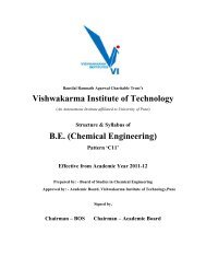
Bansilal Ramnath Agarwal Charitable Trust’s<br />
<strong>Vishwakarma</strong> Institute of Technology, Pune – 411 037<br />
Department of <strong>Electronics</strong> <strong>and</strong> <strong>Telecommunication</strong> <strong>Engineering</strong><br />
FF No.: 654<br />
EC42105:: VLSI DESIGN<br />
Credits: 03<br />
Teaching Scheme: - Theory 3 Hrs/Week<br />
Prerequisites: Nil<br />
Objectives:<br />
• To study concepts of CMOS Analog & Digital Design.<br />
• To be familiar with CMOS fabrication process.<br />
• Mapping with PEOs:2,3,5,6,7,8,9<br />
Unit I: MOSFET SPICE modeling<br />
(8 Hrs)<br />
A. Modeling of semiconductor devices, MOSFET modeling, small signal model for MOS<br />
transistor, Modeling of secondary & short channel effects, sub threshold modeling,<br />
underst<strong>and</strong>ing role of parameters in model, Introduction to industry st<strong>and</strong>ard models like<br />
PSP, Bsim.<br />
B. Surface potential <strong>and</strong> threshold voltage based model.<br />
Unit II: Analog CMOS sub circuits<br />
(8 Hrs)<br />
A. MOS Switch, Calculation of charge feed through error, MOS diode, Current Sink <strong>and</strong><br />
Sources, Designing cascade current sink for a given V min, Designing the self biased high<br />
swing cascade current sink for a given V min, Current Mirrors, Aspect ratio errors in<br />
current amplifiers, Reduction of the aspect ratio error in current amplifier, Current <strong>and</strong><br />
voltage references, B<strong>and</strong>gap reference.<br />
B. Design of a B<strong>and</strong>gap voltage reference.<br />
Unit III: CMOS Amplifier<br />
(8 Hrs)<br />
A. CMOS Amplifiers, Inverters, Active load Inverter, Current Source Inverter, Push pull<br />
inverter, Noise analysis of inverter, Differential amplifier, Large Signal analysis,<br />
Calculation of the worst case input common mode range of the N channel input<br />
differential amplifier, Small signal analysis of differential amplifier, Slew rate <strong>and</strong> noise,<br />
Current source load differential amplifier, Design of a CMOS differential amplifier with<br />
a current mirror as a load.<br />
Structure & Syllabus of B.E (E&TC) Program – Pattern ‘C11’, Rev01, dt. 2/4/2011<br />
53