DS90LV019 3.3V or 5V LVDS Driver/Receiver
DS90LV019 3.3V or 5V LVDS Driver/Receiver
DS90LV019 3.3V or 5V LVDS Driver/Receiver

You also want an ePaper? Increase the reach of your titles
YUMPU automatically turns print PDFs into web optimized ePapers that Google loves.
<strong>DS90LV019</strong><br />
<strong>3.3V</strong> <strong>or</strong> <strong>5V</strong> <strong>LVDS</strong> <strong>Driver</strong>/<strong>Receiver</strong><br />
General Description<br />
The <strong>DS90LV019</strong> is a <strong>Driver</strong>/<strong>Receiver</strong> designed specifically<br />
f<strong>or</strong> the high speed low power point-to-point interconnect applications.<br />
The device operates from a single <strong>3.3V</strong> <strong>or</strong> 5.0V<br />
power supply and includes one differential line driver and<br />
one receiver. The <strong>DS90LV019</strong> features an independent<br />
driver and receiver with TTL/CMOS compatibility (D IN and<br />
R OUT ). The logic interface provides maximum flexibility as 4<br />
separate lines are provided (D IN , DE, RE, and R OUT ). The<br />
device also features a flow-through pin out which allows<br />
easy PCB routing f<strong>or</strong> sh<strong>or</strong>t stubs between its pins and the<br />
connect<strong>or</strong>. The driver has 3.5 mA output loop current.<br />
The driver translates between TTL levels (single-ended) to<br />
Low Voltage Differential Signaling levels. This allows f<strong>or</strong> high<br />
speed operation, while consuming minimal power with reduced<br />
EMI. In addition, the differential signaling provides<br />
common-mode noise rejection.<br />
The receiver threshold is ±100 mV over a ±1V commonmode<br />
range and translates the low swing differential levels<br />
to standard (TTL/CMOS) levels.<br />
Features<br />
n <strong>LVDS</strong> Signaling<br />
n <strong>3.3V</strong> <strong>or</strong> 5.0V operation<br />
n Low power CMOS design<br />
n Balanced Output Impedance<br />
n Glitch free power up/down (<strong>Driver</strong> disabled)<br />
n High Signaling Rate Capacity (above 100 Mbps)<br />
n Ultra Low Power Dissipation<br />
n ±1V Common-Mode Range<br />
n ±100 mV <strong>Receiver</strong> Sensitivity<br />
n Product offered in SOIC and TSSOP packages<br />
n Flow-Through Pin Out<br />
n Industrial Temperature Range Operation<br />
August 2000<br />
<strong>DS90LV019</strong> <strong>3.3V</strong> <strong>or</strong> <strong>5V</strong> <strong>LVDS</strong> <strong>Driver</strong>/<strong>Receiver</strong><br />
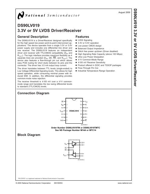
Connection Diagram<br />
Block Diagram<br />
DS100053-1<br />
Order Number <strong>DS90LV019</strong>TM <strong>or</strong> <strong>DS90LV019</strong>TMTC<br />
See NS Package Number M14A <strong>or</strong> MTC14<br />
DS100053-2<br />
TRI-STATE ® is a registered trademark of National Semiconduct<strong>or</strong> C<strong>or</strong>p<strong>or</strong>ation.<br />
© 2000 National Semiconduct<strong>or</strong> C<strong>or</strong>p<strong>or</strong>ation DS100053 www.national.com
<strong>DS90LV019</strong><br />
Absolute Maximum Ratings (Note 1)<br />
If Military/Aerospace specified devices are required,<br />
please contact the National Semiconduct<strong>or</strong> Sales Office/<br />
Distribut<strong>or</strong>s f<strong>or</strong> availability and specifications.<br />
Supply Voltage V CC 6.0V<br />
Enable Input Voltage (DE, RE) −0.3V to (V CC +0.3V)<br />
<strong>Driver</strong> Input Voltage (D IN ) −0.3V to (V CC + 0.3V)<br />
<strong>Receiver</strong> Output Voltage<br />
(R OUT ) −0.3V to (V CC + 0.3V)<br />
<strong>Driver</strong> Output Voltage (DO±)<br />
−0.3V to +3.9V<br />
<strong>Receiver</strong> Input Voltage (RI±) −0.3V to (V CC + 0.3V)<br />
<strong>Driver</strong> Sh<strong>or</strong>t Circuit Current<br />
Continuous<br />
ESD (Note 4)<br />
(HBM, 1.5 kΩ, 100 pF)<br />
> 2.0 kV<br />
(EIAJ, 0 Ω, 200 pF)<br />
> 200 V<br />
Maximum Package Power Dissipation at 25˚C<br />
SOIC<br />
960 mW<br />
Derate SOIC Package<br />
TSSOP<br />
Derate TSSOP Package<br />
St<strong>or</strong>age Temperature Range<br />
Lead Temperature<br />
(Soldering, 4 sec.)<br />
Recommended Operating<br />
Conditions<br />
7.7mW/˚C<br />
790 mW<br />
6.3mW/˚C<br />
−65˚C to +150˚C<br />
260˚C<br />
Min Max Units<br />
Supply Voltage (V CC ) <strong>or</strong> 3.0 3.6 V<br />
Supply Voltage (V CC ) 4.5 5.5 V<br />
<strong>Receiver</strong> Input Voltage 0.0 2.4 V<br />
Operating Free Air<br />
Temperature T A −40 +85 ˚C<br />
DC Electrical Characteristics<br />
T A = −40˚C to +85˚C unless otherwise noted, V CC = 3.3 ± 0.3V. (Notes 2, 3)<br />
Symbol Parameter Conditions Pin Min Typ Max Units<br />
DIFFERENTIAL DRIVER CHARACTERISTICS<br />
V OD Output Differential Voltage R L = 100Ω (Figure 1) DO+, 250 350 450 mV<br />
∆V OD V OD Magnitude Change DO−<br />
6 60 mV<br />
V OS Offset Voltage 1 1.25 1.7 V<br />
∆V OS Offset Magnitude Change 5 60 mV<br />
I OZD TRI-STATE ® Leakage V OUT =V CC <strong>or</strong> GND, DE = 0V −10 ±1 +10 µA<br />
I OXD Power-Off Leakage V OUT = 3.6V <strong>or</strong> GND, V CC = 0V −10 ±1 +10 µA<br />
I OSD Output Sh<strong>or</strong>t Circuit Current V OUT = 0V, DE = V CC −10 −6 −4 mA<br />
DIFFERENTIAL RECEIVER CHARACTERISTICS<br />
V OH Voltage Output High VID = +100 mV I OH = −400 µA R OUT 2.9 3.3 V<br />
Inputs Open 2.9 3.3 V<br />
V OL Voltage Output Low I OL = 2.0 mA, VID = −100 mV 0.1 0.4 V<br />
I OS Output Sh<strong>or</strong>t Circuit Current V OUT = 0V −75 −34 −20 mA<br />
V TH Input Threshold High RI+,<br />
+100 mV<br />
V TH Input Threshold Low RI− −100 mV<br />
I IN Input Current V IN = +2.4V <strong>or</strong> 0V, V CC = 3.6V <strong>or</strong><br />
−10 ±1 +10 µA<br />
0V<br />
DEVICE CHARACTERISTICS<br />
V IH Minimum Input High Voltage D IN , 2.0 V CC V<br />
V IL Maximum Input Low Voltage DE, RE GND 0.8 V<br />
I IH Input High Current V IN =V CC <strong>or</strong> 2.4V ±1 ±10 µA<br />
I IL Input Low Current V IN = GND <strong>or</strong> 0.4V ±1 ±10 µA<br />
V CL Input Diode Clamp Voltage I CLAMP = −18 mA −1.5 −0.7 V<br />
I CCD Power Supply Current DE = RE = V CC V CC 9 12.5 mA<br />
I CCR DE=RE=0V 4.5 7.0 mA<br />
I CCZ DE = 0V, RE = V CC 3.7 7.0 mA<br />
I CC DE=V CC ,RE=0V 15 20 mA<br />
C D output Capacitance DO+,<br />
5 pF<br />
DO−<br />
C R input Capacitance RI+,<br />
RI−<br />
5 pF<br />
www.national.com 2
DC Electrical Characteristics<br />
T A = −40˚C to +85˚C unless otherwise noted, V CC = 5.0 ± 0.<strong>5V</strong>. (Notes 2, 3)<br />
Symbol Parameter Conditions Pin Min Typ Max Units<br />
DIFFERENTIAL DRIVER CHARACTERISTICS<br />
V OD Output Differential Voltage R L = 100Ω (Figure 1) DO+, 250 360 450 mV<br />
∆V OD V OD Magnitude Change DO−<br />
6 60 mV<br />
V OS Offset Voltage 1 1.25 1.8 V<br />
∆V OS Offset Magnitude Change 5 60 mV<br />
I OZD TRI-STATE Leakage V OUT =V CC <strong>or</strong> GND, DE = 0V −10 ±1 +10 µA<br />
I OXD Power-Off Leakage V OUT = 5.<strong>5V</strong> <strong>or</strong> GND, V CC = 0V −10 ±1 +10 µA<br />
I OSD Output Sh<strong>or</strong>t Circuit Current V OUT = 0V, DE = V CC −10 −6 −4 mA<br />
DIFFERENTIAL RECEIVER CHARACTERISTICS<br />
V OH Voltage High VID = +100 mV I OH = −400 µA R OUT 4.3 5.0 V<br />
Inputs Open 4.3 5.0 V<br />
V OL Voltage Output Low I OL = 2.0 mA, VID = −100 mV 0.1 0.4 V<br />
I OS Output Sh<strong>or</strong>t Circuit Current V OUT = 0V −150 −75 −40 mA<br />
V TH Input Threshold High RI+,<br />
+100 mV<br />
V TH Input Threshold Low RI− −100 mV<br />
I IN Input Current V IN = +2.4V <strong>or</strong> 0V, V CC = 5.<strong>5V</strong> <strong>or</strong><br />
−15 ±1 +15 µA<br />
0V<br />
DEVICE CHARACTERISTICS<br />
V IH Minimum Input High Voltage D IN , 2.0 V CC V<br />
V IL Maximum Input Low Voltage DE ,RE GND 0.8 V<br />
I IH Input High Current V IN =V CC <strong>or</strong> 2.4 V ±1 ±10 µA<br />
I IL Input Low Current V IN = GND <strong>or</strong> 0.4V ±1 ±10 µA<br />
V CL Input Diode Clamp Voltage I CLAMP = −18 mA −1.5 −0.8 V<br />
I CCD Power Supply Current DE = RE = V CC V CC 12 19 mA<br />
I CCR DE=RE=0V 5.8 8 mA<br />
I CCZ DE = 0V, RE = V CC 4.5 8.5 mA<br />
I CC DE=V CC ,RE=0V 18 48 mA<br />
C D output Capacitance DO+,<br />
5 pF<br />
DO−<br />
C R input Capacitance RI+,<br />
RI−<br />
5 pF<br />
Note 1: “Absolute Maximum Ratings” are these beyond which the safety of the device cannot be guaranteed. They are not meant to imply that the device should<br />
be operated at these limits. The table of “Electrical Characteristics” provides conditions f<strong>or</strong> actual device operation.<br />
Note 2: All currents into device pins are positive; all currents out of device pins are negative. All voltages are referenced to device ground unless otherwise specified.<br />
Note 3: All typicals are given f<strong>or</strong> V CC = +<strong>3.3V</strong> <strong>or</strong> +5.0V and T A = +25˚C, unless otherwise stated.<br />
Note 4: ESD Rating:<br />
HBM (1.5 kΩ, 100 pF) > 2.0 kV<br />
EIAJ (0Ω, 200 pF) > 200V.<br />
Note 5: C L includes probe and fixture capacitance.<br />
Note 6: Generat<strong>or</strong> wavef<strong>or</strong>ms f<strong>or</strong> all tests unless otherwise specified; f=1MHz, Z O =50Ω,t r =t f ≤6.0 ns (0%–100%).<br />
<strong>DS90LV019</strong><br />
AC Electrical Characteristics<br />
T A = −40˚C to +85˚C, V CC = <strong>3.3V</strong> ± 0.3V. (Note 6)<br />
Symbol Parameter Conditions Min Typ Max Units<br />
DRIVER TIMING REQUIREMENTS<br />
t PHLD Differential Propagation Delay High to Low R L = 100Ω,<br />
2.0 4.0 6.5 ns<br />
t PLHD Differential Propagation Delay Low to High C L =10pF<br />
1.0 5.6 7.0 ns<br />
t SKD Differential Skew |t PHLD −t PLHD |<br />
(Figure 2 and Figure 3)<br />
0.4 1.0 ns<br />
t TLH Transition Time Low to High 0.2 0.7 3.0 ns<br />
t THL Transition Time High to Low 0.2 0.8 3.0 ns<br />
3<br />
www.national.com
<strong>DS90LV019</strong><br />
AC Electrical Characteristics (Continued)<br />
T A = −40˚C to +85˚C, V CC = <strong>3.3V</strong> ± 0.3V. (Note 6)<br />
Symbol Parameter Conditions Min Typ Max Units<br />
DRIVER TIMING REQUIREMENTS<br />
t PHZ Disable Time High to Z R L = 100Ω,<br />
1.5 4.0 8.0 ns<br />
t PLZ Disable Time Low to Z C L =10pF<br />
2.5 5.3 9.0 ns<br />
t PZH Enable Time Z to High<br />
(Figure 4 and Figure 5)<br />
4.0 6.0 8.0 ns<br />
t PZL Enable Time Z to Low 3.5 6.0 8.0 ns<br />
RECEIVER TIMING REQUIREMENTS<br />
t PHLD Differential Propagation Delay High to Low C L =10pF,<br />
3.0 5.8 7.0 ns<br />
t PLHD Differential Propagation Delay Low to High VID = 200 mV<br />
3.0 5.6 9.0 ns<br />
t SKD Differential Skew |t PHLD −t PLHD |<br />
(Figure 6 and Figure 7)<br />
0.55 1.5 ns<br />
t r Rise Time 0.15 2.0 3.0 ns<br />
t f Fall Time 0.15 0.9 3.0 ns<br />
t PHZ Disable Time High to Z R L = 500Ω,<br />
3.0 4.0 6.0 ns<br />
t PLZ Disable Time Low to Z C L =10pF<br />
3.0 4.5 6.0 ns<br />
t PZH Enable Time Z to High<br />
(Figure 8 and Figure 9)<br />
3.0 6.0 8.0 ns<br />
t PZL Enable Time Z to Low 3.0 6.0 8.0 ns<br />
AC Electrical Characteristics<br />
T A = −40˚C to +85˚C, V CC = 5.0V ± 0.<strong>5V</strong>. (Note 6)<br />
Symbol Parameter Conditions Min Typ Max Units<br />
DRIVER TIMING REQUIREMENTS<br />
t PHLD Differential Propagation Delay High to Low R L = 100Ω,<br />
2.0 3.3 6.0 ns<br />
t PLHD Differential Propagation Delay Low to High C L =10pF<br />
1.0 3.3 5.0 ns<br />
t SKD Differential Skew |t PHLD −t PLHD |<br />
(Figure 2 and Figure 3)<br />
0.6 1.0 ns<br />
t TLH Transition Time Low to High 0.15 0.9 3.0 ns<br />
t THL Transition Time High to Low 0.15 1.2 3.0 ns<br />
t PHZ Disable Time High to Z R L = 100Ω,<br />
1.5 3.5 7.0 ns<br />
t PLZ Disable Time Low to Z C L =10pF<br />
3.0 5.2 9.0 ns<br />
t PZH Enable Time Z to High<br />
(Figure 4 and Figure 5)<br />
2.0 4.5 7.0 ns<br />
t PZL Enable Time Z to Low 2.0 4.5 7.0 ns<br />
RECEIVER TIMING REQUIREMENTS<br />
t PHLD Differential Propagation Delay High to Low C L =10pF,<br />
3.0 6.0 8.0 ns<br />
t PLHD Differential Propagation Delay Low to High VID = 200 mV<br />
3.0 5.6 8.0 ns<br />
t SKD Differential Skew |t PHLD −t PLHD |<br />
(Figure 6 and Figure 7)<br />
0.7 1.6 ns<br />
t r Rise Time 0.15 0.8 3.0 ns<br />
t f Fall Time 0.15 0.8 3.0 ns<br />
t PHZ Disable Time High to Z R L = 500Ω,<br />
3.0 3.5 4.5 ns<br />
t PLZ Disable Time Low to Z C L =10pF<br />
3.5 3.6 7.0 ns<br />
t PZH Enable Time Z to High<br />
(Figure 8 and Figure 9)<br />
3.0 5.0 7.0 ns<br />
t PZL Enable Time Z to Low 3.0 5.0 7.0 ns<br />
www.national.com 4
Test Circuits and Timing Wavef<strong>or</strong>ms<br />
<strong>DS90LV019</strong><br />
FIGURE 1. Differential <strong>Driver</strong> DC Test Circuit<br />
DS100053-3<br />
DS100053-4<br />
FIGURE 2. Differential <strong>Driver</strong> Propagation Delay and Transition Test Circuit<br />
DS100053-5<br />
FIGURE 3. Differential <strong>Driver</strong> Propagation and Transition Time Wavef<strong>or</strong>ms<br />
FIGURE 4. <strong>Driver</strong> TRI-STATE Delay Test Circuit<br />
DS100053-6<br />
5<br />
www.national.com
<strong>DS90LV019</strong><br />
Test Circuits and Timing Wavef<strong>or</strong>ms (Continued)<br />
FIGURE 5. <strong>Driver</strong> TRI-STATE Delay Wavef<strong>or</strong>ms<br />
DS100053-7<br />
DS100053-8<br />
FIGURE 6. <strong>Receiver</strong> Propagation Delay and Transition Time Test Circuit<br />
FIGURE 7. <strong>Receiver</strong> Propagation Delay and Transition Time Wavef<strong>or</strong>ms<br />
DS100053-9<br />
FIGURE 8. <strong>Receiver</strong> TRI-STATE Delay Test Circuit<br />
DS100053-10<br />
www.national.com 6
Test Circuits and Timing Wavef<strong>or</strong>ms (Continued)<br />
<strong>DS90LV019</strong><br />
FIGURE 9. <strong>Receiver</strong> TRI-STATE Delay Wavef<strong>or</strong>ms TRI-STATE Delay Wavef<strong>or</strong>ms<br />
DS100053-11<br />
DS100053-13<br />
FIGURE 10. Terminated Input Fail-Safe Circuit<br />
Typical Application Diagram<br />
Applications Inf<strong>or</strong>mation<br />
The <strong>DS90LV019</strong> has two control pins, which allows the device<br />
to operate as a driver, a receiver <strong>or</strong> both driver and a receiver<br />
at the same time. There are a few common practices<br />
which should be implied when designing PCB f<strong>or</strong> <strong>LVDS</strong> signaling.<br />
Recommended practices are:<br />
• Use at least 4 PCB board layer (<strong>LVDS</strong> signals, ground,<br />
power and TTL signals).<br />
• Keep drivers and receivers as close to the (<strong>LVDS</strong> p<strong>or</strong>t<br />
side) connect<strong>or</strong> as possible.<br />
• Bypass each <strong>LVDS</strong> device and also use distributed bulk<br />
capacitance. Surface mount capacit<strong>or</strong>s placed close to<br />
power and ground pins w<strong>or</strong>k best. Two <strong>or</strong> three multilayer<br />
ceramic (MLC) surface mount capacit<strong>or</strong>s 0.1 µF,<br />
DS100053-12<br />
and 0.01 µF in parallel should be used between each V CC<br />
and ground. The capacit<strong>or</strong>s should be as close as possible<br />
to the V CC pin.<br />
• Use controlled impedance traces which match the differential<br />
impedance of your transmission medium (i.e.,<br />
Cable) and termination resist<strong>or</strong>.<br />
• Use the termination resist<strong>or</strong> which best matches the differential<br />
impedance of your transmission line.<br />
• Isolate TTL signals from <strong>LVDS</strong> signals.<br />
MEDIA (CABLE AND CONNECTOR) SELECTION:<br />
• Use controlled impedance media. The cables and connect<strong>or</strong>s<br />
should have a matched differential impedance of<br />
about 100Ω.<br />
7<br />
www.national.com
<strong>DS90LV019</strong><br />
Applications Inf<strong>or</strong>mation (Continued)<br />
• Balanced cables (e.g., twisted pair) are usually better<br />
than unbalanced cables (ribbon cable, simple coax) f<strong>or</strong><br />
noise reduction and signal quality.<br />
• F<strong>or</strong> cable distances < 0.5m, most cables can be made to<br />
w<strong>or</strong>k effectively. F<strong>or</strong> distances 0.5m ≤ d ≤ 10m, CAT 3<br />
(categ<strong>or</strong>y 3) twisted pair cable w<strong>or</strong>ks well and is readily<br />
available and relatively inexpensive. F<strong>or</strong> distances<br />
> 10m, and high data rates CAT 5 twisted pair is recommended.<br />
• There are three Fail-Safe scenarios, open input pins,<br />
sh<strong>or</strong>ted inputs pins and terminated input pins. The first<br />
case is guaranteed f<strong>or</strong> <strong>DS90LV019</strong>. A HIGH state on<br />
R OUT pin can be achieved by using two external resist<strong>or</strong>s<br />
(one to V CC and one to GND) per Figure 10 (Terminated<br />
Input Fail-Safe Circuit). R1 and R2 should be R T to limit<br />
the loading to the <strong>LVDS</strong> driver . R T is selected to match<br />
the impedance of the cable.<br />
TABLE 1. Functional Table<br />
MODE SELECTED DE RE<br />
DRIVER MODE H H<br />
RECEIVER MODE L L<br />
TRI-STATE MODE L H<br />
FULL DUPLEX MODE H L<br />
TABLE 2. Transmitter Mode<br />
INPUTS<br />
OUTPUTS<br />
DE DI DO+ DO−<br />
H L L H<br />
H H H L<br />
H 2 > & > 0.8 X X<br />
L X Z Z<br />
X = High <strong>or</strong> Low logic state<br />
Z = High impedance state<br />
L = Low state<br />
H = High state<br />
TABLE 3. <strong>Receiver</strong> Mode<br />
INPUTS<br />
OUTPUT<br />
RE<br />
(RI+) − (RI−)<br />
L L (< −100 mV) L<br />
L H (> +100 mV) H<br />
L 100 mV > & > −100 mV X<br />
H X Z<br />
X = High <strong>or</strong> Low logic state<br />
Z = High impedance state<br />
L = Low state<br />
H = High state<br />
TABLE 4. Device Pin Description<br />
Pin Name Pin # Input/Output Description<br />
D IN 2 I TTL <strong>Driver</strong> Input<br />
DO± 11, 12 O <strong>LVDS</strong> <strong>Driver</strong> Outputs<br />
RI± 9, 10 I <strong>LVDS</strong> <strong>Receiver</strong> Inputs<br />
R OUT 4 O TTL <strong>Receiver</strong> Output<br />
RE 8 I <strong>Receiver</strong> Enable TTL Input (Active Low)<br />
DE 1 I <strong>Driver</strong> Enable TTL Input (Active High)<br />
GND 7 NA Ground<br />
V CC 14 NA Power Supply (<strong>3.3V</strong> ± 0.3V <strong>or</strong> 5.0V ± 0.<strong>5V</strong>)<br />
www.national.com 8
Physical Dimensions inches (millimeters) unless otherwise noted<br />
<strong>DS90LV019</strong><br />
Order Number <strong>DS90LV019</strong>TM<br />
NS Package Number M14A<br />
9<br />
www.national.com
<strong>DS90LV019</strong> <strong>3.3V</strong> <strong>or</strong> <strong>5V</strong> <strong>LVDS</strong> <strong>Driver</strong>/<strong>Receiver</strong><br />
Physical Dimensions inches (millimeters) unless otherwise noted (Continued)<br />
Order Number <strong>DS90LV019</strong>TMTC<br />
NS Package Number MTC14<br />
LIFE SUPPORT POLICY<br />
NATIONAL’S PRODUCTS ARE NOT AUTHORIZED FOR USE AS CRITICAL COMPONENTS IN LIFE SUPPORT<br />
DEVICES OR SYSTEMS WITHOUT THE EXPRESS WRITTEN APPROVAL OF THE PRESIDENT AND GENERAL<br />
COUNSEL OF NATIONAL SEMICONDUCTOR CORPORATION. As used herein:<br />
1. Life supp<strong>or</strong>t devices <strong>or</strong> systems are devices <strong>or</strong><br />
systems which, (a) are intended f<strong>or</strong> surgical implant<br />
into the body, <strong>or</strong> (b) supp<strong>or</strong>t <strong>or</strong> sustain life, and<br />
whose failure to perf<strong>or</strong>m when properly used in<br />
acc<strong>or</strong>dance with instructions f<strong>or</strong> use provided in the<br />
labeling, can be reasonably expected to result in a<br />
significant injury to the user.<br />
2. A critical component is any component of a life<br />
supp<strong>or</strong>t device <strong>or</strong> system whose failure to perf<strong>or</strong>m<br />
can be reasonably expected to cause the failure of<br />
the life supp<strong>or</strong>t device <strong>or</strong> system, <strong>or</strong> to affect its<br />
safety <strong>or</strong> effectiveness.<br />
National Semiconduct<strong>or</strong><br />
C<strong>or</strong>p<strong>or</strong>ation<br />
Americas<br />
Tel: 1-800-272-9959<br />
Fax: 1-800-737-7018<br />
Email: supp<strong>or</strong>t@nsc.com<br />
www.national.com<br />
National Semiconduct<strong>or</strong><br />
Europe<br />
Fax: +49 (0) 180-530 85 86<br />
Email: europe.supp<strong>or</strong>t@nsc.com<br />
Deutsch Tel: +49 (0) 69 9508 6208<br />
English Tel: +44 (0) 870 24 0 2171<br />
Français Tel: +33 (0) 1 41 91 8790<br />
National Semiconduct<strong>or</strong><br />
Asia Pacific Customer<br />
Response Group<br />
Tel: 65-2544466<br />
Fax: 65-2504466<br />
Email: ap.supp<strong>or</strong>t@nsc.com<br />
National Semiconduct<strong>or</strong><br />
Japan Ltd.<br />
Tel: 81-3-5639-7560<br />
Fax: 81-3-5639-7507<br />
National does not assume any responsibility f<strong>or</strong> use of any circuitry described, no circuit patent licenses are implied and National reserves the right at any time without notice to change said circuitry and specifications.