DG8SAQ VNWA Kit Assembly Manual - SDR-Kits
DG8SAQ VNWA Kit Assembly Manual - SDR-Kits
DG8SAQ VNWA Kit Assembly Manual - SDR-Kits

Create successful ePaper yourself
Turn your PDF publications into a flip-book with our unique Google optimized e-Paper software.
<strong>SDR</strong>-<strong>Kit</strong>s.net <strong>DG8SAQ</strong> USB-<strong>VNWA</strong> 1.1, 1.2 & 1.3 <strong>Assembly</strong> <strong>Manual</strong> 1.3a<br />
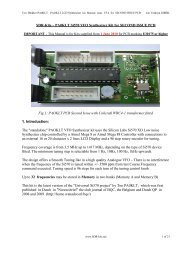
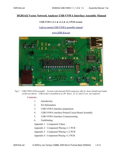
<strong>DG8SAQ</strong> Vector Network Analyser USB-<strong>VNWA</strong> Interface <strong>Assembly</strong> <strong>Manual</strong><br />
USB-<strong>VNWA</strong> v1.1 & v1.2 & v1.3 PCB version<br />
Link to current USB-<strong>VNWA</strong> assembly manual<br />
www.<strong>SDR</strong>-<strong>Kit</strong>s.net<br />
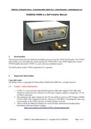
Fig 1:<br />
USB-<strong>VNWA</strong> PCB assembly – Version with internal PCB connectors (<strong>Kit</strong> 4) hence Dsub9 and Audio<br />
socket not shown. USB socket is installed in as J9, hence J3, L1 and L2 are not required<br />
Contents:<br />
1. Introduction<br />
2. <strong>Kit</strong> Information<br />
3. USB-<strong>VNWA</strong> Interface preparation<br />
4. USB-<strong>VNWA</strong> interface Printed Circuit Board <strong>Assembly</strong><br />
5. USB-<strong>VNWA</strong> Interface Commissioning<br />
6. Faultfinding<br />
Appendix 1 – Component Values<br />
Appendix 2 – Component Placing v1.1 PCB<br />
Appendix 3 – Component Placing v1.2 PCB<br />
Appendix 4 - Component Placing v1.3 PCB<br />
<strong>SDR</strong>-<strong>Kit</strong>s.net © 2009 by Jan Verduyn G0BBL <strong>SDR</strong>-<strong>Kit</strong>s & Thomas Baier <strong>DG8SAQ</strong> 1 of 29
<strong>SDR</strong>-<strong>Kit</strong>s.net <strong>DG8SAQ</strong> USB-<strong>VNWA</strong> 1.1, 1.2 & 1.3 <strong>Assembly</strong> <strong>Manual</strong> 1.3a<br />
1. INTRODUCTION<br />
The Vector Network Analyser (<strong>VNWA</strong>) described by Thomas Baier <strong>DG8SAQ</strong> in his article “A Small,<br />
Simple, USB-Powered Vector Network Analyser Covering 1 kHz to 1.3 GHz in QEX<br />
January/February 2009 is orginally controlled via the Parallel port of the Personal Computer.<br />
This new add-on USB-<strong>VNWA</strong> Interface card was developed by Tom to allow control of the <strong>VNWA</strong><br />
from the Personal Computer via the popular USB Bus. The USB-<strong>VNWA</strong> interface PCB contains a<br />
USB hub device to extend the USB bus to the PCM2900 Audio Chip and the AtMega88 Controller<br />
chip on the PCB. There are two options:<br />
• For those who already have built and use the <strong>VNWA</strong> PCB fitted with DB9 connector:<br />
The USB-<strong>VNWA</strong> is connected to the <strong>VNWA</strong> PCB assembly via a D9sub connectors through<br />
which <strong>VNWA</strong> +5V Power and <strong>VNWA</strong> control signals are routed and a short 3.5mm to 3.5mm<br />
stereo cable connects both audio sockets. This routes the <strong>VNWA</strong> Reference and multiplexed<br />
Forward and Reflected Audio signals to the PCM2900 Audio Codec for transmission via the<br />
USB bus to the Personal Computer for subsequent processing.<br />
• Complete USB-Controlled <strong>VNWA</strong> <strong>Kit</strong> 4: introduced in December 2009 (s/n 324 and up) uses<br />
internal Single in Line (SIP) 0.1" connectors to mate these signal between the two PCB<br />
assemblies.<br />
2. KIT INFORMATION:<br />
These USB-<strong>VNWA</strong> <strong>Kit</strong> assembly instructions are applicable to USB-<strong>VNWA</strong> v1.1, v1.2 and v1.3<br />
PCB size 98mm x 62mm – same size as <strong>VNWA</strong> PCB.<br />
There are no practical differences between USB-<strong>VNWA</strong> Interface v1.1 and v1.2 Printed<br />
Circuit boards, except that v1.2 has R41 and R42 eliminated and has two minor mechanical<br />
changes in preparation for producing an assembled <strong>VNWA</strong> version later in 2009. Appendix 2<br />
has v1.1 component placing whilst Appendix 3 has the v1.2 PCB component layout.<br />
V1.3 PCB has LED D1 is reversed and the location of R1 has changed. Appendix 4 has<br />
component placing for this PCB version<br />
A <strong>VNWA</strong> Enclosure is available which allows both PCBs to be fitted on top of each other.<br />
Operational Specification<br />
• Power Supply: Powered from +5V 500mA Power Supply or directly from Personal Computer<br />
USB port capable of sourcing 500mA.<br />
• Personal Computer with minimum 1GHz processor and minimum of 64 Mbyte memory<br />
recommended and USB V1.1 or V2.0 connectors and a standard sound card under Microsoft<br />
XP, Vista Home edition or Windows 2000 Operating System. Installation of <strong>DG8SAQ</strong><br />
Firmware Drivers and <strong>DG8SAQ</strong> <strong>VNWA</strong> USB Software Application required.<br />
<strong>SDR</strong>-<strong>Kit</strong>s.net © 2009 by Jan Verduyn G0BBL <strong>SDR</strong>-<strong>Kit</strong>s & Thomas Baier <strong>DG8SAQ</strong> 2 of 29
<strong>SDR</strong>-<strong>Kit</strong>s.net <strong>DG8SAQ</strong> USB-<strong>VNWA</strong> 1.1, 1.2 & 1.3 <strong>Assembly</strong> <strong>Manual</strong> 1.3a<br />
Note: The <strong>VNWA</strong> application has been successfully operated on Pentium III Laptop with 600<br />
MHz Processor, operation on computers with lower specification cannot be guaranteed.<br />
USB-<strong>VNWA</strong> Interface <strong>Kit</strong> Support<br />
Please use the <strong>DG8SAQ</strong> <strong>VNWA</strong> reflector to check for announcements, documentation<br />
updates and to share your experiences building and using the <strong>DG8SAQ</strong> <strong>VNWA</strong>.<br />
http://groups.yahoo.com/group/<strong>VNWA</strong>/<br />
Please contact Jan (email: sdrkits@gmail.com ) for kit hardware issues, short shipments<br />
and Tom to report any software bugs.<br />
<strong>Kit</strong> <strong>Assembly</strong> <strong>Manual</strong> Errors and updates<br />
No responsibility is assumed for any errors in this document. All information is given in good<br />
faith based on information gathered from <strong>Kit</strong> builders.<br />
If you become aware of any errors or have any suggestions to improve the information in this<br />
document please email Jan G0BBL via sdrkits@gmail.com New Document revisions will be<br />
announced in the <strong>VNWA</strong> group and are available from the www.<strong>SDR</strong>-<strong>Kit</strong>s.net Website.<br />
Other Links for Information<br />
<strong>DG8SAQ</strong> <strong>VNWA</strong> Home page: http://www.mydarc.de/dg8saq/<strong>VNWA</strong>21/index.html<br />
<strong>SDR</strong>-<strong>Kit</strong>s <strong>VNWA</strong> Home page: http://www.<strong>SDR</strong>-<strong>Kit</strong>s.net/<strong>VNWA</strong>/<br />
Copyright Notice: This project was initiated and designed by Prof. Dr. Thomas Baier<br />
<strong>DG8SAQ</strong>, who holds copyright to this design. Reproduction of the Printed Circuit Board and<br />
the <strong>VNWA</strong> circuit schematic is not permitted without written permission of the copyright<br />
holder. Reverse Engineering and Commercial reproduction is not allowed.<br />
Please see <strong>SDR</strong>-<strong>Kit</strong>s Ordering Terms and Conditions<br />
Acknowledgments USB-<strong>VNWA</strong> project:<br />
Tom - <strong>DG8SAQ</strong> – Concept – PCB Design & USB-<strong>VNWA</strong> Software and firmware<br />
Jan G0BBL – <strong>Kit</strong> Production – <strong>Kit</strong> <strong>Assembly</strong> Documentation -<br />
Big thanks to various USB-<strong>VNWA</strong> Builders for their help and useful comments!!<br />
<strong>SDR</strong>-<strong>Kit</strong>s.net © 2009 by Jan Verduyn G0BBL <strong>SDR</strong>-<strong>Kit</strong>s & Thomas Baier <strong>DG8SAQ</strong> 3 of 29
<strong>SDR</strong>-<strong>Kit</strong>s.net <strong>DG8SAQ</strong> USB-<strong>VNWA</strong> 1.1, 1.2 & 1.3 <strong>Assembly</strong> <strong>Manual</strong> 1.3a<br />
3. USB-<strong>VNWA</strong> interface Preparation<br />
3.1 Introduction:<br />
If you already have assembled the <strong>VNWA</strong> Printed Circuit Board, you will find that the<br />
USB_<strong>VNWA</strong> is somewhat less challenging compared to assemble compared to the <strong>VNWA</strong> ,<br />
however please pay attention especially when soldering the U4 PCM2900 and the U2<br />
TUSB2036 USB Hub. Do NOT fit the 28 pin IC socket until indicated. The 0603<br />
components should be soldered first as space quite tight near the socket.<br />
3.2 Bill of Materials Check:<br />
[ ] Check the contents of the items supplied as shown in Table 1.<br />
Caution: Observe Electro Static Precautions when handling ESD sensitive components. Do not<br />
remove ICs from packaging until required.<br />
<strong>DG8SAQ</strong> USB <strong>VNWA</strong> Control Board v1.1, v1.2 & v1.3 PCB – BOM<br />
ITEM QTY Remark Capacitors QTY Remark<br />
U1, U3 LE33 2 15p 2 red/black<br />
D2, D3 MBR0520 2 B25 27p 4 red/green<br />
U2 TUSB2036 1 1n 4 black<br />
U4 PCM2900 1 100n 19 red stripe<br />
Q1 IRLML6401 1 F8?85 1u 6 blue<br />
D1 LED 1 10u 7<br />
X1 6 MHz 1<br />
X2 12 MHz 1 Resistors<br />
F1 PFRA010 Fuse 1 or XF010 0R 3 0 or 000<br />
L1..L4 Choke 400mA 4.7uH 2 2 fitted 22R 7 22<br />
J26 3 pin 0.1” 1 47R 2 47R<br />
USB_<strong>VNWA</strong> PCB 1 68R 3 68<br />
J3 or J9 USB Socket 1 100R 6 100, 101 01A<br />
J23 USB out Socket 1 680R 3 681<br />
1K 4 102 or 01B<br />
J5 Db9 Male (or 5 & 4 pin SIP) 1 Note 1 1K5 6 152 or 1BB<br />
J24 AUDIO_JACK (or 3 pin SIP) 1 Note 1 10K 5 103 or 01C<br />
Db9 male IDC 1 Note 1 15K 8 153 or 1BC<br />
Db9 female IDC 1 Note 1 150K 2 154 or 1BD<br />
10 core cable 10 cm Note 1 1M 2 105<br />
3.5 mm Plug stereo 2 Note 1<br />
IC socket 28 pin 0.3” 1<br />
I ATMEGA88-16PI 1 Programmed<br />
Circuit Information 1 Copyright<br />
License Key information 1<br />
Note 1: If <strong>VNWA</strong> <strong>Kit</strong> 4 is ordered 3 pcs SIP Male 0.1” connectors (5pin, 4pin and 3pin)<br />
will be supplied instead of the connectors listed as Note 1. The SIP connectors allow<br />
the USB-<strong>VNWA</strong> PCB to mate directly with <strong>VNWA</strong> PCB.<br />
Table 1: Bill of Materials for Production <strong>Kit</strong>s<br />
<strong>SDR</strong>-<strong>Kit</strong>s.net © 2009 by Jan Verduyn G0BBL <strong>SDR</strong>-<strong>Kit</strong>s & Thomas Baier <strong>DG8SAQ</strong> 4 of 29
<strong>SDR</strong>-<strong>Kit</strong>s.net <strong>DG8SAQ</strong> USB-<strong>VNWA</strong> 1.1, 1.2 & 1.3 <strong>Assembly</strong> <strong>Manual</strong> 1.3a<br />
3.3 Printed Circuit Board Preparation<br />
[ ] Check whether your kit contains version contains USB-<strong>VNWA</strong> v1.1, v1.2 or v1.3 PCB If<br />
your version is different check whether you have the correct USB-<strong>VNWA</strong> assembly manual<br />
applicable to your particular PCB version supplied.<br />
Appendix 2 has v1.1 component placing whilst Appendix 3 has the v1.2 PCB component layout<br />
and Appendix 4 has the v1.3 component placing<br />
<strong>SDR</strong>-<strong>Kit</strong>s.net © 2009 by Jan Verduyn G0BBL <strong>SDR</strong>-<strong>Kit</strong>s & Thomas Baier <strong>DG8SAQ</strong> 5 of 29
<strong>SDR</strong>-<strong>Kit</strong>s.net <strong>DG8SAQ</strong> USB-<strong>VNWA</strong> 1.1, 1.2 & 1.3 <strong>Assembly</strong> <strong>Manual</strong> 1.3a<br />
4. USB-<strong>VNWA</strong> Interface Printed Circuit Board <strong>Assembly</strong><br />
[ ] Inspect USB-<strong>VNWA</strong> PCB for rough edges and rasp with fine file if necessary.<br />
[ ] Place PCB on black anti-static mat supplied with <strong>VNWA</strong> PCB and set the soldering<br />
station to 330°C = 630°F<br />
[ ] Caution: Observe ESD precautions and correct orientation in the following 2<br />
steps as shown in Appendix 2 or Appendix 3<br />
[ ] Install U4 PCM2900 – observe dot (pin 1) as shown in Appendix Component<br />
Placing<br />
[ ] Install U2 TUSB2036 – observe dot (pin=1) as shown in Appendix Component<br />
Placing<br />
[ ] Install resistor 0R (marking 0 or 000) R28 R41 (R41 is NOT used on<br />
v1.2 and v1.3 PCB!!)<br />
[ ] Install resistor 22R (marking 22) R2, R3, R17, R18,<br />
R35, R36<br />
[ ] Install resistor 47R (marking 47) R39<br />
[ ] Install resistor 68R (marking 68) R21, R22<br />
[ ] Install resistor 100R (marking 101 or 01A) R29, R30, R31, R32, R33<br />
[ ] Install resistor 680R (marking 681) R38, R40<br />
[ ] Install resistor 1K (marking 102 or 01B) R1, R7, R34<br />
[ ] Install resistor 1K5 (marking 152 or 1BB) R5, R6, R19, R26,<br />
[ ] Install resistor 10K (marking 103 or 01C) R23, R27, R37<br />
[ ] Install resistor 15K (marking 153 or 1BC) R10, R11, R12, R13, R14<br />
R15, R16<br />
[ ] Install resistor 150K (marking 154 or 1BD) R8<br />
[ ] Install resistor 1M (marking 105 or 01E) R20<br />
[ ] Install capacitors (1uF 0805 blue) C20, C21, C22, C23, C36,<br />
<strong>SDR</strong>-<strong>Kit</strong>s.net © 2009 by Jan Verduyn G0BBL <strong>SDR</strong>-<strong>Kit</strong>s & Thomas Baier <strong>DG8SAQ</strong> 6 of 29
<strong>SDR</strong>-<strong>Kit</strong>s.net <strong>DG8SAQ</strong> USB-<strong>VNWA</strong> 1.1, 1.2 & 1.3 <strong>Assembly</strong> <strong>Manual</strong> 1.3a<br />
[ ] Install capacitors (100nF 0603 red) C2, C4, C6, C8, C10,<br />
C12, C15, C16, C17, C24,<br />
C25, C26, C29, C32, C33,<br />
C34, C37, C38<br />
[ ] Install capacitors (1nF 0603 black) C5, C31, C35<br />
[ ] Install capacitors (27pF 0603 red/green) C3, C7, C27<br />
[ ] Install capacitors (15pF 0603 red/black) C28<br />
[ ] Caution: Observe orientation as shown in Appendix 2 or 3 (black stripe or +<br />
symbol) in the following 2 step. (For Tantalum capacitors supplied in the <strong>Kit</strong> the<br />
BLACK STRIPE indicates the + terminal.)<br />
[ ] Install capacitors (10uF) C1, C9, C11, C13, C14,<br />
C18, C19<br />
[ ] Install diodes (MBR020L marking 1B28 or B25) D2, D3<br />
Caution: Observe orientation of black stripe or the letter “c”. Use a 5x magnifier to<br />
detect the small raised edge at one end of the case of the diode, which indicates the<br />
cathode.<br />
[ ] Install LE33 U1, U3<br />
[ ] Install IRLML6401 Q1 (mark F8?85)<br />
[ ] LED D1 (Connect the Anode (Longer lead<br />
to the square pad)<br />
[ ] Crystals X1 (6 MHz) X2 (12 MHz)<br />
[ ] Fuse XF010 or PFRA010 F1<br />
Note:<br />
In the following steps the USB-B connector is installed in position J9 to suit the<br />
<strong>SDR</strong>-<strong>Kit</strong>s <strong>VNWA</strong> Enclosure which has USB connection at the rear. If you require the<br />
USB-B connection on the front panel (not recommended) then install the USB-B<br />
socket provided in position J3 instead of in position J9.<br />
[ ] Install USB-B Connector J9<br />
[ ] Install USB-A Connector J23 (optional connector)<br />
[ ] Choke Inductor 4.7 uH L3, L4 when J9 installed<br />
<strong>SDR</strong>-<strong>Kit</strong>s.net © 2009 by Jan Verduyn G0BBL <strong>SDR</strong>-<strong>Kit</strong>s & Thomas Baier <strong>DG8SAQ</strong> 7 of 29
<strong>SDR</strong>-<strong>Kit</strong>s.net <strong>DG8SAQ</strong> USB-<strong>VNWA</strong> 1.1, 1.2 & 1.3 <strong>Assembly</strong> <strong>Manual</strong> 1.3a<br />
Alternatively as L1, L2 when J3 installed<br />
[ ] Install 3 pin connector J26 (Optional for S-parameter control)<br />
[ ] Install 28 pin DIL IC Socket Caution Observe notch is located<br />
as per Appendix 2 or 3. (points toward<br />
X2)<br />
Caution:<br />
In the next step either DB9 connectors or SIP connectors are installed depending<br />
whether connections with <strong>VNWA</strong> PCB is internal (SIP) or external (DB9)<br />
[ ] Install correct type of connectors for J5 (either DB9 Male or 5 pin and 4 pin male SIP)<br />
[ ] Install correct type of connector for J24 (Audio Connector) (3.5mm Audio socket<br />
or 3 pin male SIP)<br />
Caution: Observe orientation in Appendix 2 or 3 in the following step<br />
[ ] Install programmed controller Atmega88 in 28 pin socket I1 so notch points to X2<br />
[ ] This completes PCB assembly. check all components and joints with x3<br />
magnification<br />
Note:<br />
D4, D5 and R42 is not installed on v1.1 PCB and higher.<br />
R41 is not present on v1.2 and v1.3 PCB. (0 Ohm replaced by track)<br />
<strong>SDR</strong>-<strong>Kit</strong>s.net © 2009 by Jan Verduyn G0BBL <strong>SDR</strong>-<strong>Kit</strong>s & Thomas Baier <strong>DG8SAQ</strong> 8 of 29
<strong>SDR</strong>-<strong>Kit</strong>s.net <strong>DG8SAQ</strong> USB-<strong>VNWA</strong> 1.1, 1.2 & 1.3 <strong>Assembly</strong> <strong>Manual</strong> 1.3a<br />
5.0 USB-<strong>VNWA</strong> Commissioning and Final <strong>Assembly</strong><br />
Caution: In the follow step separate instructions are given depending whether external (DB9)<br />
connectors or Internal connectors (SIP) are fitted<br />
5. 1 USB-<strong>VNWA</strong> Interface <strong>Assembly</strong> and Checks (External Connections DB9 connectors)<br />
Introduction: Commissioning the USB-<strong>VNWA</strong> PCB assumes that the <strong>VNWA</strong> PCB fitted<br />
with DB9 Socket has already been commissioned and is fully operational using the Parallel<br />
port interface. If this is not the case then<br />
[ ] Perform the following checks on your <strong>VNWA</strong> board for compatibility<br />
1) If fitted check whether R97, R98, R99, R100 and R101 are 0 Ohms. If not replace by 0<br />
Ohm (wire) link<br />
2) Check whether R52 = 150K (marking1BD) R52 is fitted between pin 1 and pin 2 of U23<br />
[ ] Plug the USB-<strong>VNWA</strong> Interface card into the D9sub Connector of the <strong>VNWA</strong> PCB assembly<br />
[ ] Use a audio cable with 3.5mm stereo plugs on either end to connect <strong>VNWA</strong> Audio socket to<br />
the USB-<strong>VNWA</strong> Audio socket<br />
5.2 <strong>Kit</strong> 4 <strong>VNWA</strong> PCB and USB-<strong>VNWA</strong> <strong>Assembly</strong> (Internal Connections SIL)<br />
[ ] Fit 3 pcs 8mm spacer on the <strong>VNWA</strong> PCB assembly. The correct sequence is:<br />
3mm 6mm long plastic screw, nylon washer, <strong>VNWA</strong> PCB, nylon washer and 8mm spacer.<br />
[ ] Carefully mate the USB-VWA PCB into the <strong>VNWA</strong> as shown in Fig 2. below. Fit nylon<br />
washer and 12.7 mm threaded spacer both sides of J5. Fit nylon and a 3mm plastic screw into<br />
the spacer under the 3rd hole.<br />
<strong>SDR</strong>-<strong>Kit</strong>s.net © 2009 by Jan Verduyn G0BBL <strong>SDR</strong>-<strong>Kit</strong>s & Thomas Baier <strong>DG8SAQ</strong> 9 of 29
<strong>SDR</strong>-<strong>Kit</strong>s.net <strong>DG8SAQ</strong> USB-<strong>VNWA</strong> 1.1, 1.2 & 1.3 <strong>Assembly</strong> <strong>Manual</strong> 1.3a<br />
fig 2: <strong>VNWA</strong> <strong>Kit</strong> 4 (internal connections) PCB mounting detail<br />
5.3 DRIVER INSTALLATION FOR WINDOWS XP<br />
Introduction: In this section a driver needs to be installed on your Personal Computer in order<br />
to recognize your <strong>VNWA</strong>. Note: Only 32 bits Windows Operating Systems<br />
are supported at the present time because Microsoft requires Digitally signed Drivers<br />
for their 64 bit OS.<br />
Caution: Do Not connect the <strong>VNWA</strong> to your personal computer when installing the Driver.<br />
[ ] Download the Drivers from:<br />
http://sdr-kits.net/<strong>VNWA</strong>/USB-<strong>VNWA</strong>/AVR-USB-Driver.zip<br />
[ ] Unpack the Drivers as shown in Fig 3. A directory "AVR-USB-Driver" should be visible with<br />
the files as shown.<br />
<strong>SDR</strong>-<strong>Kit</strong>s.net © 2009 by Jan Verduyn G0BBL <strong>SDR</strong>-<strong>Kit</strong>s & Thomas Baier <strong>DG8SAQ</strong> 10 of 29
<strong>SDR</strong>-<strong>Kit</strong>s.net <strong>DG8SAQ</strong> USB-<strong>VNWA</strong> 1.1, 1.2 & 1.3 <strong>Assembly</strong> <strong>Manual</strong> 1.3a<br />
fig 3: AVR-USB-Driver and Driver files shown after unpacking<br />
[ ] Connect the <strong>VNWA</strong> to the Personal Computer USB socket with a USB cable.<br />
A message will be displayed:<br />
After about 5 seconds the message below should be displayed<br />
<strong>SDR</strong>-<strong>Kit</strong>s.net © 2009 by Jan Verduyn G0BBL <strong>SDR</strong>-<strong>Kit</strong>s & Thomas Baier <strong>DG8SAQ</strong> 11 of 29
<strong>SDR</strong>-<strong>Kit</strong>s.net <strong>DG8SAQ</strong> USB-<strong>VNWA</strong> 1.1, 1.2 & 1.3 <strong>Assembly</strong> <strong>Manual</strong> 1.3a<br />
• Select “No, not this time”<br />
• Press “NEXT”<br />
The following screen should now be displayed:<br />
Deselect “Install the software automatically”<br />
<strong>SDR</strong>-<strong>Kit</strong>s.net © 2009 by Jan Verduyn G0BBL <strong>SDR</strong>-<strong>Kit</strong>s & Thomas Baier <strong>DG8SAQ</strong> 12 of 29
<strong>SDR</strong>-<strong>Kit</strong>s.net <strong>DG8SAQ</strong> USB-<strong>VNWA</strong> 1.1, 1.2 & 1.3 <strong>Assembly</strong> <strong>Manual</strong> 1.3a<br />
Select “install from a list or specific location”<br />
Press “Next>”<br />
The following screen is displayed<br />
• Deselect “Search removable Media”<br />
• Select “Include this location in the search”<br />
• Press “Browse”<br />
• Select Folder AVR-USB-Driver<br />
• Click “Ok”<br />
• Press “Next>”<br />
• Software is being installed<br />
<strong>SDR</strong>-<strong>Kit</strong>s.net © 2009 by Jan Verduyn G0BBL <strong>SDR</strong>-<strong>Kit</strong>s & Thomas Baier <strong>DG8SAQ</strong> 13 of 29
<strong>SDR</strong>-<strong>Kit</strong>s.net <strong>DG8SAQ</strong> USB-<strong>VNWA</strong> 1.1, 1.2 & 1.3 <strong>Assembly</strong> <strong>Manual</strong> 1.3a<br />
When successfully installed, following message displayed:<br />
<strong>SDR</strong>-<strong>Kit</strong>s.net © 2009 by Jan Verduyn G0BBL <strong>SDR</strong>-<strong>Kit</strong>s & Thomas Baier <strong>DG8SAQ</strong> 14 of 29
<strong>SDR</strong>-<strong>Kit</strong>s.net <strong>DG8SAQ</strong> USB-<strong>VNWA</strong> 1.1, 1.2 & 1.3 <strong>Assembly</strong> <strong>Manual</strong> 1.3a<br />
Once <strong>DG8SAQ</strong> Driver installation is installed three messages may be displayed and/or three<br />
audible are sounded whenever the USB-<strong>VNWA</strong> is connected to the PC:<br />
• USB-Codec detected PCM2900<br />
• USB Human Interface detected TUSB2036 chip<br />
• USB-Controller detected ATMEGA88<br />
Note: Windows Vista Driver Installation:<br />
Procedure how to download the <strong>DG8SAQ</strong> Driver for Windows Vista is provided<br />
in the following link: Vista Driver Installation<br />
5.4 USB-<strong>VNWA</strong> Application and Helpfile Installation<br />
Introduction: In this section the <strong>VNWA</strong> Application and Helpfile are installed.<br />
[ ] Download and unpack the current USB-<strong>VNWA</strong> Application Software in a new separate<br />
directory from:<br />
http://groups.yahoo.com/group/<strong>VNWA</strong>/files/A1 <strong>DG8SAQ</strong>/<br />
Note: You need to be a member of the <strong>VNWA</strong> Yahoo group to access this folder.<br />
Make sure you select the "CURRENT" production Software for installation.<br />
(Experimental USB_<strong>VNWA</strong> releases may be made available which you should only use after<br />
you are familiar with CURRENT production Software)<br />
[ ] Download and unpack the <strong>VNWA</strong> HELPFILE in the same directory as in previous step<br />
Once complete the four files shown in fig 4 below should be present.<br />
Note for Vista 32 users!! To display the Helpfile you may need to load an additional file<br />
WinHlp32.exe from Microsoft See http://support.microsoft.com/kb/917607 for details.<br />
fig 4: USB_<strong>VNWA</strong> Application files after downloading<br />
<strong>SDR</strong>-<strong>Kit</strong>s.net © 2009 by Jan Verduyn G0BBL <strong>SDR</strong>-<strong>Kit</strong>s & Thomas Baier <strong>DG8SAQ</strong> 15 of 29
<strong>SDR</strong>-<strong>Kit</strong>s.net <strong>DG8SAQ</strong> USB-<strong>VNWA</strong> 1.1, 1.2 & 1.3 <strong>Assembly</strong> <strong>Manual</strong> 1.3a<br />
5.6 START <strong>VNWA</strong> APPLICATION AND HELPFILE<br />
[ ] Run USB-<strong>VNWA</strong> Software by clicking on <strong>VNWA</strong> Application icon.<br />
[ ] Select “Options” and “Setup” and “Interface Type” and click “USB Mode” The following<br />
screen in fig 5 should be displayed<br />
[ ] Next select “USB Setting”<br />
fig 5: USB Mode Selected<br />
[ ] Press “Rescan USB Bus” and check whether the USB bus drivers are detected as shown in<br />
fig 3. “<strong>DG8SAQ</strong> <strong>VNWA</strong> USB Controller found”<br />
[ ] Enter the License code provided with your kit in the field shown in fig 5.<br />
Note the 2 colons, the first colon is between the family name and the licensing Date. The<br />
second colon terminates the License code. Example: Jan.Verduyn:2009.05.01:<br />
[ ] Close (Exit) down the <strong>DG8SAQ</strong> <strong>VNWA</strong> application. This saves the license code on your<br />
computer.<br />
.<br />
<strong>SDR</strong>-<strong>Kit</strong>s.net © 2009 by Jan Verduyn G0BBL <strong>SDR</strong>-<strong>Kit</strong>s & Thomas Baier <strong>DG8SAQ</strong> 16 of 29
<strong>SDR</strong>-<strong>Kit</strong>s.net <strong>DG8SAQ</strong> USB-<strong>VNWA</strong> 1.1, 1.2 & 1.3 <strong>Assembly</strong> <strong>Manual</strong> 1.3a<br />
fig 6: Entering License Key – after Rescan USB Bus<br />
[ ] Start up the <strong>DG8SAQ</strong> USB-<strong>VNWA</strong> application once more to allow the license code is<br />
recognized.<br />
[] Select “Options” and “Setup” and “Interface Type” and click Test USB Interface.<br />
This test should be succesfully completed, if the licence key was correctly stored.<br />
[ ] Now select “USB Settings” and verify whether “USB Audio Codec” has been selected as<br />
shown in fig 7.<br />
For <strong>VNWA</strong> with DB9 (external connections) Select “Reference = Left Channel” – otherwise<br />
Reference will NOT be detected.<br />
For kit 4 (internal connections) select "Reference = Right Channel"<br />
<strong>SDR</strong>-<strong>Kit</strong>s.net © 2009 by Jan Verduyn G0BBL <strong>SDR</strong>-<strong>Kit</strong>s & Thomas Baier <strong>DG8SAQ</strong> 17 of 29
<strong>SDR</strong>-<strong>Kit</strong>s.net <strong>DG8SAQ</strong> USB-<strong>VNWA</strong> 1.1, 1.2 & 1.3 <strong>Assembly</strong> <strong>Manual</strong> 1.3a<br />
Fig 7: USB Setup Screen<br />
[ ] Next select “Audio Settings” and press on “TestAudio “ and select “Reflect”<br />
With <strong>VNWA</strong> TX Port not terminated typical Audio Levels as shown in fig 8 should be<br />
displayed.<br />
[] Connect TX and RX port with a short SMA cable and press "THU". A similar waveform<br />
as shown in fig 8 should now also be shown.<br />
[ ] If Audio Reference is not visible, check whether the <strong>VNWA</strong> and USB-<strong>VNWA</strong> audio sockets<br />
are connected via a stereo 3.5mm to 3.5mm cable.<br />
<strong>SDR</strong>-<strong>Kit</strong>s.net © 2009 by Jan Verduyn G0BBL <strong>SDR</strong>-<strong>Kit</strong>s & Thomas Baier <strong>DG8SAQ</strong> 18 of 29
<strong>SDR</strong>-<strong>Kit</strong>s.net <strong>DG8SAQ</strong> USB-<strong>VNWA</strong> 1.1, 1.2 & 1.3 <strong>Assembly</strong> <strong>Manual</strong> 1.3a<br />
Fig 8: Audio Settings Screen<br />
[ ] IMPORTANT - Please check you can open and read the <strong>VNWA</strong> HELPFILE:<br />
Open the <strong>VNWA</strong> Helpfile and take out time to familiarize yourself<br />
with the <strong>VNWA</strong> application: particularly with sections shown in Fig 9:<br />
- Installation & Configuration<br />
- Calibration<br />
- Known Issues<br />
- Verification of Proper Operation (Troubleshooting section)<br />
<strong>SDR</strong>-<strong>Kit</strong>s.net © 2009 by Jan Verduyn G0BBL <strong>SDR</strong>-<strong>Kit</strong>s & Thomas Baier <strong>DG8SAQ</strong> 19 of 29
<strong>SDR</strong>-<strong>Kit</strong>s.net <strong>DG8SAQ</strong> USB-<strong>VNWA</strong> 1.1, 1.2 & 1.3 <strong>Assembly</strong> <strong>Manual</strong> 1.3a<br />
Fig 9: Helpfile - Important sections:<br />
5.6 Final <strong>Assembly</strong> of PCB <strong>Assembly</strong>:<br />
Caution: Only after the USB-controlled <strong>VNWA</strong> has been fully tested, should the USB_<strong>VNWA</strong><br />
Interface PCB is fitted in the Enclosure.<br />
Note: it is recommended that the Printed Circuit board is directly soldered in the metal<br />
chassis. Use a 50W or 60W Soldering iron with a big tip. If the chassis has a blue/grey<br />
zintec coating, remove this coating with a small wirebrush or a small hobby knife. On<br />
later versions the chassis is tinplated for easy soldering. Coat the joints first with Acidfree<br />
flux approved for Electronic PCB assembly. With a proper soldering iron heat<br />
needs to be applied to the joint for about 5 seconds before solder will melt and make<br />
the solderweld.<br />
<strong>SDR</strong>-<strong>Kit</strong>s.net © 2009 by Jan Verduyn G0BBL <strong>SDR</strong>-<strong>Kit</strong>s & Thomas Baier <strong>DG8SAQ</strong> 20 of 29
<strong>SDR</strong>-<strong>Kit</strong>s.net <strong>DG8SAQ</strong> USB-<strong>VNWA</strong> 1.1, 1.2 & 1.3 <strong>Assembly</strong> <strong>Manual</strong> 1.3a<br />
[ ] Refer to fig 10. Carefully separate the <strong>VNWA</strong> PCB and insert into the chassis and screw<br />
washer and nuts on both SMA connectors - Do not tighten.<br />
[ ] Internal Connectors: Carefully align the ground plane side of <strong>VNWA</strong> PCB at a distance<br />
25.3mm from the edge of the chassis on all three sides. Make sure the gap between PCB<br />
and chassis is as shown in fig 10. then tighten SMA screws to hold the PCB in place.<br />
[ ] For <strong>VNWA</strong> PCB with external female DB9 connector, fit the rear/bottom of the enclosure<br />
panel and align the <strong>VNWA</strong> PCB within the chassis and tighten SMA screws. then remove<br />
rear/bottom panel. Check the gap between PCB and Chassis is as shown in fig 10.<br />
[ ] Coat the joints with acid free flux, approved for PCBs and electronic components and solder<br />
as shown in fig 10. It is normal that heat needs to be applied first for about 5 or 6 seconds to<br />
the joint before the solder will flow freely to make the solderweld. Use de-soldering braid or<br />
(coax) cable braid to bridge the gaps on between PCB and chassis as shown.<br />
[ ] Turn over the chassis and solder the SMA connectors on the other side.<br />
Fig 10: Soldering <strong>VNWA</strong> PCB in Chassis (shown for internal connectors)<br />
5.7 <strong>Assembly</strong> of <strong>VNWA</strong> Enclosure<br />
<strong>SDR</strong>-<strong>Kit</strong>s.net © 2009 by Jan Verduyn G0BBL <strong>SDR</strong>-<strong>Kit</strong>s & Thomas Baier <strong>DG8SAQ</strong> 21 of 29
<strong>SDR</strong>-<strong>Kit</strong>s.net <strong>DG8SAQ</strong> USB-<strong>VNWA</strong> 1.1, 1.2 & 1.3 <strong>Assembly</strong> <strong>Manual</strong> 1.3a<br />
[ ] DB9 External Connectors: Fit the USB-<strong>VNWA</strong> PCB to rear/bottom panel using the 2<br />
screws provided with the DB9 male connector. Fit to the Chassis with the <strong>VNWA</strong> PCB and<br />
using 2 screws provided with the DB9 female connector on the <strong>VNWA</strong> PCB. Fit enclosure<br />
cover with the black 3mm 6mm long black screws provided.<br />
[ ] Internal Connectors: Carefully plug the USB-<strong>VNWA</strong> PCB into the <strong>VNWA</strong> PCB and fit<br />
spacers and plastic screws as shown in fig 10. Fit rear/bottom enclosure panel and enclosure<br />
cover and fasten loosely with black 3mm 6mm long black screws provided. (Caution: The<br />
enclosure top cover must be fitted to ensure proper clearance for the 6mm screw near USB-B<br />
connector. Fit 2 3mm plastic screws with nylon washer and screw through the bottom panel<br />
into the spacers. Align before tightening all 8 screws.<br />
[ ] Fit the 4 stick-on rubber feet provided to each corner of the bottom of enclosure. Make sure the<br />
surface is dry and free of grease otherwise clean first with alcohol.<br />
Two connections cables are required to connect USB-<strong>VNWA</strong> PCB to the <strong>VNWA</strong> PCB after fitting<br />
in the enclosure.<br />
5.8 External Cable <strong>Assembly</strong> (DB8 External Connectors only)<br />
Cable 1:<br />
Dsub connection cable<br />
[ ] A short cable needs to be made up consisting of the D9 IDC Male connector to the D9 IDC<br />
Female connector. The length of the cable is 5cm.. Fig 11. shows typical assembly for the<br />
<strong>SDR</strong>-<strong>Kit</strong>s ready drilled enclosure where VNA and USB-<strong>VNWA</strong> Interface PCBs are mounted<br />
with the copper sides facing at a distance of 8.1mm.<br />
[ ] Reduce the 10 core flat cable provided to 9 cores using scissors.<br />
[ ] Identify the “stripe” denoting pin 1 on top left corner of the D9sub Male connector. when<br />
looking at the pins. Position the flat cable in this connector so the blue (or marked)core is on<br />
the side (pin1) (see fig 11).<br />
[ ] Place connector in a Vice and whilst holding connector cable squarely aligned, press the clamp<br />
onto the male connector by operating the Vice, until the rear clamp clicks in place.<br />
[ ] Identify pin 1 (top right corner) of the D9 Female connector when looking at the front holes.<br />
Position the flat cable in this connector so the blue or marked core is on the side (pin1)<br />
[ ] Place connector in a Vice and whilst holding connector cable squarely aligned, press the clamp<br />
onto the female connector by operating the Vice until you hear the clamp clicks in place.<br />
<strong>SDR</strong>-<strong>Kit</strong>s.net © 2009 by Jan Verduyn G0BBL <strong>SDR</strong>-<strong>Kit</strong>s & Thomas Baier <strong>DG8SAQ</strong> 22 of 29
<strong>SDR</strong>-<strong>Kit</strong>s.net <strong>DG8SAQ</strong> USB-<strong>VNWA</strong> 1.1, 1.2 & 1.3 <strong>Assembly</strong> <strong>Manual</strong> 1.3a<br />
Fig 11. D9sub IDC Connection cable assembled to suit<br />
<strong>SDR</strong>-<strong>Kit</strong>s ready drilled Enclosure. Distance between connectors is 25 - 30mm<br />
Cable 2:<br />
Stereo audio cable – with 3.5mm stereo plugs at either end<br />
[ ] Cut 2 length of 7cm wire (not provided) and solder between the two stereo plugs<br />
provided. Check with an ohm meter. Perfectionists may use screened cable however this<br />
this is not necessary. This short cable plugs into audio sockets of the two PCBs.<br />
This completes USB_<strong>VNWA</strong> <strong>Kit</strong> assembly<br />
<strong>SDR</strong>-<strong>Kit</strong>s.net © 2009 by Jan Verduyn G0BBL <strong>SDR</strong>-<strong>Kit</strong>s & Thomas Baier <strong>DG8SAQ</strong> 23 of 29
<strong>SDR</strong>-<strong>Kit</strong>s.net <strong>DG8SAQ</strong> USB-<strong>VNWA</strong> 1.1, 1.2 & 1.3 <strong>Assembly</strong> <strong>Manual</strong> 1.3a<br />
6. USB-<strong>VNWA</strong> Faultfinding<br />
Please consult the <strong>DG8SAQ</strong> USB-<strong>VNWA</strong> Helpfile - Section sTroubleshooting and "Known<br />
Issues (see fig. 9.)<br />
• USB Not recognized - Is <strong>DG8SAQ</strong> Driver properly installed?<br />
USB Enumeration consists of 3 stages: a) detection of USB Hub, b) detection of Atmega88<br />
Controller, and c) detection of PCM2900 Audio Codec.<br />
Please consult the <strong>DG8SAQ</strong> USB-<strong>VNWA</strong> Helpfile. “USB Troubleshooting Guide”<br />
• Are 12 MHz or 6 MHz Crystals Oscillating? Check with Scope with x10 Probe<br />
• Audio sockets connected with 3.5mm audio stereo cable?<br />
• Check <strong>VNWA</strong> Audio Configuration: Is USB-Codec selected?<br />
• Is another USB device using the <strong>DG8SAQ</strong> driver connected to the Personal Computer ? (for<br />
example Softrock Radio with QRP2000 Synthesizer)<br />
Also Check the <strong>VNWA</strong> reflector http://groups.yahoo.com/group/<strong>VNWA</strong>/ for possible answers<br />
<strong>SDR</strong>-<strong>Kit</strong>s.net © 2009 by Jan Verduyn G0BBL <strong>SDR</strong>-<strong>Kit</strong>s & Thomas Baier <strong>DG8SAQ</strong> 24 of 29
<strong>SDR</strong>-<strong>Kit</strong>s.net <strong>DG8SAQ</strong> USB-<strong>VNWA</strong> 1.1, 1.2 & 1.3 <strong>Assembly</strong> <strong>Manual</strong> 1.3a<br />
APPENDIX 1 – USB-<strong>VNWA</strong> Interface - Component Values<br />
USB <strong>VNWA</strong> Interface Board Component values<br />
C1 10u D1 LED R1 1k<br />
C2 100n D2 MBR0520 R2 22R<br />
C3 27p D3 MBR0520 R3 22R<br />
C4 100n D4 Omit R5 1K5<br />
C5 1n D5 Omit R6 1K5<br />
C6 100n F1 PFRA010 Fuse R7 1k<br />
C7 27p I1 ATMEGA8-16PI R8 150K<br />
C8 100n J3 USB_IN R10 15K<br />
C9 10u J4 out R11 15K<br />
C10 100n J5 DB9 R12 15K<br />
C11 10u J7 AUDIO_JACK R13 15K<br />
C12 100n J9 USB_IN R14 15K<br />
C13 10u J23 USB_OUT R15 15K<br />
C14 10u J24 in R16 15K<br />
C15 100n J25 6_ports R17 22R<br />
C16 100n J26 3pins R18 22R<br />
C17 100n L1 400mA choke R19 1K5<br />
C18 10u L2 400mA choke R20 1M<br />
C19 10u L3 400mA choke R21 68R<br />
C20 1u L4 400mA choke R22 68R<br />
C21 1u Q1 IRLML6401 R23 10k<br />
C22 1u I1 28 p socket R26 1K5<br />
C23 1u R27 10K<br />
C24 100n U1 LE33 R28 0R<br />
C25 100n U2 TUSB2036 R29 100R<br />
C26 100n U3 LE33 R30 100R<br />
C27 27p U4 PCM2900 R31 100R<br />
C28 15p X1 6 MHz Crystal R32 100R<br />
C29 100n X2 12 MHz Crystal R33 100R<br />
C31 1n R34 1k<br />
C32 100n R35 22R<br />
C33 100n R36 22R<br />
C34 100n R37 10k<br />
C35 1n R38 680R<br />
C36 1u R39 47R<br />
C37 100n R40 680R<br />
C38 100n R41 0R (v1.1 only)<br />
R42 omit<br />
<strong>SDR</strong>-<strong>Kit</strong>s.net © 2009 by Jan Verduyn G0BBL <strong>SDR</strong>-<strong>Kit</strong>s & Thomas Baier <strong>DG8SAQ</strong> 25 of 29
<strong>SDR</strong>-<strong>Kit</strong>s.net <strong>DG8SAQ</strong> USB-<strong>VNWA</strong> 1.1, 1.2 & 1.3 <strong>Assembly</strong> <strong>Manual</strong> 1.3a<br />
APPENDIX 2 – USB-<strong>VNWA</strong> Component Placing V1.1 PCB<br />
<strong>SDR</strong>-<strong>Kit</strong>s.net © 2009 by Jan Verduyn G0BBL <strong>SDR</strong>-<strong>Kit</strong>s & Thomas Baier <strong>DG8SAQ</strong> 26 of 29
<strong>SDR</strong>-<strong>Kit</strong>s.net <strong>DG8SAQ</strong> USB-<strong>VNWA</strong> 1.1, 1.2 & 1.3 <strong>Assembly</strong> <strong>Manual</strong> 1.3a<br />
Appendix 3 – USB-<strong>VNWA</strong> Component Placing V1.2 Component placing<br />
(c = D2 and D3 cathode - + = black strip on Tantalum Capacitor<br />
<strong>SDR</strong>-<strong>Kit</strong>s.net © 2009 by Jan Verduyn G0BBL <strong>SDR</strong>-<strong>Kit</strong>s & Thomas Baier <strong>DG8SAQ</strong> 27 of 29
<strong>SDR</strong>-<strong>Kit</strong>s.net <strong>DG8SAQ</strong> USB-<strong>VNWA</strong> 1.1, 1.2 & 1.3 <strong>Assembly</strong> <strong>Manual</strong> 1.3a<br />
Appendix 4 – USB-<strong>VNWA</strong> Component Placing v1.3 PCB<br />
Shown for External DB9 connectors and <strong>VNWA</strong> <strong>Kit</strong> 4 Internal SIL connectors<br />
<strong>SDR</strong>-<strong>Kit</strong>s.net © 2009 by Jan Verduyn G0BBL <strong>SDR</strong>-<strong>Kit</strong>s & Thomas Baier <strong>DG8SAQ</strong> 28 of 29
<strong>SDR</strong>-<strong>Kit</strong>s.net <strong>DG8SAQ</strong> USB-<strong>VNWA</strong> 1.1, 1.2 & 1.3 <strong>Assembly</strong> <strong>Manual</strong> 1.3a<br />
APPENDIX 5<br />
<strong>DG8SAQ</strong> Circuit Diagrams<br />
This Appendix is supplied to <strong>Kit</strong> builders with the <strong>Kit</strong> parts<br />
<strong>SDR</strong>-<strong>Kit</strong>s.net © 2009 by Jan Verduyn G0BBL <strong>SDR</strong>-<strong>Kit</strong>s & Thomas Baier <strong>DG8SAQ</strong> 29 of 29