LMX2541 Fractional-N Synthesizer Development PCB - G4JNT
LMX2541 Fractional-N Synthesizer Development PCB - G4JNT
LMX2541 Fractional-N Synthesizer Development PCB - G4JNT

Create successful ePaper yourself
Turn your PDF publications into a flip-book with our unique Google optimized e-Paper software.
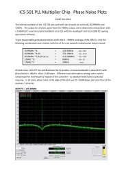
Version VCO /<br />
1 2 3 4 5 6 7 8 63<br />
Q2060 1990 995.0 663.3 497.5 398.0 331.7 284.3 248.8 31.6<br />
2240 1120.0 746.7 560.0 448.0 373.3 320.0 280.0 35.6<br />
Q2380 2200 1100.0 733.3 550.0 440.0 366.7 314.3 275.0 34.9<br />
2530 1265.0 843.3 632.5 506.0 421.7 361.4 316.3 40.2<br />
Q2690 2490 1245.0 830.0 622.5 498.0 415.0 355.7 311.3 39.5<br />
2865 1432.5 955.0 716.3 573.0 477.5 409.3 358.1 45.5<br />
Q3030 2810 1405.0 936.7 702.5 562.0 468.3 401.4 351.3 44.6<br />
3230 1615.0 1076.7 807.5 646.0 538.3 461.4 403.8 51.3<br />
Q3320 3130 1565.0 1043.3 782.5 626.0 521.7 447.1 391.3 49.7<br />
3600 1800.0 1200.0 900.0 720.0 600.0 514.3 450.0 57.1<br />
Q3740 3480 1740.0 1160.0 870.0 696.0 580.0 497.1 435.0 55.2<br />
4000 2000.0 1333.3 1000.0 800.0 666.7 571.4 500.0 63.5<br />
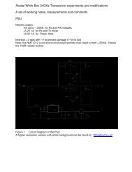
Circuit Operation<br />
The circuit diagram is shown in Figure 1. A higher resolution version of the circuit diagram is stored as<br />
lmx2541y.gif. The reference signal is ideally supplied from an external master oscillator or low phase noise<br />
clock generator. Reference input level is not critical, and the data sheets suggests -40dBm as a lower limit;<br />
the maximum should not exceed 3.3V peak. The 51Ω termination resistor, R3 can be increased if loading is<br />
too high for a TCXO. Use any value you feel comfortable with, or leave it out altogether<br />
The charge pump output is filtered in C1, C2 and R2 . Programmable on- chip components allow for up to a<br />
fourth order filter – see the data sheet for more details’<br />
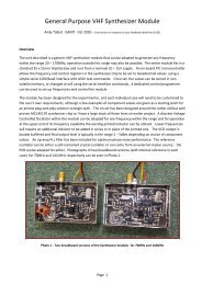
<strong>PCB</strong> Construction<br />
The <strong>PCB</strong> layout is shown in Figure 2, component references should tie-in with those in Figure 1. Component<br />
values not shown will depend on the design frequency and the PLL filter. Coupling and decoupling capacitors<br />
around the chip are 100nF – decoupling for high frequencies is internal to the chip Other decoupling ,<br />
including those for internal regulators should use the values shown.<br />
The only component that may give any difficulty in installation is the LM2541 itself. This should be fitted first,<br />
before any other components are added. The chip has 0.5mm pad spacing and is of the type where the<br />
connections are on the edge of the ceramic package, with no gull-wing tabs. The package is rectangular, with<br />
three pads each top and bottom, and nine on each side. A marker shows Pin 1 at the top left.<br />
This is how I solder the <strong>LMX2541</strong> device. Use a decent high magnification viewer; at least a headband type<br />
or for even greater magnification an old 50mm SLR camera lens is ideal. The pads on the <strong>PCB</strong> for the chip<br />
should first be tinned, aiming to keep an equal thickness of solder on each pad as shown in Photo 1. Then<br />
the pads should be liberally coated with flux. Double, triple and quadruple check k the IC alignment, place it<br />
central over the footprint so an equal amount of pad is showing on each side. Make sure there is flux still<br />
there on each pad. Press the IC down firmly, checking again for alignment. Peer though a magnifier at the IC<br />
pads sitting over the correct pads on the <strong>PCB</strong> while still pressing down on the IC. Look away for a few<br />
seconds to relax your eyes, return and check alignment again.<br />
Once absolutely certain each IC connection is above its pad, and unmoved, and still keeping it pressed down,<br />
using a medium-sized (typically 1mm) chisel-end soldering-iron bit place it in turn on each pad close to the IC,<br />
while watching the solder melt under the IC connections. The flux will cause a sort-of wicking action, drawing<br />
molten solder up from the pre-tinning to fill the gap to fix at least some of IC connections. Gently prod the<br />
chip to make sure it is now fixed by at least some pads and won’t move of its own accord. Now apply more<br />
flux to the IC / <strong>PCB</strong> and load the soldering iron tip with solder. Wipe the iron against each side of the chip in<br />
turn, gently pushing solder into the gaps. Providing there is enough flux present, it should nicely flow into the<br />
<strong>LMX2541</strong> <strong>Synthesizer</strong> Module <strong>G4JNT</strong> Page 2