ddr3 sdram - Spectrum Digital Support
ddr3 sdram - Spectrum Digital Support
ddr3 sdram - Spectrum Digital Support

Create successful ePaper yourself
Turn your PDF publications into a flip-book with our unique Google optimized e-Paper software.
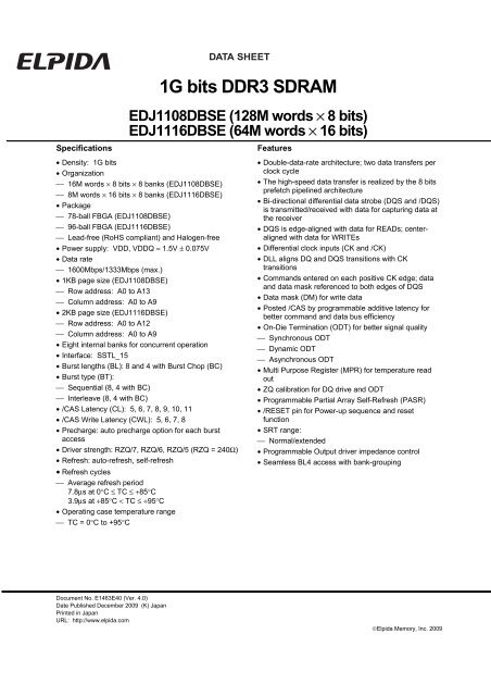
Specifications<br />
DATA SHEET<br />
1G bits DDR3 SDRAM<br />
EDJ1108DBSE (128M words × 8 bits)<br />
EDJ1116DBSE (64M words × 16 bits)<br />
• Density: 1G bits<br />
• Organization<br />
⎯ 16M words × 8 bits × 8 banks (EDJ1108DBSE)<br />
⎯ 8M words × 16 bits × 8 banks (EDJ1116DBSE)<br />
• Package<br />
⎯ 78-ball FBGA (EDJ1108DBSE)<br />
⎯ 96-ball FBGA (EDJ1116DBSE)<br />
⎯ Lead-free (RoHS compliant) and Halogen-free<br />
• Power supply: VDD, VDDQ = 1.5V ± 0.075V<br />
• Data rate<br />
⎯ 1600Mbps/1333Mbps (max.)<br />
• 1KB page size (EDJ1108DBSE)<br />
⎯ Row address: A0 to A13<br />
⎯ Column address: A0 to A9<br />
• 2KB page size (EDJ1116DBSE)<br />
⎯ Row address: A0 to A12<br />
⎯ Column address: A0 to A9<br />
• Eight internal banks for concurrent operation<br />
• Interface: SSTL_15<br />
• Burst lengths (BL): 8 and 4 with Burst Chop (BC)<br />
• Burst type (BT):<br />
⎯ Sequential (8, 4 with BC)<br />
⎯ Interleave (8, 4 with BC)<br />
• /CAS Latency (CL): 5, 6, 7, 8, 9, 10, 11<br />
• /CAS Write Latency (CWL): 5, 6, 7, 8<br />
• Precharge: auto precharge option for each burst<br />
access<br />
• Driver strength: RZQ/7, RZQ/6, RZQ/5 (RZQ = 240Ω)<br />
• Refresh: auto-refresh, self-refresh<br />
• Refresh cycles<br />
⎯ Average refresh period<br />
7.8µs at 0°C ≤ TC ≤ +85°C<br />
3.9µs at +85°C < TC ≤ +95°C<br />
• Operating case temperature range<br />
⎯ TC = 0°C to +95°C<br />
Features<br />
• Double-data-rate architecture; two data transfers per<br />
clock cycle<br />
• The high-speed data transfer is realized by the 8 bits<br />
prefetch pipelined architecture<br />
• Bi-directional differential data strobe (DQS and /DQS)<br />
is transmitted/received with data for capturing data at<br />
the receiver<br />
• DQS is edge-aligned with data for READs; centeraligned<br />
with data for WRITEs<br />
• Differential clock inputs (CK and /CK)<br />
• DLL aligns DQ and DQS transitions with CK<br />
transitions<br />
• Commands entered on each positive CK edge; data<br />
and data mask referenced to both edges of DQS<br />
• Data mask (DM) for write data<br />
• Posted /CAS by programmable additive latency for<br />
better command and data bus efficiency<br />
• On-Die Termination (ODT) for better signal quality<br />
⎯ Synchronous ODT<br />
⎯ Dynamic ODT<br />
⎯ Asynchronous ODT<br />
• Multi Purpose Register (MPR) for temperature read<br />
out<br />
• ZQ calibration for DQ drive and ODT<br />
• Programmable Partial Array Self-Refresh (PASR)<br />
• /RESET pin for Power-up sequence and reset<br />
function<br />
• SRT range:<br />
⎯ Normal/extended<br />
• Programmable Output driver impedance control<br />
• Seamless BL4 access with bank-grouping<br />
Document No. E1463E40 (Ver. 4.0)<br />
Date Published December 2009 (K) Japan<br />
Printed in Japan<br />
URL: http://www.elpida.com<br />
©Elpida Memory, Inc. 2009
EDJ1108DBSE, EDJ1116DBSE<br />
Ordering Information<br />
Part number<br />
EDJ1108DBSE-GN-F<br />
EDJ1108DBSE-DJ-F<br />
EDJ1116DBSE-GN-F<br />
EDJ1116DBSE-DJ-F<br />
Die<br />
revision<br />
Organization<br />
(words × bits)<br />
B 128M × 8 8<br />
64M × 16<br />
Internal<br />
banks<br />
JEDEC speed bin<br />
(CL-tRCD-tRP)<br />
DDR3-1600K (11-11-11)<br />
DDR3-1333H (9-9-9)<br />
DDR3-1600K (11-11-11)<br />
DDR3-1333H (9-9-9)<br />
Package<br />
78-ball FBGA<br />
96-ball FBGA<br />
Part Number<br />
E D J 11 08 D B SE - GN - F<br />
Elpida Memory<br />
Type<br />
D: Monolithic Device<br />
Product Family<br />
J: DDR3<br />
Density / Bank<br />
11: 1Gb / 8-bank<br />
Organization<br />
08: x8<br />
16: x16<br />
Environment code<br />
F: Lead Free (RoHS compliant)<br />
and Halogen Free<br />
Speed<br />
GN: DDR3-1600K (11-11-11)<br />
DJ: DDR3-1333H (9-9-9)<br />
Package<br />
SE: FBGA<br />
Power Supply, Interface<br />
D: 1.5V, SSTL_15 Die Rev.<br />
Data Sheet E1463E40 (Ver. 4.0)<br />
2
EDJ1108DBSE, EDJ1116DBSE<br />
Pin Configurations (×8 configuration)<br />
/xxx indicates active low signal.<br />
78-ball FBGA (×8 configuration)<br />
1<br />
2<br />
3<br />
7<br />
8<br />
9<br />
A<br />
B<br />
C<br />
D<br />
E<br />
F<br />
G<br />
H<br />
J<br />
K<br />
L<br />
M<br />
N<br />
VSS<br />
VSS<br />
VDDQ<br />
VSSQ<br />
VSS<br />
VSS<br />
VDD<br />
VSSQ<br />
DQ2<br />
DQ6<br />
VREFDQ VDDQ<br />
NC<br />
ODT<br />
NC<br />
VDD<br />
VSS<br />
VDD<br />
/CS<br />
BA0<br />
A7<br />
/RESET<br />
NC<br />
DQ0<br />
DQS<br />
/DQS<br />
DQ4<br />
/RAS<br />
/CAS<br />
/WE<br />
BA2<br />
A9<br />
A13<br />
NU/(/TDQS) VSS<br />
DM/TDQS VSSQ<br />
DQ1<br />
VDD<br />
DQ7<br />
CK<br />
/CK<br />
A10(AP)<br />
NC<br />
A11<br />
NC<br />
DQ3<br />
VSS<br />
DQ5<br />
VSS<br />
VDD<br />
ZQ<br />
VDDQ<br />
VSSQ<br />
VREFCA VSS<br />
A6<br />
A8<br />
VDD<br />
VSSQ<br />
VDDQ<br />
NC<br />
CKE<br />
NC<br />
VDD A3 A0 A12(/BC) BA1 VDD<br />
VSS A5 A2 A1 A4 VSS<br />
VDD<br />
VSS<br />
(Top view)<br />
Pin name Function Pin name Function<br />
A0 to A13* 3<br />
Address inputs<br />
A10 (AP): Auto precharge /RESET* 3<br />
Active low asynchronous reset<br />
A12(/BC): Burst chop<br />
BA0 to BA2* 3 Bank select VDD<br />
Supply voltage for internal<br />
circuit<br />
DQ0 to DQ7 Data input/output VSS Ground for internal circuit<br />
DQS, /DQS Differential data strobe VDDQ Supply voltage for DQ circuit<br />
TDQS, /TDQS Termination data strobe VSSQ Ground for DQ circuit<br />
/CS* 3 Chip select VREFDQ Reference voltage for DQ<br />
/RAS, /CAS, /WE* 3 Command input VREFCA Reference voltage<br />
CKE* 3 Clock enable ZQ<br />
Reference pin for ZQ<br />
calibration<br />
CK, /CK Differential clock input NC* 1 No connection<br />
DM Write data mask NU* 2 Not usable<br />
ODT* 3<br />
ODT control<br />
Notes: 1. Not internally connected with die.<br />
2. Don’t connect. Internally connected.<br />
3. Input only pins (address, command, CKE, ODT and /RESET) do not supply termination.<br />
Data Sheet E1463E40 (Ver. 4.0)<br />
3
EDJ1108DBSE, EDJ1116DBSE<br />
Pin Configurations (×16 configuration)<br />
/xxx indicates active low signal.<br />
96-ball FBGA<br />
1<br />
2<br />
3<br />
7<br />
8<br />
9<br />
A<br />
VDDQ<br />
DQU5<br />
DQU7<br />
DQU4<br />
VDDQ<br />
VSS<br />
B<br />
VSSQ<br />
VDD<br />
VSS<br />
/DQSU<br />
DQU6<br />
VSSQ<br />
C<br />
VDDQ<br />
DQU3<br />
DQU1<br />
DQSU<br />
DQU2<br />
VDDQ<br />
D<br />
VSSQ<br />
VDDQ<br />
DMU<br />
DQU0<br />
VSSQ<br />
VDD<br />
E<br />
VSS<br />
VSSQ<br />
DQL0<br />
DML<br />
VSSQ<br />
VDDQ<br />
F<br />
G<br />
H<br />
J<br />
K<br />
L<br />
M<br />
N<br />
P<br />
R<br />
T<br />
VDDQ DQL2 DQSL DQL1 DQL3 VSSQ<br />
VSSQ DQL6 /DQSL VDD VSS VSSQ<br />
VREFDQ VDDQ DQL4 DQL7 DQL5 VDDQ<br />
NC VSS /RAS CK VSS NC<br />
ODT VDD /CAS /CK VDD CKE<br />
NC /CS /WE A10(AP) ZQ NC<br />
VSS BA0 BA2 NC VREFCA VSS<br />
VDD A3 A0 A12(/BC) BA1 VDD<br />
VSS A5 A2 A1 A4 VSS<br />
VDD A7 A9 A11 A6 VDD<br />
VSS /RESET NC NC A8 VSS<br />
(Top view)<br />
Pin name Function Pin name Function<br />
A0 to A12* 2<br />
Address inputs<br />
A10(AP): Auto precharge<br />
/RESET* 2<br />
Active low asynchronous reset<br />
A12(/BC): Burst chop<br />
BA0 to BA2 Bank select VDD<br />
Supply voltage for internal<br />
circuit<br />
DQU0 to DQU7<br />
DQL0 to DQL7<br />
Data input/output VSS Ground for internal circuit<br />
DQSU, /DQSU<br />
DQSL, /DQSL<br />
Differential data strobe VDDQ Supply voltage for DQ circuit<br />
/CS* 2 Chip select VSSQ Ground for DQ circuit<br />
/RAS, /CAS, /WE* 2 Command input VREFDQ Reference voltage for DQ<br />
CKE* 2 Clock enable VREFCA Reference voltage<br />
CK, /CK Differential clock input ZQ<br />
Reference pin for ZQ<br />
calibration<br />
DMU, DML Write data mask NC* No connection<br />
ODT* 2<br />
ODT control<br />
Note: 1. Not internally connected with die.<br />
2. Input only pins (address, command, CKE, ODT and /RESET) do not supply termination.<br />
Data Sheet E1463E40 (Ver. 4.0)<br />
4
EDJ1108DBSE, EDJ1116DBSE<br />
CONTENTS<br />
Specifications.................................................................................................................................................1<br />
Features.........................................................................................................................................................1<br />
Ordering Information......................................................................................................................................2<br />
Part Number ..................................................................................................................................................2<br />
Pin Configurations (×8 configuration) ............................................................................................................3<br />
Pin Configurations (×16 configuration) ..........................................................................................................4<br />
Electrical Conditions ......................................................................................................................................7<br />
Absolute Maximum Ratings .......................................................................................................................... 7<br />
Operating Temperature Condition ................................................................................................................ 7<br />
Recommended DC Operating Conditions (TC = 0°C to +85°C, VDD, VDDQ = 1.5V ± 0.075V) ................... 8<br />
AC and DC Input Measurement Levels (TC = 0°C to +85°C, VDD, VDDQ = 1.5V ± 0.075V)....................... 8<br />
VREF Tolerances ......................................................................................................................................... 9<br />
Input Slew Rate Derating............................................................................................................................ 10<br />
AC and DC Logic Input Levels for Differential Signals................................................................................ 15<br />
AC and DC Output Measurement Levels (TC = 0°C to +85°C, VDD, VDDQ = 1.5V ± 0.075V) .................. 20<br />
AC Overshoot/Undershoot Specification..................................................................................................... 22<br />
Output Driver Impedance............................................................................................................................ 23<br />
On-Die Termination (ODT) Levels and I-V Characteristics .........................................................................25<br />
ODT Timing Definitions............................................................................................................................... 27<br />
IDD Measurement Conditions (TC = 0°C to +85°C, VDD, VDDQ = 1.5V ± 0.075V) ................................... 31<br />
Electrical Specifications...............................................................................................................................44<br />
DC Characteristics 1 (TC = 0°C to +85°C, VDD, VDDQ = 1.5V ± 0.075V) ................................................. 44<br />
DC Characteristics 2 (TC = 0°C to +85°C, VDD, VDDQ = 1.5V ± 0.075V) ................................................. 45<br />
Pin Capacitance (TC = 25°C, VDD, VDDQ = 1.5V ± 0.075V)..................................................................... 46<br />
Standard Speed Bins.................................................................................................................................. 47<br />
AC Characteristics (TC = 0°C to +85°C, VDD, VDDQ = 1.5V ± 0.075V, VSS, VSSQ = 0V)....................... 49<br />
Block Diagram .............................................................................................................................................57<br />
Pin Function.................................................................................................................................................58<br />
Command Operation ...................................................................................................................................60<br />
Command Truth Table................................................................................................................................ 60<br />
CKE Truth Table ......................................................................................................................................... 65<br />
Simplified State Diagram .............................................................................................................................66<br />
RESET and Initialization Procedure ............................................................................................................66<br />
Power-Up and Initialization Sequence ........................................................................................................ 66<br />
Reset and Initialization with Stable Power .................................................................................................. 67<br />
Programming the Mode Register.................................................................................................................68<br />
Mode Register Set Command Cycle Time (tMRD) .....................................................................................68<br />
MRS Command to Non-MRS Command Delay (tMOD) ............................................................................. 68<br />
DDR3 SDRAM Mode Register 0 [MR0] ...................................................................................................... 69<br />
Data Sheet E1463E40 (Ver. 4.0)<br />
5
EDJ1108DBSE, EDJ1116DBSE<br />
DDR3 SDRAM Mode Register 1 [MR1] ...................................................................................................... 70<br />
DDR3 SDRAM Mode Register 2 [MR2] ...................................................................................................... 71<br />
DDR3 SDRAM Mode Register 3 [MR3] ...................................................................................................... 72<br />
Burst Length (MR0) .................................................................................................................................... 73<br />
Burst Type (MR0) ....................................................................................................................................... 73<br />
DLL Enable (MR1) ...................................................................................................................................... 74<br />
DLL-off Mode .............................................................................................................................................. 74<br />
DLL on/off switching procedure .................................................................................................................. 75<br />
Additive Latency (MR1)............................................................................................................................... 77<br />
Write Leveling (MR1) .................................................................................................................................. 78<br />
TDQS, /TDQS function (MR1) .................................................................................................................... 81<br />
Extended Temperature Usage (MR2)......................................................................................................... 82<br />
Multi Purpose Register (MR3)..................................................................................................................... 84<br />
Operation of the DDR3 SDRAM..................................................................................................................92<br />
Read Timing Definition................................................................................................................................ 92<br />
Read Operation .......................................................................................................................................... 96<br />
Write Timing Definition.............................................................................................................................. 103<br />
Write Operation......................................................................................................................................... 104<br />
Write Timing Violations ............................................................................................................................. 110<br />
Write Data Mask ....................................................................................................................................... 111<br />
Precharge ................................................................................................................................................. 112<br />
Auto Precharge Operation ........................................................................................................................ 113<br />
Auto-Refresh............................................................................................................................................. 114<br />
Self-Refresh.............................................................................................................................................. 115<br />
Power-Down Mode ................................................................................................................................... 117<br />
Input Clock Frequency Change during Precharge Power-Down............................................................... 124<br />
On-Die Termination (ODT)........................................................................................................................ 125<br />
ZQ Calibration........................................................................................................................................... 137<br />
Addendum: Elpida DDR3 SDRAM Special Feature, Seamless BL4 Access with Bank-Grouping ...........139<br />
Background............................................................................................................................................... 139<br />
Solution..................................................................................................................................................... 141<br />
Seamless BL4 Access with Bank-Grouping Details.................................................................................. 144<br />
AC Specification Comparison Table for Bank-Grouping Feature Enabled/Disabled................................. 149<br />
Timing Diagram with Bank-Grouping Feature Enabled (MR3 bit A11 = 1)................................................ 151<br />
Package Drawing ......................................................................................................................................167<br />
78-ball FBGA ............................................................................................................................................ 167<br />
96-ball FBGA ............................................................................................................................................ 168<br />
Recommended Soldering Conditions........................................................................................................169<br />
Data Sheet E1463E40 (Ver. 4.0)<br />
6
EDJ1108DBSE, EDJ1116DBSE<br />
Electrical Conditions<br />
• All voltages are referenced to VSS (GND)<br />
• Execute power-up and Initialization sequence before proper device operation is achieved.<br />
Absolute Maximum Ratings<br />
Parameter Symbol Rating Unit Notes<br />
Power supply voltage VDD −0.4 to +1.975 V 1, 3<br />
Power supply voltage for output VDDQ −0.4 to +1.975 V 1, 3<br />
Input voltage VIN −0.4 to +1.975 V 1<br />
Output voltage VOUT −0.4 to +1.975 V 1<br />
Reference voltage VREFCA −0.4 to 0.6 × VDD V 3<br />
Reference voltage for DQ VREFDQ −0.4 to 0.6 × VDDQ V 3<br />
Storage temperature Tstg −55 to +100 °C 1, 2<br />
Power dissipation PD 1.0 W 1<br />
Short circuit output current IOUT 50 mA 1<br />
Notes: 1. Stresses greater than those listed under Absolute Maximum Ratings may cause permanent damage to<br />
the device. This is a stress rating only and functional operation of the device at these or any other<br />
conditions above those indicated in the operational sections of this specification is not implied. Exposure<br />
to absolute maximum rating conditions for extended periods may affect reliability.<br />
2. Storage temperature is the case surface temperature on the center/top side of the DRAM.<br />
3. VDD and VDDQ must be within 300mV of each other at all times; and VREF must be no greater than<br />
0.6 × VDDQ, When VDD and VDDQ are less than 500mV; VREF may be equal to or less than 300mV.<br />
Caution<br />
Exposing the device to stress above those listed in Absolute Maximum Ratings could cause<br />
permanent damage. The device is not meant to be operated under conditions outside the limits<br />
described in the operational section of this specification. Exposure to Absolute Maximum Rating<br />
conditions for extended periods may affect device reliability.<br />
Operating Temperature Condition<br />
Parameter Symbol Rating Unit Notes<br />
Operating case temperature TC 0 to +95 °C 1, 2, 3<br />
Notes: 1. Operating temperature is the case surface temperature on the center/top side of the DRAM.<br />
2. The Normal Temperature Range specifies the temperatures where all DRAM specifications will be<br />
supported. During operation, the DRAM case temperature must be maintained between 0°C to +85°C<br />
under all operating conditions.<br />
3. Some applications require operation of the DRAM in the Extended Temperature Range between +85°C<br />
and +95°C case temperature. Full specifications are guaranteed in this range, but the following additional<br />
conditions apply:<br />
a) Refresh commands must be doubled in frequency, therefore reducing the refresh interval tREFI to<br />
3.9µs. (This double refresh requirement may not apply for some devices.)<br />
b) If Self-refresh operation is required in the Extended Temperature Range, then it is mandatory to<br />
either use the Manual Self-Refresh mode with Extended Temperature Range capability (MR2 bit<br />
[A6, A7] = [0, 1]) or enable the optional Auto Self-Refresh mode (MR2 bit [A6, A7] = [1, 0]).<br />
Data Sheet E1463E40 (Ver. 4.0)<br />
7
EDJ1108DBSE, EDJ1116DBSE<br />
Recommended DC Operating Conditions (TC = 0°C to +85°C, VDD, VDDQ = 1.5V ± 0.075V)<br />
Parameter Symbol min. typ. max. Unit Notes<br />
Supply voltage VDD 1.425 1.5 1.575 V 1, 2<br />
Supply voltage for DQ VDDQ 1.425 1.5 1.575 V 1, 2<br />
Notes: 1. Under all conditions VDDQ must be less than or equal to VDD.<br />
2. VDDQ tracks with VDD. AC parameters are measured with VDD and VDDQ tied together.<br />
AC and DC Input Measurement Levels (TC = 0°C to +85°C, VDD, VDDQ = 1.5V ± 0.075V)<br />
Single-Ended AC and DC Input Levels for Command and Address<br />
Parameter Symbol min. typ. max. Unit Notes<br />
DC input logic high VIHCA (DC100) VREF + 0.100 ⎯ VDD V 1<br />
DC input logic low VILCA (DC100) VSS ⎯ VREF − 0.100 V 1<br />
AC input logic high VIHCA (AC175) VREF + 0.175 ⎯ ⎯* 2 V 1, 2<br />
AC input logic low VILCA (AC175) ⎯* 2 ⎯ VREF − 0.175 V 1, 2<br />
AC input logic high VIHCA (AC150) VREF + 0.150 ⎯ ⎯* 2 V 1, 2<br />
AC input logic low VILCA (AC150) ⎯* 2 ⎯ VREF − 0.150 V 1, 2<br />
Input reference voltage<br />
for address, command VREFCA (DC) 0.49 × VDD ⎯ 0.51 × VDD V 3, 4<br />
inputs<br />
Notes: 1. For input only pins except /RESET; VREF = VREFCA (DC).<br />
2. See Overshoot and Undershoot Specifications section.<br />
3. The AC peak noise on VREF may not allow VREF to deviate from VREFCA (DC) by more than ±1% VDD<br />
(for reference: approx. ±15 mV).<br />
4. For reference: approx. VDD/2 ± 15 mV.<br />
Single-Ended AC and DC Input Levels for DQ and DM<br />
Parameter Symbol min. typ. max. Unit Notes<br />
DC input logic high VIHDQ (DC100) VREF + 0.100 ⎯ VDD V 1<br />
DC input logic low VILDQ (DC100) VSS ⎯ VREF − 0.100 V 1<br />
AC input logic high VIHDQ (AC175) ⎯ ⎯ ⎯ V 1, 2<br />
AC input logic high VIHDQ (AC150) VREF + 0.150 ⎯ ⎯* 2 1, 2<br />
AC input logic low VILDQ (AC175) ⎯ ⎯ ⎯ V 1, 2<br />
AC input logic low VILDQ (AC150) ⎯* 2 ⎯ VREF − 0.150 1, 2<br />
Input reference<br />
voltage for DQ, DM VREFDQ (DC) 0.49 × VDD ⎯ 0.51 × VDD V 3, 4<br />
inputs<br />
Notes: 1. For DQ and DM: VREF = VREFDQ (DC).<br />
2. See Overshoot and Undershoot Specifications section.<br />
3. The AC peak noise on VREF may not allow VREF to deviate from VREFDQ (DC) by more than ±1% VDD<br />
(for reference: approx. ±15 mV).<br />
4. For reference: approx. VDD/2 ± 15 mV.<br />
Data Sheet E1463E40 (Ver. 4.0)<br />
8
EDJ1108DBSE, EDJ1116DBSE<br />
VREF Tolerances<br />
The dc-tolerance limits and ac-noise limits for the reference voltages VREFCA and VREFDQ are shown in Figure<br />
VREF(DC) Tolerance and VREF AC-Noise Limits. It shows a valid reference voltage VREF(t) as a function of time.<br />
(VREF stands for VREFCA and VREFDQ likewise).<br />
VREF(DC) is the linear average of VREF(t) over a very long period of time (e.g. 1 sec). This average has to meet the<br />
min/max requirements in the table of(Single-Ended AC and DC Input Levels for Command and Address).<br />
Furthermore VREF(t) may temporarily deviate from VREF(DC) by no more than +/- 1% VDD.<br />
voltage<br />
VDD<br />
VREF AC-noise<br />
VREF(t)<br />
VREF(DC)<br />
VREF(DC)max.<br />
VDD/2<br />
VREF(DC)min.<br />
VSS<br />
VREF(DC) Tolerance and VREF AC-Noise Limits<br />
time<br />
The voltage levels for setup and hold time measurements VIH(AC), VIH(DC), VIL(AC) and VIL(DC) are dependent<br />
on VREF.<br />
VREF shall be understood as VREF(DC), as defined in figure above, VREF(DC) Tolerance and VREF AC-Noise<br />
Limits.<br />
This clarifies that DC-variations of VREF affect the absolute voltage a signal has to reach to achieve a valid high or<br />
low level and therefore the time to which setup and hold is measured. System timing and voltage budgets need to<br />
account for VREF(DC) deviations from the optimum position within the data-eye of the input signals.<br />
This also clarifies that the DRAM setup/hold specification and derating values need to include time and voltage<br />
associated with VREF AC-noise. Timing and voltage effects due to ac-noise on VREF up to the specified limit (±1%<br />
of VDD) are included in DRAM timings and their associated deratings.<br />
Data Sheet E1463E40 (Ver. 4.0)<br />
9
EDJ1108DBSE, EDJ1116DBSE<br />
Input Slew Rate Derating<br />
For all input signals the total tIS, tDS (setup time) and tIH, tDH (hold time) required is calculated by adding the data<br />
sheet tIS (base), tDS (base) and tIH (base), tDH (base) value to the ∆tIS, ∆tDS and ∆tIH, ∆tDH derating value<br />
respectively.<br />
Example: tDS (total setup time) = tDS (base) + ∆tDS.<br />
Setup (tIS, tDS) nominal slew rate for a rising signal is defined as the slew rate between the last crossing of VREF<br />
(DC) and the first crossing of VIH (AC) min. Setup (tIS, tDS) nominal slew rate for a falling signal is defined as the<br />
slew rate between the last crossing of VREF (DC) and the first crossing of VIL (AC) max. If the actual signal is<br />
always earlier than the nominal slew rate line between shaded ‘VREF (DC) to AC region’, use nominal slew rate for<br />
derating value (See the figure of Slew Rate Definition Nominal).<br />
If the actual signal is later than the nominal slew rate line anywhere between shaded ‘VREF (DC) to AC region’, the<br />
slew rate of a tangent line to the actual signal from the AC level to DC level is used for derating value (see the figure<br />
of Slew Rate Definition Tangent).<br />
Hold (tIH, tDH) nominal slew rate for a rising signal is defined as the slew rate between the last crossing of<br />
VIL (DC) max. and the first crossing of VREF (DC). Hold (tIH, tDH) nominal slew rate for a falling signal is defined<br />
as the slew rate between the last crossing of VIH (DC) min. and the first crossing of VREF (DC). If the actual signal<br />
is always later than the nominal slew rate line between shaded ‘DC level to VREF (DC) region’, use nominal slew<br />
rate for derating value (See the figure of Slew Rate Definition Nominal).<br />
If the actual signal is earlier than the nominal slew rate line anywhere between shaded ‘DC to VREF (DC) region’,<br />
the slew rate of a tangent line to the actual signal from the DC level to VREF (DC) level is used for derating value<br />
(see the figure of Slew Rate Definition Tangent).<br />
For a valid transition the input signal has to remain above/below VIH/VIL(AC) for some time tVAC (see the table of<br />
Required time tVAC above VIH(AC) {below VIL(AC)} for valid transition).<br />
Although for slow slew rates the total setup time might be negative (i.e. a valid input signal will not have reached<br />
VIH/IL (AC) at the time of the rising clock transition) a valid input signal is still required to complete the transition and<br />
reach VIH/IL (AC).<br />
For slew rates in between the values listed in the tables below, the derating values may obtained by linear<br />
interpolation.<br />
These values are typically not subject to production test. They are verified by design and characterization.<br />
[Address/Command Setup and Hold Base-Values for 1V/ns]<br />
DDR3-1333 DDR3-1600 Unit Reference<br />
tIS(base) AC175 65 45 ps VIH/VIL(AC)<br />
tIH(base) DC100 140 120 ps VIH/VIL(DC)<br />
tIS(base) AC150 65 + 125 45 + 125 ps VIH/VIL(AC)<br />
Notes: 1 AC/DC referenced for 1V/ns Address/Command slew rate and 2V/ns differential CK, /CK slew rate.<br />
2. The tHS (base) AC150 specifications are adjusted from the tIS(base) specification by adding an additional<br />
100ps of derating to accommodate for the lower alternate threshold of 150mV and another 25ps to<br />
account for the earlier reference point [(175mv − 150mv)/1V/ns]<br />
Data Sheet E1463E40 (Ver. 4.0)<br />
10
EDJ1108DBSE, EDJ1116DBSE<br />
[Derating Values of tIS/tIH AC/DC based AC175 Threshold (DDR3-1333, 1600)]<br />
CMD,<br />
ADD<br />
slew<br />
rate<br />
(V/ns)<br />
∆tIS, ∆tIH derating in [ps] AC/DC based<br />
AC175 Threshold -> VIH(AC)=VREF(DC)+175mV, VIL(AC)=VREF(DC)-175mV<br />
CK, /CK differential slew rate<br />
4.0 V/ns 3.0 V/ns 2.0 V/ns 1.8 V/ns 1.6 V/ns 1.4 V/ns 1.2 V/ns 1.0 V/ns<br />
∆tIS ∆tIH ∆tIS ∆tIH ∆tIS ∆tIH ∆tIS ∆tIH ∆tIS ∆tIH ∆tIS ∆tIH ∆tIS ∆tIH ∆tIS ∆tIH Unit<br />
2.0 +88 +50 +88 +50 +88 +50 +96 +58 +104 +66 +112 +74 +120 +84 +128 +100 ps<br />
1.5 +59 +34 +59 +34 +59 +34 +67 +42 +75 +50 +83 +58 +91 +68 +99 +84 ps<br />
1.0 0 0 0 0 0 0 +8 +8 +16 +16 +24 +24 +32 +34 +40 +50 ps<br />
0.9 −2 −4 −2 −4 −2 −4 +6 +4 +14 +12 +22 +20 +30 +30 +38 +46 ps<br />
0.8 −6 −10 −6 −10 −6 −10 +2 −2 +10 +6 +18 +14 +26 +24 +34 +40 ps<br />
0.7 −11 −16 −11 −16 −11 −16 −3 −8 +5 0 +13 +8 +21 +18 +29 +34 ps<br />
0.6 −17 −26 −17 −26 −17 −26 −9 −18 −1 −10 +7 −2 +15 +8 +23 +24 ps<br />
0.5 −35 −40 −35 −40 −35 −40 −27 −32 −19 −24 −11 −16 −2 −6 +5 +10 ps<br />
0.4 −62 −60 −62 −60 −62 −60 −54 −52 −46 −44 −38 −36 −30 −26 −22 −10 ps<br />
[Derating Values of tIS/tIH AC/DC based-Alternate AC150 Threshold (DDR3-1333, 1600)]<br />
∆tIS, ∆tIH derating in [ps] AC/DC based<br />
Alternate AC150 Threshold -> VIH(AC)=VREF(DC)+150mV, VIL(AC)=VREF(DC)-150mV<br />
CMD,<br />
ADD<br />
slew<br />
rate<br />
(V/ns)<br />
CK, /CK differential slew rate<br />
4.0 V/ns 3.0 V/ns 2.0 V/ns 1.8 V/ns 1.6 V/ns 1.4 V/ns 1.2 V/ns 1.0 V/ns<br />
∆tIS ∆tIH ∆tIS ∆tIH ∆tIS ∆tIH ∆tIS ∆tIH ∆tIS ∆tIH ∆tIS ∆tIH ∆tIS ∆tIH ∆tIS ∆tIH Unit<br />
2.0 +75 +50 +75 +50 +75 +50 +83 +58 +91 +66 +99 +74 +107 +84 +115 +100 ps<br />
1.5 +50 +34 +50 +34 +50 +34 +58 +42 +66 +50 +74 +58 +82 +68 +90 +84 ps<br />
1.0 0 0 0 0 0 0 +8 +8 +16 +16 +24 +24 +32 +34 +40 +50 ps<br />
0.9 0 −4 0 −4 0 −4 +8 +4 +16 +12 +24 +20 +32 +30 +40 +46 ps<br />
0.8 0 −10 0 −10 0 −10 +8 −2 +16 +6 +24 +14 +32 +24 +40 +40 ps<br />
0.7 0 −16 0 −16 0 −16 +8 −8 +16 0 +24 +8 +32 +18 +40 +34 ps<br />
0.6 −1 −26 −1 −26 −1 −26 +7 −18 +15 −10 +23 −2 +31 +8 +39 +24 ps<br />
0.5 −10 −40 −10 −40 −10 −40 −2 −32 +6 −24 +14 −16 +22 −6 +30 +10 ps<br />
0.4 −25 −60 −25 −60 −25 −60 −17 −52 −9 −44 −1 −36 +7 −26 +15 −10 ps<br />
[Required time tVAC above VIH(AC) {below VIL(AC)} for Valid Transition]<br />
tVAC @ AC175 [ps]<br />
tVAC @ AC150 [ps]<br />
Slew rate (V/ns) min. max. min. max.<br />
>2.0 75 ⎯ 175 ⎯<br />
2.0 57 ⎯ 170 ⎯<br />
1.5 50 ⎯ 167 ⎯<br />
1.0 38 ⎯ 163 ⎯<br />
0.9 34 ⎯ 162 ⎯<br />
0.8 29 ⎯ 161 ⎯<br />
0.7 22 ⎯ 159 ⎯<br />
0.6 13 ⎯ 155 ⎯<br />
0.5 0 ⎯ 150 ⎯<br />
EDJ1108DBSE, EDJ1116DBSE<br />
[Data Setup and Hold Base-Values]<br />
DDR3-1333 DDR3-1600 Unit Reference<br />
tDS(base) AC175 ⎯ ⎯ ps VIH/VIL(AC)<br />
tDS(base) AC150 30 10 ps VIH/VIL(AC)<br />
tDH(base) DC100 65 45 ps VIH/VIL(DC)<br />
Note: 1 AC/DC referenced for 1V/ns DQ slew rate and 2V/ns DQS slew rate<br />
[Derating Values of tDS/tDH AC/DC based, AC150 (DDR3-1333, 1600)]<br />
∆tDS, ∆tDH derating in [ps] AC/DC based<br />
DQS, /DQS differential slew rate<br />
4.0 V/ns 3.0 V/ns 2.0 V/ns 1.8 V/ns 1.6 V/ns 1.4 V/ns 1.2 V/ns 1.0 V/ns<br />
∆tDS ∆tDH ∆tDS ∆tDH ∆tDS ∆tDH ∆tDS ∆tDH ∆tDS ∆tDH ∆tDS ∆tDH ∆tDS ∆tDH ∆tDS ∆tDH Unit<br />
2.0 +75 +50 +75 +50 +75 +50 ⎯ ⎯ ⎯ ⎯ ⎯ ⎯ ⎯ ⎯ ⎯ ⎯ ps<br />
1.5 +50 +34 +50 +34 +50 +34 +58 +42 ⎯ ⎯ ⎯ ⎯ ⎯ ⎯ ⎯ ⎯ ps<br />
1.0 0 0 0 0 0 0 +8 +8 +16 +16 ⎯ ⎯ ⎯ ⎯ ⎯ ⎯ ps<br />
DQ 0.9 ⎯ ⎯ 0 −4 0 −4 +8 +4 +16 +12 +24 +20 ⎯ ⎯ ⎯ ⎯ ps<br />
slew<br />
rate 0.8 ⎯ ⎯ ⎯ ⎯ 0 −10 +8 −2 +16 +6 +24 +14 +32 +24 ⎯ ⎯ ps<br />
(V/ns) 0.7 ⎯ ⎯ ⎯ ⎯ ⎯ ⎯ +8 −8 +16 0 +24 +8 +32 +18 +40 +34 ps<br />
0.6 ⎯ ⎯ ⎯ ⎯ ⎯ ⎯ ⎯ ⎯ +15 −10 +23 −2 +31 +8 +39 +24 ps<br />
0.5 ⎯ ⎯ ⎯ ⎯ ⎯ ⎯ ⎯ ⎯ ⎯ ⎯ +14 −16 +22 −6 +30 +10 ps<br />
0.4 ⎯ ⎯ ⎯ ⎯ ⎯ ⎯ ⎯ ⎯ ⎯ ⎯ ⎯ ⎯ +7 −26 +15 −10 ps<br />
[Required time tVAC above VIH(AC) {below VIL(AC)} for valid transition]<br />
DDR3-1333, 1600 (AC150)<br />
tVAC [ps]<br />
Slew rate (V/ns) min. max.<br />
>2.0 175 ⎯<br />
2.0 170 ⎯<br />
1.5 167 ⎯<br />
1.0 163 ⎯<br />
0.9 162 ⎯<br />
0.8 161 ⎯<br />
0.7 159 ⎯<br />
0.6 155 ⎯<br />
0.5 150 ⎯<br />
EDJ1108DBSE, EDJ1116DBSE<br />
CK<br />
/CK<br />
tIS tIH tIS tIH<br />
VDD<br />
VIH (AC) min.<br />
VIH (DC) min.<br />
VREF (DC)<br />
VIL (DC) max.<br />
VREF to AC<br />
region<br />
DC to VREF<br />
region<br />
nominal<br />
slew rate<br />
tVAC<br />
nominal<br />
slew rate<br />
DC to VREF<br />
region<br />
VIL (AC) max.<br />
VREF to AC<br />
region<br />
VSS<br />
tVAC<br />
∆TFS ∆TRH ∆TRS<br />
∆TFH<br />
Slew Rate Definition Nominal (CK, /CK)<br />
/DQS<br />
DQS<br />
VDD<br />
VIH (AC) min.<br />
VREF to AC<br />
region<br />
tDS tDH tDS tDH<br />
tVAC<br />
VIH (DC) min.<br />
VREF (DC)<br />
VIL (DC) max.<br />
DC to VREF<br />
region<br />
nominal<br />
slew rate<br />
nominal<br />
slew rate<br />
DC to VREF<br />
region<br />
VIL (AC) max.<br />
VREF to AC<br />
region<br />
VSS<br />
tVAC<br />
∆TFS ∆TRH ∆TRS<br />
∆TFH<br />
Slew Rate Definition Nominal (DQS, /DQS)<br />
Setup slew rate<br />
Falling signal<br />
=<br />
VREF (DC) - VIL (AC) max.<br />
∆TFS<br />
Setup slew rate<br />
Rising signal<br />
=<br />
VIH (AC) min. - VREF (DC)<br />
∆TRS<br />
Hold slew rate<br />
Rising signal<br />
=<br />
VREF (DC) - VIL (DC) max.<br />
∆TRH<br />
Hold slew rate<br />
Falling signal<br />
VIH (DC) min. - VREF (DC)<br />
=<br />
∆TFH<br />
Data Sheet E1463E40 (Ver. 4.0)<br />
13
EDJ1108DBSE, EDJ1116DBSE<br />
CK<br />
/CK<br />
VDD<br />
VIH (AC) min.<br />
tIS tIH tIS tIH<br />
tVAC<br />
VIH (DC) min.<br />
VREF (DC)<br />
VREF to AC<br />
region<br />
DC to VREF<br />
region<br />
tangent<br />
line<br />
nominal<br />
line<br />
tangent<br />
line<br />
nominal<br />
line<br />
VIL (DC) max.<br />
nominal<br />
line<br />
DC to VREF<br />
region<br />
nominal<br />
line<br />
VIL (AC) max.<br />
VREF to AC<br />
region<br />
VSS<br />
tVAC<br />
∆TFS ∆TRH ∆TRS<br />
∆TFH<br />
Slew Rate Definition Tangent (CK, /CK)<br />
/DQS<br />
DQS<br />
VDD<br />
VIH (AC) min.<br />
tDS tDH tDS tDH<br />
tVAC<br />
VIH (DC) min.<br />
VREF (DC)<br />
VREF to AC<br />
region<br />
DC to VREF<br />
region<br />
tangent<br />
line<br />
nominal<br />
line<br />
tangent<br />
line<br />
nominal<br />
line<br />
VIL (DC) max.<br />
nominal<br />
line<br />
DC to VREF<br />
region<br />
nominal<br />
line<br />
VIL (AC) max.<br />
VREF to AC<br />
region<br />
VSS<br />
tVAC<br />
∆TFS ∆TRH ∆TRS<br />
∆TFH<br />
Slew Rate Definition Tangent (DQS, /DQS)<br />
Setup slew rate<br />
Falling signal<br />
=<br />
tangent line [VREF (DC) - VIL (AC) max.]<br />
∆TFS<br />
Setup slew rate<br />
Rising signal<br />
=<br />
tangent line [VIH (AC) min. - VREF (DC)]<br />
∆TRS<br />
Hold slew rate<br />
Rising signal<br />
=<br />
tangent line [VREF (DC) - VIL (DC) max.]<br />
∆TRH<br />
Hold slew rate<br />
Falling signal<br />
=<br />
tangent line [VIH (DC) min. - VREF (DC)]<br />
∆TFH<br />
Data Sheet E1463E40 (Ver. 4.0)<br />
14
EDJ1108DBSE, EDJ1116DBSE<br />
AC and DC Logic Input Levels for Differential Signals<br />
Differential signal definition<br />
tDVAC<br />
Differential Input Voltage (i.e. DQS - /DQS, CK - /CK)<br />
VIH.DIFF.AC.min.<br />
VIH.DIFF.min.<br />
0<br />
VIL.DIFF.max.<br />
VIL.DIFF.AC.max.<br />
half cycle<br />
tDVAC<br />
time<br />
Definition of Differential AC-swing and “time above AC-level” tDVAC<br />
[Differential AC and DC Input Levels]<br />
Parameter Symbol min. typ. max. Unit Notes<br />
Differential input logic high VIHdiff +0.200 ⎯ ⎯* 3 V 1<br />
Differential input logic low VILdiff ⎯* 3 ⎯ –0.200 V 1<br />
Differential input logic AC<br />
2 × (VIH (AC) − ⎯<br />
VIHdiff (AC)<br />
VREF)<br />
⎯* 3 V 2<br />
Differential input logic AC VILdiff (AC) ⎯* 3 ⎯ 2 × (VIL(AC) − VREF) V 2<br />
Notes: 1 Used to define a differential signal slew-rate.<br />
2. For CK, /CK use VIH/VIL(AC) of address/command and VREFCA; for strobes (DQS, /DQS, DQSL,<br />
/DQSL, DQSU, /DQSU) use VIH/VIL(AC) of DQs and VREFDQ; if a reduced ac-high or ac-low level is<br />
used for a signal group, then the reduced level applies also here.<br />
3 These values are not defined, however the single ended components of differential signal CK, /CK, DQS,<br />
/DQS, DQSL, /DQSL, DQSU, /DQSU need to be within the respective limits (VIH(DC) max, VIL(DC)min)<br />
for single-ended signals as well as the limitations for overshoot and undershoot. Refer to Overshoot and<br />
Undershoot specifications.<br />
Data Sheet E1463E40 (Ver. 4.0)<br />
15
EDJ1108DBSE, EDJ1116DBSE<br />
[Required time tVAC above VIH(AC) {below VIL(AC)} for valid transition]<br />
@[VIH/Ldiff (AC)] = 350 mV<br />
@[VIH/Ldiff (AC)] = 300 mV<br />
tDVAC [ps]<br />
tDVAC [ps]<br />
Slew rate (V/ns) min. max. min. max.<br />
>4.0 75 ⎯ 175 ⎯<br />
4.0 57 ⎯ 170 ⎯<br />
3.0 50 ⎯ 167 ⎯<br />
2.0 38 ⎯ 163 ⎯<br />
1.8 34 ⎯ 162 ⎯<br />
1.6 29 ⎯ 161 ⎯<br />
1.4 22 ⎯ 159 ⎯<br />
1.2 13 ⎯ 155 ⎯<br />
1.0 0 ⎯ 150 ⎯<br />
EDJ1108DBSE, EDJ1116DBSE<br />
Single-Ended Requirements for Differential Signals<br />
Each individual component of a differential signal (CK, DQS, DQSL, DQSU, /CK, /DQS, /DQSL or /DQSU) has also<br />
to comply with certain requirements for single-ended signals.<br />
CK and /CK have to approximately reach VSEH min. / VSEL max. (approximately equal to the AC-levels (VIH(AC) /<br />
VIL(AC)) for Address/command signals) in every half-cycle.<br />
DQS, DQSL, DQSU, /DQS, /DQSL have to reach VSEH min./VSEL max. (approximately the AC-levels (VIH(AC) /<br />
VIL(AC)) for DQ signals) in every half-cycle preceding and following a valid transition.<br />
Note that the applicable ac-levels for Address/command and DQ’s might be different per speed-bin etc. E.g. if VIH<br />
150 (AC)/VIL 150 (AC) is used for Address/command signals, then these ac-levels apply also for the single ended<br />
components of differential CK and /CK.<br />
VDD or VDDQ<br />
VSEH min.<br />
VSEH<br />
VDD/2 or VDDQ/2<br />
VSEL max.<br />
CK or DQS<br />
VSS or VSSQ<br />
Single-Ended Requirement for Differential Signals.<br />
VSEL<br />
time<br />
Note that while Address/command and DQ signal requirements are with respect to VREF, the single-ended<br />
components of differential signals have a requirement with respect to VDD / 2; this is nominally the same. The<br />
transition of single-ended signals through the ac-levels is used to measure setup time. For single-ended components<br />
of differential signals the requirement to reach VSEL max, VSEH min has no bearing on timing, but adds a restriction<br />
on the common mode characteristics of these signals.<br />
Data Sheet E1463E40 (Ver. 4.0)<br />
17
EDJ1108DBSE, EDJ1116DBSE<br />
[Single-ended levels for CK, DQS, DQSL, DQSU, /CK, /DQS, /DQSL or /DQSU]<br />
Parameter Symbol min. typ. max. Unit Notes<br />
Single-ended high level for strobes (VDD/2) + 0.175 ⎯ ⎯* 3 V 1, 2<br />
VSEH<br />
Single-ended high level for CK, /CK<br />
(VDD/2) + 0.175 ⎯ ⎯* 3 V 1, 2<br />
Single-ended low level for strobes ⎯* 3 ⎯ (VDD/2) − 0.175 V 1, 2<br />
VSEL<br />
Single-ended low level for CK, /CK<br />
⎯* 3 ⎯ (VDD/2) − 0.175 V 1, 2<br />
Notes: 1. For CK, /CK use VIH/VIL(AC) of ADD/CMD; for strobes (DQS, /DQS, DQSL, /DQSL, DQSU, /DQSU) use<br />
VIH/VIL(AC) of DQs.<br />
2. VIH(AC)/VIL(AC) for DQs is based on VREFDQ; VIH(AC)/VIL(AC) for address/command is based on<br />
VREFCA; if a reduced ac-high or ac-low level is used for a signal group, then the reduced level applies<br />
also here.<br />
3 These values are not defined, however the single ended components of differential signals CK, /CK, DQS,<br />
/DQS, DQSL, /DQSL, DQSU, /DQSU need to be within the respective limits (VIH(DC) max, VIL(DC)min)<br />
for single-ended signals as well as the limitations for overshoot and undershoot. Refer to Overshoot and<br />
Undershoot specifications.<br />
To guarantee tight setup and hold times as well as output skew parameters with respect to clock and strobe, each<br />
cross point voltage of differential input signals (CK, /CK and DQS, /DQS) must meet the requirements in table above.<br />
The differential input cross point voltage VIX is measured from the actual cross point of true and complement signal<br />
to the midlevel between of VDD and VSS.<br />
VDD<br />
CK, DQS<br />
VDD/2<br />
VIX<br />
VIX<br />
VIX<br />
/CK, /DQS<br />
VSS<br />
VIX Definition<br />
[Cross point voltage for differential input signals (CK, DQS)]<br />
Parameter Symbol pins min. max. Unit Note<br />
Differential input cross point voltage<br />
relative to VDD/2<br />
VIX CK, /CK −150 150 mV<br />
−175 175 mV 1<br />
VIX DQS, /DQS −150 150 mV<br />
Note: 1. Extended range for VIX is only allowed for clock and if CK and /CK are monotonic, have a single-ended<br />
swing VSEL/VSEH of at least VDD/2 +/-250 mV, and the differential slew rate of CK - /CK is larger than 3<br />
V/ ns. Refer to the table of Cross point voltage for differential input signals (CK, DQS) for VSEL and VSEH<br />
standard values.<br />
Data Sheet E1463E40 (Ver. 4.0)<br />
18
EDJ1108DBSE, EDJ1116DBSE<br />
[Differential Input Slew Rate Definition]<br />
Measured<br />
Description From To Defined by Applicable for Note<br />
Differential input slew rate<br />
for rising edge<br />
(CK - /CK and DQS - /DQS)<br />
Differential input slew rate<br />
for falling edge<br />
(CK - /CK and DQS - /DQS)<br />
VILdiff (max.)<br />
VIHdiff (min.)<br />
VIHdiff (min.)<br />
VILdiff (max.)<br />
VIHdiff (min.) – VILdiff (max.)<br />
∆TRdiff<br />
VIHdiff (min.) – VILdiff (max.)<br />
∆TFdiff<br />
Note: The differential signal (i.e. CK, /CK and DQS, /DQS) must be linear between these thresholds.<br />
VIHdiff(min.)<br />
0<br />
VILdiff (max.)<br />
∆TFdiff<br />
∆TRdiff<br />
VIHdiff (min.) − VILdiff (max.)<br />
VIHdiff (min.) − VILdiff (max.)<br />
Falling slew =<br />
Rising slew =<br />
∆TFdiff<br />
∆TRdiff<br />
Differential Input Slew Rate Definition for DQS, /DQS and CK, /CK<br />
Data Sheet E1463E40 (Ver. 4.0)<br />
19
EDJ1108DBSE, EDJ1116DBSE<br />
AC and DC Output Measurement Levels (TC = 0°C to +85°C, VDD, VDDQ = 1.5V ± 0.075V)<br />
Parameter Symbol Specification Unit Notes<br />
DC output high measurement level<br />
(for IV curve linearity)<br />
VOH (DC) 0.8 × VDDQ V<br />
DC output middle measurement level<br />
(for IV curve linearity)<br />
VOM (DC) 0.5 × VDDQ V<br />
DC output low measurement level<br />
(for IV curve linearity)<br />
VOL (DC) 0.2 × VDDQ V<br />
AC output high measurement level<br />
(for output slew rate)<br />
VOH (AC) VTT + 0.1 × VDDQ V 1<br />
AC output low measurement level<br />
(for output slew rate)<br />
VOL (AC) VTT − 0.1 × VDDQ V 1<br />
AC differential output high measurement<br />
VOHdiff<br />
level (for output slew rate)<br />
0.2 × VDDQ V 2<br />
AC differential output low measurement<br />
level (for output slew rate)<br />
VOLdiff −0.2 × VDDQ V 2<br />
AC differential cross point voltage VOX (AC) TBD mV<br />
Notes: 1. The swing of ±0.1 × VDDQ is based on approximately 50% of the static single-ended output high or low<br />
swing with a driver impedance of 34Ω and an effective test load of 25Ω to VTT = VDDQ/2 at each of the<br />
differential outputs.<br />
2. The swing of ±0.2 × VDDQ is based on approximately 50% of the static single-ended output high or low<br />
swing with a driver impedance of 34Ω and an effective test load of 25Ω to VTT = VDDQ/2 at each of the<br />
differential outputs.<br />
Output Slew Rate Definitions<br />
[Single-Ended Output Slew Rate Definition]<br />
Measured<br />
Description From To Defined by<br />
Output slew rate for rising edge VOL (AC) VOH (AC)<br />
Output slew rate for falling edge VOH (AC) VOL (AC)<br />
VOH (AC) – VOL (AC)<br />
∆TRse<br />
VOH (AC) – VOL (AC)<br />
∆TFse<br />
VOH (AC)<br />
VTT<br />
VOL (AC)<br />
∆TFse<br />
∆TRse<br />
Falling slew =<br />
VOH (AC) − VOL (AC)<br />
∆TFse<br />
Rising slew =<br />
VOH (AC) − VOL (AC)<br />
∆TRse<br />
Input Slew Rate Definition for Single-Ended Signals<br />
Data Sheet E1463E40 (Ver. 4.0)<br />
20
EDJ1108DBSE, EDJ1116DBSE<br />
[Differential Output Slew Rate Definition]<br />
Measured<br />
Description From To Defined by<br />
Differential output slew rate<br />
for rising edge<br />
VOLdiff (AC)<br />
VOHdiff (AC)<br />
VOHdiff(AC) – VOLdiff (AC)<br />
∆TRdiff<br />
Differential output slew rate<br />
for falling edge<br />
VOHdiff (AC)<br />
VOLdiff (AC)<br />
VOHdiff (AC) – VOLdiff (AC)<br />
∆TFdiff<br />
VOHdiff (AC)<br />
0<br />
VOLdiff (AC)<br />
∆TFdiff<br />
∆TRdiff<br />
VOHdiff (AC) − VOLdiff (AC)<br />
VOHdiff (AC) − VOLdiff (AC)<br />
Falling slew =<br />
Rising slew =<br />
∆TFdiff<br />
∆TRdiff<br />
Differential Input Slew Rate Definition for DQS, /DQS and CK, /CK<br />
Output Slew Rate (RON = RZQ/7 setting)<br />
Parameter Symbol Speed min. max. Unit Notes<br />
Output slew rate<br />
(Single-ended)<br />
Output slew rate<br />
(Differential)<br />
SRQse<br />
SRQdiff<br />
DDR3-1333<br />
DDR3-1600<br />
DDR3-1333<br />
DDR3-1600<br />
2.5 5 V/ns 1<br />
5 10 V/ns 1<br />
Remark: SR = slew rate. se = single-ended signals. diff = differential signals. Q = Query output<br />
Note: 1. In two cases, a maximum slew rate of 6V/ns applies for a single DQ signal within a byte lane.<br />
(a) is defined for a single DQ signal within a byte lane which is switching into a certain direction (either from<br />
high to low or low to high) while all remaining DQ signals in the same byte lane are static (i.e. they stay at<br />
either high or low).<br />
(b) is defined for a single DQ signal within a byte lane which is switching into a certain direction (either from<br />
high to low or low to high) while all remaining DQ signals in the same byte lane are switching into the<br />
opposite direction (i.e. from low to high or high to low respectively). For the remaining DQ signal switching<br />
into the opposite direction, the regular maximum limit of 5V/ns applies.<br />
Reference Load for AC Timing and Output Slew Rate<br />
VDDQ<br />
CK, /CK<br />
DUT<br />
DQ<br />
DQS,<br />
/DQS<br />
25Ω<br />
VTT = VDDQ/2<br />
Reference Output Load<br />
Data Sheet E1463E40 (Ver. 4.0)<br />
21
EDJ1108DBSE, EDJ1116DBSE<br />
AC Overshoot/Undershoot Specification<br />
Parameter Pins Specification<br />
Maximum peak amplitude allowed for overshoot<br />
Command, Address,<br />
CKE, ODT<br />
0.4V<br />
Maximum peak amplitude allowed for undershoot 0.4V<br />
Maximum overshoot area above VDD<br />
DDR3-1600<br />
0.33V-ns<br />
DDR3-1333<br />
0.4V-ns<br />
Maximum undershoot area below VSS<br />
DDR3-1600<br />
0.33V-ns<br />
DDR3-1333<br />
0.4V-ns<br />
Maximum peak amplitude allowed for overshoot CK, /CK 0.4V<br />
Maximum peak amplitude allowed for undershoot 0.4V<br />
Maximum overshoot area above VDD<br />
DDR3-1600<br />
0.13V-ns<br />
DDR3-1333<br />
0.15V-ns<br />
Maximum undershoot area below VSS<br />
DDR3-1600<br />
0.13V-ns<br />
DDR3-1333<br />
0.15V-ns<br />
Maximum peak amplitude allowed for overshoot DQ, DQS, /DQS, DM 0.4V<br />
Maximum peak amplitude allowed for undershoot 0.4V<br />
Maximum overshoot area above VDDQ<br />
DDR3-1600<br />
0.13V-ns<br />
DDR3-1333<br />
0.15V-ns<br />
Maximum undershoot area below VSSQ<br />
DDR3-1600<br />
0.13V-ns<br />
DDR3-1333<br />
0.15V-ns<br />
Maximum amplitude<br />
Overshoot area<br />
Volts (V)<br />
VDD, VDDQ<br />
VSS, VSSQ<br />
Undershoot area<br />
Time (ns)<br />
Overshoot/Undershoot Definition<br />
Data Sheet E1463E40 (Ver. 4.0)<br />
22
EDJ1108DBSE, EDJ1116DBSE<br />
Output Driver Impedance<br />
RON will be achieved by the DDR3 SDRAM after proper I/O calibration. Tolerance and linearity requirements are<br />
referred to the Output Driver DC Electrical Characteristics table.<br />
A functional representation of the output buffer is shown in the figure Output Driver: Definition of Voltages and<br />
Currents.<br />
RON is defined by the value of the external reference resistor RZQ as follows:<br />
• RON40 = RZQ/6<br />
• RON34 = RZQ/7<br />
The individual pull-up and pull-down resistors (RONPu and RONPd) are defined as follows:<br />
Parameter Symbol Definition Conditions<br />
Output driver pull-up impedance<br />
RONPu<br />
VDDQ − VOUT<br />
⏐IOUT⏐<br />
RONPd is turned off<br />
Output driver pull-down impedance<br />
RONPd<br />
VOUT<br />
⏐IOUT⏐<br />
RONPu is turned off<br />
Chip in Drive Mode<br />
Output Driver<br />
VDDQ<br />
I Pu<br />
To<br />
other<br />
circuitry<br />
like<br />
RCV,<br />
...<br />
RON Pu<br />
RON Pd<br />
I Out<br />
DQ<br />
V Out<br />
I Pd<br />
VSSQ<br />
Output Driver: Definition of Voltages and Currents<br />
Data Sheet E1463E40 (Ver. 4.0)<br />
23
EDJ1108DBSE, EDJ1116DBSE<br />
Output Driver DC Electrical Characteristics<br />
(RZQ = 240Ω, entire operating temperature range; after proper ZQ calibration)<br />
RONnom Resistor VOUT min. nom. max. Unit Notes<br />
40Ω<br />
34Ω<br />
RON40Pd<br />
RON40Pu<br />
RON34Pd<br />
RON34Pu<br />
VOL (DC) = 0.2 × VDDQ<br />
VOM (DC) = 0.5 × VDDQ<br />
VOH (DC) = 0.8 × VDDQ<br />
VOL (DC) = 0.2 × VDDQ<br />
VOM (DC) = 0.5 × VDDQ<br />
VOH (DC) = 0.8 × VDDQ<br />
VOL (DC) = 0.2 × VDDQ<br />
VOM (DC) = 0.5 × VDDQ<br />
VOH (DC) = 0.8 × VDDQ<br />
VOL (DC) = 0.2 × VDDQ<br />
VOM (DC) = 0.5 × VDDQ<br />
VOH (DC) = 0.8 × VDDQ<br />
0.6<br />
0.9<br />
0.9<br />
0.9<br />
0.9<br />
0.6<br />
0.6<br />
0.9<br />
0.9<br />
0.9<br />
0.9<br />
0.6<br />
1.0<br />
1.0<br />
1.0<br />
1.0<br />
1.0<br />
1.0<br />
1.0<br />
1.0<br />
1.0<br />
1.0<br />
1.0<br />
1.0<br />
1.1<br />
1.1<br />
1.4<br />
1.4<br />
1.1<br />
1.1<br />
1.1<br />
1.1<br />
1.4<br />
1.4<br />
1.1<br />
1.1<br />
RZQ/6 1, 2, 3<br />
RZQ/6 1, 2, 3<br />
RZQ/7 1, 2, 3<br />
RZQ/7 1, 2, 3<br />
Mismatch between pull-up and pull down, MMPuPd VOM (DC) = 0.5 × VDDQ −10 10 % 1, 2, 4<br />
Notes: 1. The tolerance limits are specified after calibration with stable voltage and temperature.<br />
For the behavior of the tolerance limits if temperature or voltage changes after calibration, see following<br />
section on voltage and temperature sensitivity.<br />
2. The tolerance limits are specified under the condition that VDDQ = VDD and that VSSQ = VSS.<br />
3. Pull-down and pull-up output driver impedances are recommended to be calibrated at 0.5 × VDDQ. Other<br />
calibration schemes may be used to achieve the linearity spec shown above, e.g. calibration at 0.2 ×<br />
VDDQ and 0.8 × VDDQ.<br />
4. Measurement definition for mismatch between pull-up and pull-down, MMPuPd:<br />
Measure RONPu and RONPd, both at 0.5 × VDDQ:<br />
RONPu - RONPd<br />
MMPuPd =<br />
× 100<br />
RONnom<br />
Output Driver Temperature and Voltage Sensitivity<br />
If temperature and/or voltage change after calibration, the tolerance limits widen according to the table Output Driver<br />
Sensitivity Definition and Output Driver Voltage and Temperature Sensitivity.<br />
∆T = T − T (@calibration); ∆V= VDDQ − VDDQ (@calibration); VDD = VDDQ<br />
Note: dRONdT and dRONdV are not subject to production test but are verified by design and characterization.<br />
[Output Driver Sensitivity Definition]<br />
min max unit<br />
RONPu@VOH (DC) 0.6 − dRONdTH × |∆T| − dRONdVH × |∆V| 1.1 + dRONdTH × |∆T| + dRONdVH × |∆V| RZQ/7<br />
RON@ VOM (DC) 0.9 − dRONdTM × |∆T| − dRONdVM × |∆V| 1.1 + dRONdTM × |∆T| + dRONdVM × |∆V| RZQ/7<br />
RONPd@VOL (DC) 0.6 − dRONdTL × |∆T| − dRONdVL × |∆V| 1.1 + dRONdTL × |∆T| + dRONdVL × |∆V| RZQ/7<br />
[Output Driver Voltage and Temperature Sensitivity]<br />
DDR3-1333<br />
DDR3-1600<br />
min. max. max. Unit<br />
dRONdTM 0 1.5 1.5 %/°C<br />
dRONdVM 0 0.15 0.13 %/mV<br />
dRONdTL 0 1.5 1.5 %/°C<br />
dRONdVL 0 0.15 0.13 %/mV<br />
dRONdTH 0 1.5 1.5 %/°C<br />
dRONdVH 0 0.15 0.13 %/mV<br />
Data Sheet E1463E40 (Ver. 4.0)<br />
24
EDJ1108DBSE, EDJ1116DBSE<br />
On-Die Termination (ODT) Levels and I-V Characteristics<br />
On-Die Termination effective resistance RTT is defined by bits A9, A6 and A2 of the MR1 Register.<br />
ODT is applied to the DQ, DM, DQS, /DQS and TDQS, /TDQS (×8 devices only) pins.<br />
A functional representation of the on-die termination is shown in the figure On-Die Termination: Definition of Voltages<br />
and Currents.<br />
The individual pull-up and pull-down resistors (RTTPu and RTTPd) are defined as follows:<br />
Parameter Symbol Definition Conditions<br />
ODT pull-up resistance RTTPu<br />
VDDQ − VOUT<br />
⏐IOUT⏐<br />
RTTPd is turned off<br />
ODT pull-down resistance RTTPd<br />
VOUT<br />
⏐IOUT⏐<br />
RTTPu is turned off<br />
Chip in Termination Mode<br />
ODT<br />
VDDQ<br />
To<br />
other<br />
circuitry<br />
like<br />
RCV,<br />
...<br />
I Pu<br />
RTT Pu<br />
RTT Pd<br />
I Pd<br />
I Out = I Pd - I Pu<br />
DQ<br />
I Out<br />
V Out<br />
VSSQ<br />
On-Die Termination: Definition of Voltages and Currents<br />
The value of the termination resistor can be set via MRS command to RTT60 = RZQ/4 (nom) or RTT120 = RZQ/2<br />
(nom).<br />
RTT60 or RTT120 will be achieved by the DDR3 SDRAM after proper I/O calibration has been performed.<br />
Tolerances requirements are referred to the ODT DC Electrical Characteristics table.<br />
Measurement Definition for RTT<br />
Apply VIH (AC) to pin under test and measure current I(VIH(AC)), then apply VIL(AC) to pin under test and measure<br />
current I(VIL(AC)) respectively.<br />
Measurement Definition for ∆VM<br />
Measure voltage (VM) at test pin (midpoint) with no load.<br />
VIH(AC) − VIL(AC)<br />
RTT =<br />
I(VIH(AC)) − I(VIL(AC))<br />
⎛ 2 × VM ⎞<br />
∆ VM = ⎜ - 1⎟<br />
× 100<br />
⎝ VDDQ ⎠<br />
Data Sheet E1463E40 (Ver. 4.0)<br />
25
EDJ1108DBSE, EDJ1116DBSE<br />
ODT DC Electrical Characteristics<br />
(RZQ = 240Ω, entire operating temperature range; after proper ZQ calibration)<br />
MR1<br />
[A9, A6, A2] RTT Resistor VOUT min. nom. max. Unit Notes<br />
[0, 1, 0] 120Ω RTT120Pd240<br />
VOL (DC)<br />
VOM (DC)<br />
VOH (DC)<br />
0.6<br />
0.9<br />
0.9<br />
1.0<br />
1.0<br />
1.0<br />
1.1<br />
1.1<br />
1.4<br />
RZQ 1, 2, 3, 4<br />
RTT120Pu240<br />
[0, 0, 1] 60Ω RTT60Pd120<br />
VOL (DC)<br />
VOM (DC)<br />
VOH (DC)<br />
0.9<br />
0.9<br />
0.6<br />
1.0<br />
1.0<br />
1.0<br />
1.4<br />
1.1<br />
1.1<br />
RZQ 1, 2, 3, 4<br />
RTT120 VIL (AC) to VIH (AC) 0.9 1.0 1.6 RZQ/2 1, 2, 5<br />
RTT60Pu120<br />
[0, 1.1] 40Ω RTT40Pd80<br />
VOL (DC)<br />
VOM (DC)<br />
VOH (DC)<br />
VOL (DC)<br />
VOM (DC)<br />
VOH (DC)<br />
0.6<br />
0.9<br />
0.9<br />
0.9<br />
0.9<br />
0.6<br />
1.0<br />
1.0<br />
1.0<br />
1.0<br />
1.0<br />
1.0<br />
1.1<br />
1.1<br />
1.4<br />
1.4<br />
1.1<br />
1.1<br />
RZQ/2 1, 2, 3, 4<br />
RZQ/2 1, 2, 3, 4<br />
RTT60 VIL (AC) to VIH (AC) 0.9 1.0 1.6 RZQ/4 1, 2, 5<br />
RTT40Pu80<br />
[1, 0, 1] 30Ω RTT30Pd60<br />
VOL (DC)<br />
VOM (DC)<br />
VOH (DC)<br />
VOL (DC)<br />
VOM (DC)<br />
VOH (DC)<br />
0.6<br />
0.9<br />
0.9<br />
0.9<br />
0.9<br />
0.6<br />
1.0<br />
1.0<br />
1.0<br />
1.0<br />
1.0<br />
1.0<br />
1.1<br />
1.1<br />
1.4<br />
1.4<br />
1.1<br />
1.1<br />
RZQ/3 1, 2, 3, 4<br />
RZQ/3 1, 2, 3, 4<br />
RTT40 VIL (AC) to VIH (AC) 0.9 1.0 1.6 RZQ/6 1, 2, 5<br />
RTT30Pu60<br />
[1, 0, 0] 20Ω RTT20Pd40<br />
VOL (DC)<br />
VOM (DC)<br />
VOH (DC)<br />
VOL (DC)<br />
VOM (DC)<br />
VOH (DC)<br />
0.6<br />
0.9<br />
0.9<br />
0.9<br />
0.9<br />
0.6<br />
1.0<br />
1.0<br />
1.0<br />
1.0<br />
1.0<br />
1.0<br />
1.1<br />
1.1<br />
1.4<br />
1.4<br />
1.1<br />
1.1<br />
RZQ/4 1, 2, 3, 4<br />
RZQ/4 1, 2, 3, 4<br />
RTT30 VIL (AC) to VIH (AC) 0.9 1.0 1.6 RZQ/8 1, 2, 5<br />
RTT20Pu40<br />
VOL (DC)<br />
VOM (DC)<br />
VOH (DC)<br />
VOL (DC)<br />
VOM (DC)<br />
VOH (DC)<br />
0.6<br />
0.9<br />
0.9<br />
0.9<br />
0.9<br />
0.6<br />
1.0<br />
1.0<br />
1.0<br />
1.0<br />
1.0<br />
1.0<br />
1.1<br />
1.1<br />
1.4<br />
1.4<br />
1.1<br />
1.1<br />
RZQ/6 1, 2, 3, 4<br />
RZQ/6 1, 2, 3, 4<br />
RTT20 VIL (AC) to VIH (AC) 0.9 1.0 1.6 RZQ/12 1, 2, 5<br />
Deviation of VM w.r.t. VDDQ/2, ∆VM −5 5 % 1, 2, 5, 6<br />
Notes: 1. The tolerance limits are specified after calibration with stable voltage and temperature.<br />
For the behavior of the tolerance limits if temperature or voltage changes after calibration, see following<br />
section on voltage and temperature sensitivity.<br />
2. The tolerance limits are specified under the condition that VDDQ = VDD and that VSSQ = VSS.<br />
3. Pull-down and pull-up output resistors are recommended to be calibrated at 0.5 × VDDQ. Other calibration<br />
schemes may be used to achieve the linearity spec shown above, e.g. calibration at 0.2 × VDDQ and 0.8<br />
× VDDQ.<br />
4. Not a specification requirement, but a design guide line.<br />
5. Measurement Definition for RTT:<br />
Apply VIH (AC) to pin under test and measure current I(VIH(AC)), then apply VIL(AC) to pin under test<br />
and measure current I(VIL(AC)) respectively.<br />
VIH(AC) − VIL(AC)<br />
RTT =<br />
I(VIH(AC)) − I(VIL(AC))<br />
Data Sheet E1463E40 (Ver. 4.0)<br />
26
EDJ1108DBSE, EDJ1116DBSE<br />
6. Measurement Definition for VM and ∆VM:<br />
Measure voltage (VM) at test pin (midpoint) with no load:<br />
⎛ 2 × VM ⎞<br />
∆ VM = ⎜ - 1⎟<br />
× 100<br />
⎝ VDDQ ⎠<br />
ODT Temperature and Voltage Sensitivity<br />
If temperature and/or voltage change after calibration, the tolerance limits widen according to the table ODT<br />
Sensitivity Definition and ODT Voltage and Temperature Sensitivity.<br />
∆T = T − T (@calibration); ∆V= VDDQ − VDDQ (@calibration); VDD = VDDQ<br />
Note: dRTTdT and dRTTdV are not subject to production test but are verified by design and characterization.<br />
[ODT Sensitivity Definition]<br />
min. max. Unit<br />
RTT 0.9 − dRTTdT × |∆T| - dRTTdV × |∆V| 1.6 + dRTTdT×|∆T| + dRTTdV × |∆V| RZQ/2, 4, 6, 8, 12<br />
[ODT Voltage and Temperature Sensitivity]<br />
min. max. Unit<br />
dRTTdT 0 1.5 %/°C<br />
dRTTdV 0 0.15 %/mV<br />
ODT Timing Definitions<br />
Test Load for ODT Timings<br />
Different than for timing measurements, the reference load for ODT timings are defined in ODT Timing Reference<br />
Load.<br />
VDDQ<br />
CK, /CK<br />
DUT<br />
DQ<br />
DQS,<br />
/DQS<br />
RTT =25Ω<br />
VTT = VSSQ<br />
ODT Timing Reference Load<br />
Data Sheet E1463E40 (Ver. 4.0)<br />
27
EDJ1108DBSE, EDJ1116DBSE<br />
ODT Measurement Definitions<br />
Definitions for tAON, tAONPD, tAOF, tAOFPD and tADC are provided in the following table and subsequent figures.<br />
Symbol Begin Point Definition End Point Definition Figure<br />
tAON<br />
Rising edge of CK - /CK defined by the end<br />
point of ODTLon<br />
Extrapolated point at VSSQ Figure a)<br />
tAONPD<br />
Rising edge of CK - /CK with ODT being first<br />
registered high<br />
Extrapolated point at VSSQ Figure b)<br />
tAOF<br />
Rising edge of CK - /CK defined by the end<br />
point of ODTLoff<br />
End point: Extrapolated point at VRTT_Nom Figure c)<br />
tAOFPD<br />
Rising edge of CK - /CK with ODT being first<br />
registered low<br />
End point: Extrapolated point at VRTT_Nom Figure d)<br />
tADC<br />
Rising edge of CK - /CK defined by the end<br />
point of ODTLcnw, ODTLcwn4 or ODTLcwn8<br />
End point: Extrapolated point at VRTT_WR<br />
and VRTT_Nom respectively<br />
Figure e)<br />
Reference Settings for ODT Timing Measurements<br />
Measurement reference settings are provided in the following Table.<br />
Measured Parameter RTT_Nom Setting RTT_WR Setting VSW1 [V] VSW2 [V] Note<br />
tAON RZQ/4 N/A 0.05 0.10<br />
RZQ/12 N/A 0.10 0.20<br />
tAONPD RZQ/4 N/A 0.05 0.10<br />
RZQ/12 N/A 0.10 0.20<br />
tAOF RZQ/4 N/A 0.05 0.10<br />
RZQ/12 N/A 0.10 0.20<br />
tAOFPD RZQ/4 N/A 0.05 0.10<br />
RZQ/12 N/A 0.10 0.20<br />
tADC RZQ/12 RZQ/2 0.20 0.30<br />
CK<br />
Begin point: Rising edge of CK - /CK<br />
defined by the end point of ODTLon<br />
VTT<br />
/CK<br />
tAON<br />
tSW2<br />
DQ, DM<br />
DQS, /DQS<br />
TDQS, /TDQS<br />
VSSQ<br />
tSW1<br />
VSW2<br />
VSW1<br />
End point: Extrapolated point at VSSQ<br />
VSSQ<br />
a) Definition of tAON<br />
Data Sheet E1463E40 (Ver. 4.0)<br />
28
EDJ1108DBSE, EDJ1116DBSE<br />
Begin point: Rising edge of CK - /CK with<br />
ODT being first registered high<br />
CK<br />
VTT<br />
/CK<br />
tAONPD<br />
DQ, DM<br />
DQS, /DQS<br />
TDQS, /TDQS<br />
tSW2<br />
tSW1<br />
VSW2<br />
VSW1<br />
VSSQ<br />
End point: Extrapolated point at VSSQ<br />
b) Definition of tAONPD<br />
VSSQ<br />
Begin point: Rising edge of CK - /CK<br />
defined by the end point of ODTLoff<br />
CK<br />
VTT<br />
/CK<br />
tAOF<br />
DQ, DM<br />
DQS, /DQS<br />
TDQS, /TDQS<br />
End point: Extrapolated point at VRTT_Nom<br />
VRTT_Nom<br />
tSW2<br />
tSW1<br />
VSW2<br />
VSW1<br />
VSSQ<br />
c) Definition of tAOF<br />
Begin point: Rising edge of CK - /CK with<br />
ODT being first registered low<br />
CK<br />
VTT<br />
/CK<br />
tAOFPD<br />
DQ, DM<br />
DQS, /DQS<br />
TDQS, /TDQS<br />
End point: Extrapolated point at VRTT_Nom<br />
VRTT_Nom<br />
tSW2<br />
tSW1<br />
VSW2<br />
VSW1<br />
VSSQ<br />
d) Definition of tAOFPD<br />
Data Sheet E1463E40 (Ver. 4.0)<br />
29
EDJ1108DBSE, EDJ1116DBSE<br />
CK<br />
Begin point: Rising edge of CK - /CK<br />
defined by the end point of ODTLcnw<br />
Begin point: Rising edge of CK - /CK defined by<br />
the end point of ODTLcwn4 or ODTLcwn8<br />
VTT<br />
/CK<br />
tADC<br />
tADC<br />
DQ, DM<br />
DQS, /DQS<br />
TDQS, /TDQS<br />
VRTT_Nom<br />
End point:<br />
Extrapolated<br />
point at VRTT_Nom<br />
TSW21<br />
TSW11<br />
VSW1<br />
VSW2<br />
TSW12<br />
TSW22<br />
VRTT_Nom<br />
VRTT_Wr<br />
e) Definition of tADC<br />
End point: Extrapolated point at VRTT_Wr<br />
VSSQ<br />
Data Sheet E1463E40 (Ver. 4.0)<br />
30
EDJ1108DBSE, EDJ1116DBSE<br />
IDD Measurement Conditions (TC = 0°C to +85°C, VDD, VDDQ = 1.5V ± 0.075V)<br />
In this chapter, IDD and IDDQ measurement conditions such as test load and patterns are defined.<br />
The figure Measurement Setup and Test Load for IDD and IDDQ Measurements shows the setup and test load for<br />
IDD and IDDQ measurements.<br />
• IDD currents (such as IDD0, IDD1, IDD2N, IDD2NT, IDD2P0, IDD2P1, IDD2Q, IDD3N, IDD3P, IDD4R, IDD4W,<br />
IDD5B, IDD6, IDD6ET, IDD6TC and IDD7) are measured as time-averaged currents with all VDD balls of the<br />
DDR3 SDRAM under test tied together. Any IDDQ current is not included in IDD currents.<br />
• IDDQ currents (such as IDDQ2NT and IDDQ4R) are measured as time-averaged currents with all VDDQ balls of<br />
the DDR3 SDRAM under test tied together. Any IDD current is not included in IDDQ currents.<br />
Note: IDDQ values cannot be directly used to calculate I/O power of the DDR3 SDRAM. They can be used to<br />
support correlation of simulated I/O power to actual I/O power as outlined in correlation from simulated channel I/O<br />
power to actual channel I/O power supported by IDDQ measurement.<br />
For IDD and IDDQ measurements, the following definitions apply:<br />
• L and 0: VIN ≤ VIL (AC)(max.)<br />
• H and 1: VIN ≥ VIH (AC)(min.)<br />
• FLOATING: is defined as inputs are VREF = VDDQ / 2<br />
• Timings used for IDD and IDDQ measurement-loop patterns are provided in Timings used for IDD and IDDQ<br />
Measurement-Loop Patterns table.<br />
• Basic IDD and IDDQ measurement conditions are described in Basic IDD and IDDQ Measurement Conditions<br />
table.<br />
Note: The IDD and IDDQ measurement-loop patterns need to be executed at least one time before actual IDD or<br />
IDDQ measurement is started.<br />
• Detailed IDD and IDDQ measurement-loop patterns are described in IDD0 Measurement-Loop Pattern table<br />
through IDD7 Measurement-Loop Pattern table.<br />
• IDD Measurements are done after properly initializing the DDR3 SDRAM. This includes but is not limited to setting.<br />
RON = RZQ/7 (34 Ω in MR1);<br />
Qoff = 0B (Output Buffer enabled in MR1);<br />
RTT_Nom = RZQ/6 (40 Ω in MR1);<br />
RTT_WR = RZQ/2 (120 Ω in MR2);<br />
TDQS Feature disabled in MR1<br />
• Define D = {/CS, /RAS, /CAS, /WE} : = {H, L, L, L}<br />
• Define /D = {/CS, /RAS, /CAS, /WE} : = {H, H, H, H}<br />
Data Sheet E1463E40 (Ver. 4.0)<br />
31
EDJ1108DBSE, EDJ1116DBSE<br />
IDD<br />
IDDQ<br />
VDD<br />
VDDQ<br />
/RESET<br />
CK, /CK<br />
CKE<br />
/CS<br />
/RAS, /CAS, /WE<br />
DDR3<br />
SDRAM<br />
DQS, /DQS,<br />
DQ, DM,<br />
TDQS, /TDQS<br />
RTT = 25Ω<br />
VDDQ/2<br />
Address, BA<br />
ODT<br />
ZQ<br />
VSS<br />
VSSQ<br />
Measurement Setup and Test Load for IDD and IDDQ Measurements<br />
Application specific<br />
memory channel<br />
environment<br />
IDDQ<br />
Test load<br />
Channel<br />
I/O power<br />
simulation<br />
IDDQ<br />
simulation<br />
IDDQ<br />
measurement<br />
Correlation<br />
Correction<br />
Channel I/O power<br />
number<br />
Correlation from Simulated Channel I/O Power to Actual Channel I/O Power<br />
<strong>Support</strong>ed by IDDQ Measurement.<br />
Data Sheet E1463E40 (Ver. 4.0)<br />
32
EDJ1108DBSE, EDJ1116DBSE<br />
Timings used for IDD and IDDQ Measurement-Loop Patterns<br />
DDR3-1600<br />
DDR3-1333<br />
Parameter 11-11-11 9-9-9 Unit<br />
CL 11 9 nCK<br />
tCK min. 1.25 1.5 ns<br />
nRCD min. 11 9 nCK<br />
nRC min. 39 33 nCK<br />
nRAS min. 28 24 nCK<br />
nRP min. 11 9 nCK<br />
nFAW -×8 24 20 nCK<br />
nFAW -×16 32 30 nCK<br />
nRRD -×8 5 4 nCK<br />
nRRD -×16 6 5 nCK<br />
nRFC 88 74 nCK<br />
Data Sheet E1463E40 (Ver. 4.0)<br />
33
EDJ1108DBSE, EDJ1116DBSE<br />
Basic IDD and IDDQ Measurement Conditions<br />
Parameter Symbol Description<br />
Operating one bank<br />
active precharge<br />
current<br />
Operating one bank<br />
active-read-precharge<br />
current<br />
Precharge standby<br />
current<br />
Precharge standby<br />
ODT current<br />
Precharge standby<br />
ODT IDDQ current<br />
Precharge power-down<br />
current slow exit<br />
Precharge power-down<br />
current fast exit<br />
Precharge quiet<br />
standby current<br />
Active standby current<br />
Active power-down<br />
current<br />
IDD0<br />
IDD1<br />
IDD2N<br />
IDD2NT<br />
IDDQ2NT<br />
IDD2P0<br />
IDD2P1<br />
IDD2Q<br />
IDD3N<br />
IDD3P<br />
CKE: H; External clock: on; tCK, nRC, nRAS, CL: see Timings used for IDD and<br />
IDDQ Measurement-Loop Patterns table; BL: 8* 1 ; AL: 0; /CS: H between ACT and<br />
PRE; Command, address, bank address inputs: partially toggling according to<br />
IDD0 Measurement-Loop Pattern table; Data I/O: FLOATING; DM: stable at 0;<br />
Bank activity: cycling with one bank active at a time: 0,0,1,1,2,2,... (see IDD0<br />
Measurement-Loop Pattern table); Output buffer and RTT: enabled in MR* 2 ; ODT<br />
signal: stable at 0; Pattern details: see IDD0 Measurement-Loop Pattern table<br />
CKE: H; External clock: On; tCK, nRC, nRAS, nRCD, CL: see Timings used for IDD<br />
and IDDQ Measurement-Loop Patterns table; BL: 8(1,7); AL: 0; /CS: H between<br />
ACT, READ and PRE; Command, address, bank address inputs, data I/O: partially<br />
toggling according to IDD1 Measurement-Loop Pattern table;<br />
DM: stable at 0; Bank activity: cycling with one bank active at a time: 0,0,1,1,2,2,...<br />
(see IDD1 Measurement-Loop Pattern table); Output buffer and RTT: enabled in<br />
MR* 2 ; ODT Signal: stable at 0; Pattern details: see IDD1 Measurement-Loop<br />
Pattern table<br />
CKE: H; External clock: on; tCK, CL: see Timings used for IDD and IDDQ<br />
Measurement-Loop patterns table BL: 8* 1 ; AL: 0; /CS: stable at 1;<br />
Command, address, bank address Inputs: partially toggling according to IDD2N and<br />
IDD3N Measurement-Loop Pattern table; data I/O: FLOATING; DM: stable at 0;<br />
bank activity: all banks closed; output buffer and RTT: enabled in mode registers* 2 ;<br />
ODT signal: stable at 0; pattern details: see IDD2N and IDD3N Measurement-Loop<br />
Pattern table<br />
CKE: H; External clock: on; tCK, CL: see Timings used for IDD and IDDQ<br />
Measurement-Loop Patterns table; BL: 8* 1 ; AL: 0; /CS: stable at 1;<br />
Command, address, bank address Inputs: partially toggling according to IDD2NT<br />
and IDDQ2NT Measurement-Loop Pattern table; data I/O: FLOATING; DM: stable<br />
at 0; bank activity: all banks closed; output buffer and RTT: enabled in MR* 2 ; ODT<br />
signal: toggling according to IDD2NT and IDDQ2NT Measurement-Loop pattern<br />
table; pattern details: see IDD2NT and IDDQ2NT Measurement-Loop Pattern table<br />
Same definition like for IDD2NT, however measuring IDDQ current instead of IDD<br />
current<br />
CKE: L; External clock: on; tCK, CL: see Timings used for IDD and IDDQ<br />
Measurement-Loop Patterns table; BL: 8* 1 ; AL: 0; /CS: stable at 1;<br />
Command, address, bank address inputs: stable at 0; data I/O: FLOATING; DM:<br />
stable at 0; bank activity: all banks closed; output buffer and RTT: EMR * 2 ; ODT<br />
signal: stable at 0; pecharge power down mode: slow exit* 3<br />
CKE: L; External clock: on; tCK, CL: see Timings used for IDD and IDDQ<br />
Measurement-Loop Patterns table; BL: 8* 1 ; AL: 0; /CS: stable at 1;<br />
Command, address, bank address Inputs: stable at 0; data I/O: FLOATING;<br />
DM:stable at 0; bank activity: all banks closed; output buffer and RTT: enabled in<br />
MR* 2 ; ODT signal: stable at 0; pecharge power down mode: fast exit* 3<br />
CKE: H; External clock: On; tCK, CL: see Timings used for IDD and IDDQ<br />
Measurement-Loop Patterns table; BL: 8* 1 ; AL: 0; /CS: stable at 1;<br />
Command, address, bank address Inputs: stable at 0; data I/O: FLOATING;<br />
DM: stable at 0;bank activity: all banks closed; output buffer and RTT: enabled in<br />
MR* 2 ; ODT signal: stable at 0<br />
CKE: H; External clock: on; tCK, CL: see Table Timings used for IDD and IDDQ<br />
Measurement-Loop Patterns table; BL: 8* 1 ; AL: 0; /CS: stable at 1;<br />
Command, address, bank address Inputs: partially toggling according to IDD2N and<br />
IDD3N Measurement-Loop Pattern; data I/O: FLOATING; DM: stable at 0;<br />
bank activity: all banks open; output buffer and RTT: enabled in MR* 2 ;<br />
ODT signal: stable at 0; pattern details: see IDD2N and IDD3N<br />
Measurement-Loop Pattern table<br />
CKE: L; External clock: on; tCK, CL: see Table Timings used for IDD and IDDQ<br />
Measurement-Loop Patterns table; BL: 8* 1 ; AL: 0; /CS: stable at 1;<br />
Command, address, bank address inputs: stable at 0; data I/O: FLOATING;<br />
DM:stable at 0; bank activity: all banks open; output buffer and RTT:<br />
enabled in MR* 2 ; ODT signal: stable at 0<br />
Data Sheet E1463E40 (Ver. 4.0)<br />
34
EDJ1108DBSE, EDJ1116DBSE<br />
Parameter Symbol Description<br />
Operating burstr<br />
current<br />
Operating burst read<br />
IDDQ current<br />
Operating burst write<br />
current<br />
Burst refresh current<br />
Self-refresh current:<br />
normal temperature<br />
range<br />
Self-refresh current:<br />
extended temperature<br />
range<br />
Auto self-refresh current<br />
(optional)<br />
Operating bank<br />
interleave read<br />
current<br />
RESET low current<br />
(Optional)<br />
IDD4R<br />
IDDQ4R<br />
IDD4W<br />
IDD5B<br />
IDD6<br />
IDD6ET<br />
IDD6TC<br />
IDD7<br />
IDD8<br />
CKE: H; External clock: on; tCK, CL: see Timings used for IDD and IDDQ<br />
Measurement-Loop Patterns table; BL: 8* 1, 7 ; AL: 0; /CS: H between<br />
READ; Command, address, bank address Inputs: partially toggling according to<br />
IDD4R and IDDQ4R Measurement-Loop Pattern table; data I/O: seamless read<br />
data burst with different data between one burst and the next one according to<br />
IDD4R and IDDQ4R Measurement-Loop Pattern table; DM: stable at 0;<br />
bank activity: all banks open, READ commands cycling through banks:<br />
0,0,1,1,2,2,... (see IDD4R and IDDQ4R Measurement-Loop Pattern table); Output<br />
buffer and RTT: enabled in MR* 2 ; ODT signal: stable at 0; pattern details: see<br />
IDD4R and IDDQ4R Measurement-Loop Pattern table<br />
Same definition like for IDD4R, however measuring IDDQ current instead of IDD<br />
current<br />
CKE: H; External clock: on; tCK, CL: see Timings used for IDD and IDDQ<br />
Measurement-Loop Patterns table; BL: 8* 1 ; AL: 0; /CS: H between WR; command,<br />
address, bank address inputs: partially toggling according to IDD4W<br />
Measurement-Loop Pattern table; data I/O: seamless write data burst with<br />
different data between one burst and the next one according to IDD4W<br />
Measurement-Loop Pattern table; DM: stable at 0; bank activity: all banks open,<br />
WR commands cycling through banks: 0,0,1,1,2,2,.. (see IDD4W Measurement-<br />
Loop Pattern table); Output buffer and RTT: enabled in MR* 2 ; ODT signal: stable<br />
at H; pattern details: see IDD4W Measurement-Loop Pattern table<br />
CKE: H; External clock: on; tCK, CL, nRFC: see Timings used for IDD and IDDQ<br />
Measurement-Loop Patterns table; BL: 8* 1 ; AL: 0; /CS: H between REF;<br />
Command, address, bank address Inputs: partially toggling according to IDD5B<br />
Measurement-Loop Pattern table; data I/O: FLOATING; DM: stable at 0;<br />
bank activity: REF command every nRFC (IDD5B Measurement-Loop Pattern);<br />
output buffer and RTT: enabled in MR* 2 ; ODT signal: stable at 0; pattern<br />
details: see IDD5B Measurement-Loop Pattern table<br />
TC: 0 to 85°C; ASR: disabled* 4 ; SRT:<br />
Normal* 5 ; CKE: L; External clock: off; CK and /CK: L; CL: see Timings used for<br />
IDD and IDDQ Measurement-Loop Patterns table; BL: 8* 1 ;<br />
AL: 0; /CS, command, address, bank address, data I/O: FLOATING; DM: stable<br />
at 0; bank activity: Self-refresh operation; output buffer and RTT: enabled in MR* 2 ;<br />
ODT signal: FLOATING<br />
TC: 0 to 95°C; ASR: Disabled* 4 ; SRT: Extended* 5 ; CKE: L; External clock: off; CK<br />
and /CK: L; CL: see Timings used for IDD and IDDQ Measurement-Loop Patterns<br />
table; BL: 8* 1 ; AL: 0; /CS, command, address, bank address, data I/O: FLOATING;<br />
DM: stable at 0; bank activity: Extended temperature self-refresh operation; output<br />
buffer and RTT: enabled in MR* 2 ; ODT signal: FLOATING<br />
TC: 0 to 95°C; ASR: Enabled* 4 ; SRT: Normal* 5 ; CKE: L; External clock: off;<br />
CK and /CK: L; CL: see Table Timings used for IDD and IDDQ Measurement-Loop<br />
Patterns table; BL: 8* 1 ; AL: 0; /CS, command, address, bank address, data I/O:<br />
FLOATING; DM: stable at 0; bank activity: Auto self-refresh operation; output<br />
buffer and RTT: enabled in MR* 2 ; ODT signal: FLOATNG<br />
CKE: H; External clock: on; tCK, nRC, nRAS, nRCD, nRRD, nFAW, CL: see<br />
Timings used for IDD and IDDQ Measurement-Loop Patterns table;<br />
BL: 8* 1 ; AL: CL-1; /CS: H between ACT and READA; Command, address, bank<br />
address Inputs: partially toggling according to IDD7 Measurement-Loop Pattern<br />
table; data I/O: read data bursts with different data between one burst and the<br />
next one according to IDD7 Measurement-Loop Pattern table; DM: stable at 0;<br />
bank activity: two times interleaved cycling through banks (0, 1, ...7) with different<br />
addressing, see IDD7 Measurement-Loop Pattern table; output buffer and RTT:<br />
enabled in MR* 2 ; ODT signal: stable at 0; pattern details: see IDD7 Measurement-<br />
Loop Pattern table<br />
/RESET: low; External clock: off; CK and /CK: low; CKE: FLOATING; /CS,<br />
command, address, bank address, Data IO: FLOATING; ODT signal: FLOATING<br />
RESET low current reading is valid once power is stable and /RESET has been<br />
low for at least 1ms.<br />
Data Sheet E1463E40 (Ver. 4.0)<br />
35
EDJ1108DBSE, EDJ1116DBSE<br />
Notes: 1. Burst Length: BL8 fixed by MRS: MR0 bits [1,0] = [0,0].<br />
2. MR: Mode Register<br />
Output buffer enable: set MR1 bit A12 = 1 and MR1 bits [5, 1] = [0,1];<br />
RTT_Nom enable: set MR1 bits [9, 6, 2] = [0, 1, 1]; RTT_WR enable: set MR2 bits [10, 9] = [1,0].<br />
3. Precharge power down mode: set MR0 bit A12= 0 for Slow Exit or MR0 bit A12 = 1 for fast exit.<br />
4. Auto self-refresh (ASR): set MR2 bit A6 = 0 to disable or 1 to enable feature.<br />
5. Self-refresh temperature range (SRT): set MR0 bit A7= 0 for normal or 1 for extended temperature range.<br />
6. Read burst type: nibble sequential, set MR0 bit A3 = 0.<br />
Data Sheet E1463E40 (Ver. 4.0)<br />
36
EDJ1108DBSE, EDJ1116DBSE<br />
IDD0 Measurement-Loop Pattern<br />
CK,<br />
Sub Cycle Com-<br />
A11<br />
/CK CKE -Loop number mand /CS /RAS /CAS /WE ODT BA* 3 -A13 A10<br />
Toggling Static H<br />
0<br />
Notes: 1. DM must be driven low all the time. DQS, /DQS are FLOATING.<br />
2. DQ signals are FLOATING.<br />
3. BA: BA0 to BA2.<br />
A7<br />
-A9<br />
A3<br />
-A6<br />
A0<br />
-A2<br />
0 ACT 0 0 1 1 0 0 00 0 0 0 0 ⎯<br />
1, 2 D, D 1 0 0 0 0 0 00 0 0 0 0 ⎯<br />
/D,<br />
3, 4<br />
1 1 1 1 0 0 00 0 0 0 0 ⎯<br />
/D<br />
… Repeat pattern 1...4 until nRAS − 1, truncate if necessary<br />
nRAS PRE 0 0 1 0 0 0 00 0 0 0 0 ⎯<br />
… Repeat pattern 1...4 until nRC − 1, truncate if necessary<br />
1 × nRC<br />
+ 0<br />
ACT 0 0 1 1 0 0 00 0 0 F 0 ⎯<br />
1 × nRC<br />
+1, 2,<br />
D, D 1 0 0 0 0 0 00 0 0 F 0 ⎯<br />
1 × nRC /D,<br />
+ 3, 4 /D<br />
1 1 1 1 0 0 00 0 0 F 0 ⎯<br />
… Repeat pattern nRC + 1,...,4 until 1 × nRC + nRAS − 1, truncate if necessary<br />
1 × nRC<br />
+ nRAS<br />
PRE 0 0 1 0 0 0 00 0 0 F 0 ⎯<br />
... Repeat nRC + 1,...,4 until 2 × nRC − 1, truncate if necessary<br />
1 2 × nRC Repeat Sub-Loop 0, use BA= 1 instead<br />
2 4 × nRC Repeat Sub-Loop 0, use BA= 2 instead<br />
3 6 × nRC Repeat Sub-Loop 0, use BA= 3 instead<br />
4 8 × nRC Repeat Sub-Loop 0, use BA= 4 instead<br />
5 10 × nRC Repeat Sub-Loop 0, use BA= 5 instead<br />
6 12 × nRC Repeat Sub-Loop 0, use BA= 6 instead<br />
7 14 × nRC Repeat Sub-Loop 0, use BA= 7 instead<br />
Data* 2<br />
Data Sheet E1463E40 (Ver. 4.0)<br />
37
EDJ1108DBSE, EDJ1116DBSE<br />
IDD1 Measurement-Loop Pattern<br />
CK,<br />
Sub Cycle Com-<br />
A11<br />
/CK CKE -Loop number mand /CS /RAS /CAS /WE ODT BA* 3 -A13 A10<br />
Toggling Static H<br />
0<br />
Notes: 1. DM must be driven low all the time. DQS, /DQS are used according to read commands, otherwise<br />
FLOATING.<br />
2. Burst sequence driven on each DQ signal by read command. Outside burst operation, DQ signals<br />
are FLOATING.<br />
3. BA: BA0 to BA2.<br />
A7<br />
-A9<br />
A3<br />
-A6<br />
A0<br />
-A2<br />
0 ACT 0 0 1 1 0 0 00 0 0 0 0 ⎯<br />
1, 2 D, D 1 0 0 0 0 0 00 0 0 0 0 ⎯<br />
3, 4 /D, /D 1 1 1 1 0 0 00 0 0 0 0 ⎯<br />
…<br />
Repeat pattern 1...4 until nRCD − 1, truncate if necessary<br />
Data* 2<br />
nRCD READ 0 1 0 1 0 0 00 0 0 0 0 00000000<br />
…<br />
Repeat pattern 1...4 until nRAS − 1, truncate if necessary<br />
nRAS PRE 0 0 1 0 0 0 00 0 0 0 0 ⎯<br />
… Repeat pattern 1...4 until nRC − 1, truncate if necessary<br />
1 × nRC<br />
+ 0<br />
ACT 0 0 1 1 0 0 00 0 0 F 0 ⎯<br />
1 × nRC<br />
+ 1, 2<br />
D, D 1 0 0 0 0 0 00 0 0 F 0 ⎯<br />
1 × nRC<br />
+ 3, 4<br />
/D, /D 1 1 1 1 0 0 00 0 0 F 0 ⎯<br />
... Repeat pattern nRC + 1,..., 4 until nRC + nRCD − 1, truncate if necessary<br />
1 × nRC<br />
+ nRCD<br />
READ 0 1 0 1 0 0 00 0 0 F 0 00110011<br />
... Repeat pattern nRC + 1,..., 4 until nRC +nRAS − 1, truncate if necessary<br />
1 × nRC<br />
+ nRAS<br />
PRE 0 0 1 0 0 0 00 0 0 F 0 ⎯<br />
… Repeat pattern nRC + 1,..., 4 until 2 * nRC − 1, truncate if necessary<br />
1 2 × nRC Repeat Sub-Loop 0, use BA= 1 instead<br />
2 4 × nRC Repeat Sub-Loop 0, use BA= 2 instead<br />
3 6 × nRC Repeat Sub-Loop 0, use BA= 3 instead<br />
4 8 × nRC Repeat Sub-Loop 0, use BA= 4 instead<br />
5 10 × nRC Repeat Sub-Loop 0, use BA= 5 instead<br />
6 12 × nRC Repeat Sub-Loop 0, use BA= 6 instead<br />
7 14 × nRC Repeat Sub-Loop 0, use BA= 7 instead<br />
Data Sheet E1463E40 (Ver. 4.0)<br />
38
EDJ1108DBSE, EDJ1116DBSE<br />
IDD2N and IDD3N Measurement-Loop Pattern<br />
CK,<br />
Sub Cycle Com-<br />
A11<br />
/CK CKE -Loop number mand /CS /RAS /CAS /WE ODT BA* 3 -A13 A10<br />
0<br />
Notes: 1. DM must be driven low all the time. DQS, /DQS are FLOATING.<br />
2. DQ signals are FLOATING.<br />
3. BA: BA0 to BA2.<br />
A7<br />
-A9<br />
A3<br />
-A6<br />
A0<br />
-A2<br />
0 D 1 0 0 0 0 0 0 0 0 0 0 ⎯<br />
1 D 1 0 0 0 0 0 0 0 0 0 0 ⎯<br />
2 /D 1 1 1 1 0 0 0 0 0 F 0 ⎯<br />
3 /D 1 1 1 1 0 0 0 0 0 F 0 ⎯<br />
1 4 to 7 Repeat Sub-Loop 0, use BA= 1 instead<br />
Toggling Static H 2 8 to 11 Repeat Sub-Loop 0, use BA= 2 instead<br />
3 12 to 15 Repeat Sub-Loop 0, use BA= 3 instead<br />
4 16 to 19 Repeat Sub-Loop 0, use BA= 4 instead<br />
5 20 to 23 Repeat Sub-Loop 0, use BA= 5 instead<br />
6 24 to 27 Repeat Sub-Loop 0, use BA= 6 instead<br />
7 28 to 31 Repeat Sub-Loop 0, use BA= 7 instead<br />
Data* 2<br />
IDD2NT and IDDQ2NT Measurement-Loop Pattern<br />
CK,<br />
Sub Cycle Com-<br />
A11<br />
/CK CKE -Loop number mand /CS /RAS /CAS /WE ODT BA* 3 -A13 A10<br />
0<br />
Notes: 1. DM must be driven low all the time. DQS, /DQS are FLOATING.<br />
2. DQ signals are FLOATING.<br />
3. BA: BA0 to BA2.<br />
A7<br />
-A9<br />
A3<br />
-A6<br />
A0<br />
-A2<br />
0 D 1 0 0 0 0 0 0 0 0 0 0 ⎯<br />
1 D 1 0 0 0 0 0 0 0 0 0 0 ⎯<br />
2 /D 1 1 1 1 0 0 0 0 0 F 0 ⎯<br />
3 /D 1 1 1 1 0 0 0 0 0 F 0 ⎯<br />
1 4 to 7 Repeat Sub-Loop 0, but ODT = 0 and BA= 1<br />
Toggling Static H 2 8 to 11 Repeat Sub-Loop 0, but ODT = 1 and BA= 2<br />
3 12 to 15 Repeat Sub-Loop 0, but ODT = 1 and BA= 3<br />
4 16 to 19 Repeat Sub-Loop 0, but ODT = 0 and BA= 4<br />
5 20 to 23 Repeat Sub-Loop 0, but ODT = 0 and BA= 5<br />
6 24 to 27 Repeat Sub-Loop 0, but ODT = 1 and BA= 6<br />
7 28 to 31 Repeat Sub-Loop 0, but ODT = 1 and BA= 7<br />
Data* 2<br />
Data Sheet E1463E40 (Ver. 4.0)<br />
39
EDJ1108DBSE, EDJ1116DBSE<br />
IDD4R and IDDQ4R Measurement-Loop Patter<br />
CK,<br />
Sub Cycle Com-<br />
A11<br />
/CK CKE -Loop number mand /CS /RAS /CAS /WE ODT BA* 3 -A13 A10<br />
Toggling Static H<br />
0<br />
Notes: 1. DM must be driven low all the time. DQS, /DQS are used according to read commands, otherwise<br />
FLOATING.<br />
2. Burst sequence driven on each DQ signal by read command. Outside burst operation, DQ signals<br />
are FLOATING.<br />
3. BA: BA0 to BA2.<br />
A7<br />
-A9<br />
A3<br />
-A6<br />
A0<br />
-A2<br />
Data* 2<br />
0 READ 0 1 0 1 0 0 0 0 0 0 0 00000000<br />
1 D 1 0 0 0 0 0 0 0 0 0 0 ⎯<br />
2, 3 /D, /D 1 1 1 1 0 0 0 0 0 0 0 ⎯<br />
4 READ 0 1 0 1 0 0 0 0 0 F 0 00110011<br />
5 D 1 0 0 0 0 0 0 0 0 F 0 ⎯<br />
6, 7 /D, /D 1 1 1 1 0 0 0 0 0 F 0 ⎯<br />
1 8 to 15 Repeat Sub-Loop 0, but BA= 1<br />
2 16 to 23 Repeat Sub-Loop 0, but BA= 2<br />
3 24 to 31 Repeat Sub-Loop 0, but BA= 3<br />
4 32 to 39 Repeat Sub-Loop 0, but BA= 4<br />
5 40 to 47 Repeat Sub-Loop 0, but BA= 5<br />
6 48 to 55 Repeat Sub-Loop 0, but BA= 6<br />
7 56 to 63 Repeat Sub-Loop 0, but BA= 7<br />
Data Sheet E1463E40 (Ver. 4.0)<br />
40
EDJ1108DBSE, EDJ1116DBSE<br />
IDD4W Measurement-Loop Pattern<br />
CK,<br />
Sub Cycle<br />
/CK CKE -Loop number<br />
0<br />
Com-<br />
A11<br />
mand /CS /RAS /CAS /WE ODT BA* 3 -A13 A10<br />
Notes: 1. DM must be driven low all the time. DQS, /DQS are used according to write commands, otherwise<br />
FLOATING.<br />
2. Burst sequence driven on each DQ signal by write command. Outside burst operation, DQ signals are<br />
FLOATING.<br />
3. BA: BA0 to BA2.<br />
A7<br />
-A9<br />
A3<br />
-A6<br />
A0<br />
-A2<br />
Data* 2<br />
0 WRIT 0 1 0 0 1 0 0 0 0 0 0 00000000<br />
1 D 1 0 0 0 1 0 0 0 0 0 0 ⎯<br />
2, 3 /D, /D 1 1 1 1 1 0 0 0 0 0 0 ⎯<br />
4 WRIT 0 1 0 0 1 0 0 0 0 F 0 00110011<br />
5 D 1 0 0 0 1 0 0 0 0 F 0 ⎯<br />
6, 7 /D, /D 1 1 1 1 1 0 0 0 0 F 0 ⎯<br />
Toggling Static H 1 8 to 15 Repeat Sub-Loop 0, but BA= 1<br />
2 16 to 23 Repeat Sub-Loop 0, but BA= 2<br />
3 24 to 31 Repeat Sub-Loop 0, but BA= 3<br />
4 32 to 39 Repeat Sub-Loop 0, but BA= 4<br />
5 40 to 47 Repeat Sub-Loop 0, but BA= 5<br />
6 48 to 55 Repeat Sub-Loop 0, but BA= 6<br />
7 56 to 63 Repeat Sub-Loop 0, but BA= 7<br />
IDD5B Measurement-Loop Pattern<br />
CK,<br />
Sub Cycle Com-<br />
A11<br />
/CK CKE -Loop number mand /CS /RAS /CAS /WE ODT BA* 3 -A13 A10<br />
0<br />
Toggling Static H<br />
1<br />
2<br />
Notes: 1. DM must be driven low all the time. DQS, /DQS are FLOATING.<br />
2. DQ signals are FLOATING.<br />
3. BA: BA0 to BA2.<br />
A7<br />
-A9<br />
A3<br />
-A6<br />
A0<br />
-A2<br />
0 REF 0 0 0 1 1 0 0 0 0 0 0 ⎯<br />
1, 2 D 1 0 0 0 1 0 0 0 0 0 0 ⎯<br />
3, 4 /D, /D 1 1 1 1 1 0 0 0 0 0 0 ⎯<br />
5 to 8 Repeat cycles 1...4, but BA= 1<br />
9 to 12 Repeat cycles 1...4, but BA= 2<br />
13 to 16 Repeat cycles 1...4, but BA= 3<br />
17 to 20 Repeat cycles 1...4, but BA= 4<br />
21 to 24 Repeat cycles 1...4, but BA= 5<br />
25 to 28 Repeat cycles 1...4, but BA= 6<br />
29 to 32 Repeat cycles 1...4, but BA= 7<br />
33 to<br />
Repeat Sub-Loop 1, until nRFC − 1. Truncate, if necessary.<br />
nRFC − 1<br />
Data* 2<br />
Data Sheet E1463E40 (Ver. 4.0)<br />
41
EDJ1108DBSE, EDJ1116DBSE<br />
IDD7 Measurement-Loop Pattern<br />
CK,<br />
/CK CKE<br />
Sub<br />
-Loop<br />
Cycle<br />
number<br />
0<br />
Com-<br />
A11<br />
mand /CS /RAS /CAS /WE ODT BA* 3 -A13 A10<br />
A7<br />
-A9<br />
A3<br />
-A6<br />
A0<br />
-A2 Data*2<br />
0 ACT 0 0 1 1 0 0 00 0 0 0 0 ⎯<br />
1 READA 0 1 0 1 0 0 00 1 0 0 0 00000000<br />
2 D 1 0 0 0 0 0 00 0 0 0 0 ⎯<br />
… Repeat above D Command until nRRD − 1<br />
nRRD ACT 0 0 1 1 0 1 00 0 0 F 0<br />
⎯<br />
Toggling<br />
1<br />
nRRD + 1 READA 0 1 0 1 0 0 00 1 0 F 0 00110011<br />
nRRD + 2 D 1 0 0 0 0 0 00 0 0 F 0 ⎯<br />
… Repeat above D Command until 2 × nRRD - 1<br />
2 2 × nRRD Repeat Sub-Loop 0, but BA= 2<br />
3 3 × nRRD Repeat Sub-Loop 1, but BA= 3<br />
4 4 × nRRD<br />
D 1 0 0 0 0 3 00 0 0 F 0 ⎯<br />
Assert and repeat above D Command until nFAW - 1, if necessary<br />
5 nFAW Repeat Sub-Loop 0, but BA= 4<br />
6<br />
nFAW<br />
+ nRRD<br />
Repeat Sub-Loop 1, but BA= 5<br />
7<br />
nFAW<br />
Repeat Sub-Loop 0, but BA= 6<br />
+ 2 × nRRD<br />
8<br />
nFAW<br />
Repeat Sub-Loop 1, but BA= 7<br />
+ 3 × nRRD<br />
9<br />
nFAW D 1 0 0 0 0 7 00 0 0 F 0 ⎯<br />
+ 4nRRD Assert and repeat above D Command until 2 × nFAW - 1, if necessary<br />
2 × nFAW<br />
Static H + 0<br />
ACT 0 0 1 1 0 1 00 0 0 F 0 ⎯<br />
10<br />
2 × nFAW<br />
+ 1<br />
READA 0 1 0 1 0 0 00 1 0 F 0 00110011<br />
2 × nFAW D 1 0 0 0 0 0 00 0 0 F 0 ⎯<br />
+ 2 Repeat above D Command until 2 × nFAW + nRRD - 1<br />
2 × nFAW<br />
+ nRRD<br />
ACT 0 0 1 1 0 0 00 0 0 0 0 ⎯<br />
11<br />
2 × nFAW<br />
READA<br />
+ nRRD + 1<br />
0 1 0 1 0 0 00 1 0 0 0 00000000<br />
2 × nFAW D 1 0 0 0 0 0 00 0 0 0 0<br />
+ nRRD + 2 Repeat above D Command until 2 × nFAW + 2 × nRRD − 1<br />
12<br />
2 × nFAW<br />
+2 × nRRD<br />
Repeat Sub-Loop 10, but BA= 2<br />
13<br />
2 × nFAW<br />
Repeat Sub-Loop 11, but BA= 3<br />
+ 3 × nRRD<br />
14<br />
2 × nFAW D 1 0 0 0 0 3 00 0 0 0 0 ⎯<br />
+ 4 × nRRD Assert and repeat above D Command until 3 × nFAW − 1, if necessary<br />
15 3 × nFAW Repeat Sub-Loop 10, but BA= 4<br />
16<br />
3 ×nFAW<br />
+nRRD<br />
Repeat Sub-Loop 11, but BA= 5<br />
17<br />
3 × nFAW<br />
Repeat Sub-Loop 10, but BA= 6<br />
+ 2 × nRRD<br />
18<br />
19<br />
3 × nFAW<br />
Repeat Sub-Loop 11, but BA= 7<br />
+ 3 × nRRD<br />
3 × nFAW D 1 0 0 0 0 7 00 0 0 0 0 ⎯<br />
+ 4 × nRRD Assert and repeat above D Command until 4 × nFAW − 1, if necessary<br />
Data Sheet E1463E40 (Ver. 4.0)<br />
42
EDJ1108DBSE, EDJ1116DBSE<br />
Notes: 1. DM must be driven low all the time. DQS, /DQS are used according to read commands, otherwise<br />
FLOATING.<br />
2. Burst sequence driven on each DQ signal by read command. Outside burst operation,<br />
DQ signals are FLOATING.<br />
3. BA: BA0 to BA2.<br />
Data Sheet E1463E40 (Ver. 4.0)<br />
43
EDJ1108DBSE, EDJ1116DBSE<br />
Electrical Specifications<br />
DC Characteristics 1 (TC = 0°C to +85°C, VDD, VDDQ = 1.5V ± 0.075V)<br />
× 8 × 16<br />
Parameter Symbol Data rate (Mbps) max. max. Unit Notes<br />
Operating current<br />
(ACT-PRE)<br />
Operating current<br />
(ACT-READ-PRE)<br />
Precharge power-down<br />
standby current<br />
IDD0<br />
IDD1<br />
IDD2P1<br />
IDD2P0<br />
Precharge standby current IDD2N<br />
Precharge standby<br />
ODT current<br />
Precharge quiet standby<br />
current<br />
Active power-down current<br />
(Always fast exit)<br />
Active standby current<br />
Operating current<br />
(Burst read operating)<br />
Operating current<br />
(Burst write operating)<br />
Burst refresh current<br />
All bank interleave read<br />
current<br />
RESET low current<br />
(Optional)<br />
IDD2NT<br />
IDD2Q<br />
IDD3P<br />
IDD3N<br />
IDD4R<br />
IDD4W<br />
IDD5B<br />
IDD7<br />
1600<br />
1333<br />
1600<br />
1333<br />
1600<br />
1333<br />
1600<br />
1333<br />
1600<br />
1333<br />
1600<br />
1333<br />
1600<br />
1333<br />
1600<br />
1333<br />
1600<br />
1333<br />
1600<br />
1333<br />
1600<br />
1333<br />
1600<br />
1333<br />
1600<br />
1333<br />
105<br />
95<br />
120<br />
110<br />
45<br />
40<br />
15<br />
14<br />
65<br />
60<br />
65<br />
60<br />
60<br />
55<br />
45<br />
40<br />
75<br />
65<br />
230<br />
200<br />
240<br />
210<br />
280<br />
270<br />
350<br />
310<br />
115<br />
105<br />
145<br />
125<br />
45<br />
40<br />
15<br />
14<br />
65<br />
60<br />
65<br />
60<br />
60<br />
55<br />
45<br />
40<br />
85<br />
75<br />
280<br />
240<br />
330<br />
290<br />
280<br />
270<br />
350<br />
310<br />
mA<br />
mA<br />
mA<br />
mA<br />
mA<br />
mA<br />
mA<br />
mA<br />
mA<br />
mA<br />
mA<br />
mA<br />
mA<br />
IDD8 ⎯ ⎯ mA<br />
Fast PD Exit<br />
Slow PD Exit<br />
Data Sheet E1463E40 (Ver. 4.0)<br />
44
EDJ1108DBSE, EDJ1116DBSE<br />
Self-Refresh Current (TC = 0°C to +85°C, VDD, VDDQ = 1.5V ± 0.075V)<br />
× 8 × 16<br />
Parameter Symbol Grade max. max. Unit Notes<br />
Self-refresh current<br />
normal temperature range<br />
Self-refresh current<br />
extended temperature<br />
range<br />
Auto self-refresh current<br />
(optional)<br />
IDD6 10 10 mA<br />
IDD6ET 18 18 mA<br />
IDD6TC ⎯ ⎯ mA<br />
DC Characteristics 2 (TC = 0°C to +85°C, VDD, VDDQ = 1.5V ± 0.075V)<br />
Parameter Symbol Value Unit Notes<br />
Input leakage current ⏐ILI⏐ 2 µA VDD ≥ VIN ≥ VSS<br />
Output leakage current ⏐ILO⏐ 5 µA VDDQ ≥ VOUT ≥ VSS<br />
Data Sheet E1463E40 (Ver. 4.0)<br />
45
EDJ1108DBSE, EDJ1116DBSE<br />
Pin Capacitance (TC = 25°C, VDD, VDDQ = 1.5V ± 0.075V)<br />
Parameter Symbol Pins min. max. Unit Notes<br />
Input pin capacitance, CK and /CK CCK<br />
CK, /CK<br />
0.8 1.4 pF 1, 3<br />
Delta input pin capacitance, CK and /CK CDCK<br />
0 0.15 pF 1, 2<br />
Input pin capacitance, control pins CIN_CTRL /CS, CKE, ODT 0.75 1.3 pF 1<br />
Input pin capacitance, address and<br />
command pins<br />
CIN_ADD_CMD<br />
/RAS, /CAS, /WE,<br />
Address<br />
0.75 1.3 pF 1<br />
Delta input pin capacitance, control pins CDIN_CTRL /CS, CKE, ODT −0.4 0.2 pF 1, 4<br />
Delta input pin capacitance, address and<br />
command pins<br />
Input/output pin capacitance<br />
DDR3-1600<br />
DDR3-1333<br />
Delta input/output pin capacitance<br />
CDIN_ADD_CMD<br />
CIO<br />
CDIO<br />
/RAS, /CAS, /WE,<br />
Address<br />
DQ, DQS, /DQS,<br />
TDQS, /TDQS<br />
DM<br />
−0.4 0.4 pF 1, 5<br />
1.5 2.3 pF 1, 6<br />
1.5 2.5 pF 1, 6<br />
−0.5 0.3 pF 1, 7, 8<br />
Delta input/output pin capacitance CDDQS DQS, /DQS 0 0.15 pF 1, 10<br />
Input/output pin capacitance of ZQ CZQ ZQ ⎯ 3 pF 1, 9<br />
Notes: 1. VDD, VDDQ, VSS, VSSQ applied and all other pins (except the pin under test) floating.<br />
VDD = VDDQ =1.5V, VBIAS=VDD/2.<br />
2. Absolute value of CCK(CK-pin) − CCK(/CK-pin).<br />
3. CCK (min.) will be equal to CIN (min.)<br />
4. CDIN_CTRL = CIN_CTRL − 0.5 × (CCK(CK-pin) + CCK(/CK-pin))<br />
5. CDIN_ADD_CMD = CIN_ADD_CMD − 0.5 × (CCK(CK-pin) + CCK(/CK-pin))<br />
6. Although the DM, TDQS and /TDQS pins have different functions, the loading matches DQ and DQS.<br />
7. DQ should be in high impedance state.<br />
8. CDIO = CIO (DQ, DM) −0.5 × (CIO(DQS-pin) + CIO(/DQS-pin)).<br />
9. Maximum external load capacitance on ZQ pin: 5pF.<br />
10 Absolute value of CIO(DQS) − CIO(/DQS).<br />
Data Sheet E1463E40 (Ver. 4.0)<br />
46
EDJ1108DBSE, EDJ1116DBSE<br />
Standard Speed Bins<br />
[DDR3-1600 Speed Bins]<br />
Speed Bin<br />
DDR3-1600K<br />
CL-tRCD-tRP 11-11-11<br />
Symbol<br />
/CAS write<br />
latency min. max. Unit Notes<br />
tAA 13.125 20 ns 8<br />
tRCD 13.125 ⎯ ns 8<br />
tRP 13.125 ⎯ ns 8<br />
tRC 48.125 ⎯ ns 8<br />
tRAS 35 9 × tREFI ns 7<br />
tCK (avg)@CL=5 CWL = 5 3.0 3.3 ns 1, 2, 3, 4, 6<br />
CWL = 6, 7, 8 Reserved Reserved ns 4<br />
tCK (avg)@CL=6 CWL = 5 2.5 3.3 ns 1, 2, 3, 6<br />
CWL = 6 Reserved Reserved ns 4<br />
CWL = 7, 8 Reserved Reserved ns 4<br />
tCK (avg)@CL=7 CWL = 5 Reserved Reserved ns 4<br />
CWL = 6 1.875 < 2.5 ns 1, 2, 3, 4, 6<br />
CWL = 7 Reserved Reserved ns 4<br />
CWL = 8 Reserved Reserved ns 4<br />
tCK (avg)@CL=8 CWL = 5 Reserved Reserved ns 4<br />
CWL = 6 1.875 < 2.5 ns 1, 2, 3, 6<br />
CWL = 7 Reserved Reserved ns 4<br />
CWL = 8 Reserved Reserved ns 4<br />
tCK (avg)@CL=9 CWL = 5, 6 Reserved Reserved ns 4<br />
CWL= 7 1.5 < 1.875 ns 1, 2, 3, 4, 6<br />
CWL= 8 Reserved Reserved ns 4<br />
tCK (avg)@CL=10 CWL = 5, 6 Reserved Reserved ns 4<br />
CWL= 7 1.5 < 1.875 ns 1, 2, 3, 6<br />
CWL= 8 Reserved Reserved ns 4<br />
tCK (avg)@CL=11 CWL = 5, 6, 7 Reserved Reserved ns 4<br />
CWL= 8 1.25 < 1.5 ns 1, 2, 3<br />
<strong>Support</strong>ed CL<br />
settings<br />
<strong>Support</strong>ed CWL<br />
settings<br />
5, 6, 7, 8, 9, 10, 11 nCK<br />
5, 6, 7, 8 nCK<br />
Data Sheet E1463E40 (Ver. 4.0)<br />
47
EDJ1108DBSE, EDJ1116DBSE<br />
[DDR3-1333 Speed Bins]<br />
Speed Bin<br />
DDR3-1333H<br />
CL-tRCD-tRP 9-9-9<br />
Symbol<br />
/CAS write<br />
latency min. max. Unit Notes<br />
tAA 13.125 20 ns 8<br />
tRCD 13.125 ⎯ ns 8<br />
tRP 13.125 ⎯ ns 8<br />
tRC 49.125 ⎯ ns 8<br />
tRAS 36 9 × tREFI ns 7<br />
tCK (avg)@CL=5 CWL = 5 3.0 3.3 ns 1, 2, 3, 4, 5<br />
CWL = 6, 7 Reserved Reserved ns 4<br />
tCK (avg)@CL=6 CWL = 5 2.5 3.3 ns 1, 2, 3, 5<br />
CWL = 6 Reserved Reserved ns 4<br />
CWL = 7 Reserved Reserved ns 4<br />
tCK (avg)@CL=7 CWL = 5 Reserved Reserved ns 4<br />
CWL = 6 1.875 < 2.5 ns 1, 2, 3, 4, 5<br />
CWL = 7 Reserved Reserved ns 4<br />
tCK (avg)@CL=8 CWL = 5 Reserved Reserved ns 4<br />
CWL = 6 1.875 < 2.5 ns 1, 2, 3, 5<br />
CWL = 7 Reserved Reserved ns 4<br />
tCK (avg)@CL=9 CWL = 5, 6 Reserved Reserved ns 4<br />
CWL= 7 < 1.5 < 1.875 ns 1, 2, 3, 4<br />
tCK (avg)@CL=10 CWL = 5, 6 Reserved Reserved ns 4<br />
CWL= 7 1.5 < 1.875 ns 1, 2, 3<br />
<strong>Support</strong>ed CL<br />
5, 6, 7, 8, 9, 10 nCK<br />
settings<br />
<strong>Support</strong>ed CWL<br />
5, 6, 7 nCK<br />
settings<br />
Notes: 1 The CL setting and CWL setting result in tCK (avg) (min.) and tCK (avg) (max.) requirements. When<br />
making a selection of tCK (avg), both need to be fulfilled: Requirements from CL setting as well as<br />
requirements from CWL setting.<br />
2. tCK (avg) (min.) limits: Since /CAS latency is not purely analog - data and strobe output are synchronized<br />
by the DLL - all possible intermediate frequencies may not be guaranteed. An application should use the<br />
next smaller JEDEC standard tCK (avg) value (2.5, 1.875, 1.5, or 1.25ns) when calculating<br />
CL (nCK) = tAA (ns) / tCK (avg)(ns), rounding up to the next ‘<strong>Support</strong>ed CL’.<br />
3. tCK (avg) (max.) limits: Calculate tCK (avg) + tAA (max.)/CL selected and round the resulting tCK (avg)<br />
down to the next valid speed bin (i.e. 3.3ns or 2.5ns or 1.875ns or 1.25ns). This result is tCK (avg) (max.)<br />
corresponding to CL selected.<br />
4. ‘Reserved’ settings are not allowed. User must program a different value.<br />
5. Any DDR3-1333 speed bin also supports functional operation at lower frequencies as shown in the table<br />
DDR3-1333 Speed Bins which is not subject to production tests but verified by design/characterization.<br />
6. Any DDR3-1600 speed bin also supports functional operation at lower frequencies as shown in the table<br />
DDR3-1600 Speed Bins which is not subject to production tests but verified by design/characterization.<br />
7. tREFI depends on operating case temperature (TC).<br />
8. For devices supporting optional down binning to CL = 7 and CL = 9, tAA/tRCD/tRP(min.) must be<br />
13.125 ns or lower. SPD settings must be programmed to match.<br />
Data Sheet E1463E40 (Ver. 4.0)<br />
48
EDJ1108DBSE, EDJ1116DBSE<br />
AC Characteristics (TC = 0°C to +85°C, VDD, VDDQ = 1.5V ± 0.075V, VSS, VSSQ = 0V)<br />
• New units tCK(avg) and nCK, are introduced in DDR3.<br />
tCK(avg): actual tCK(avg) of the input clock under operation.<br />
nCK: one clock cycle of the input clock, counting the actual clock edges.<br />
AC Characteristics [DDR3-1600, 1333]<br />
-GN<br />
-DJ<br />
Data rate (Mbps) 1600 1333<br />
Parameter Symbol min. max. min. max. Unit Notes<br />
Average clock cycle time tCK (avg) 1250 3333 1500 3333 ps<br />
Minimum clock cycle time<br />
(DLL-off mode)<br />
tCK (DLL-off) 8 ⎯ 8 ⎯ ns 6<br />
Average CK high-level width tCH (avg) 0.47 0.53 0.47 0.53 tCK (avg)<br />
Average CK low-level width tCL (avg) 0.47 0.53 0.47 0.53 tCK (avg)<br />
Active to read or write<br />
command delay<br />
tRCD 13.125 ⎯ 13.125 ⎯ ns 26<br />
Precharge command period tRP 13.125 ⎯ 13.125 ⎯ ns 26<br />
Active to active/auto-refresh<br />
command time<br />
tRC 48.125 ⎯ 49.125 ⎯ ns 26<br />
Active to precharge command tRAS 35 9 × tREFI 36 9 × tREFI ns 26<br />
Active bank A to active bank B tRRD 6 ⎯ 6 ⎯ ns 26, 27<br />
command period<br />
(x8) tRRD 4 ⎯ 4 ⎯ nCK 26, 27<br />
Active bank A to active bank B tRRD 7.5 ⎯ 7.5 ⎯ ns 26, 27<br />
command period<br />
(x16) tRRD 4 ⎯ 4 ⎯ nCK 26, 27<br />
Four active window<br />
(x8)<br />
tFAW 30 ⎯ 30 ⎯ ns 26<br />
(x16) tFAW 40 ⎯ 45 ⎯ ns 26<br />
Address and control input hold<br />
time<br />
(VIH/VIL (DC100) levels)<br />
Address and control input<br />
setup time<br />
(VIH/VIL (AC175) levels)<br />
Address and control input<br />
setup time<br />
(VIH/VIL (AC150) levels)<br />
DQ and DM input hold time<br />
(VIH/VIL (DC) levels)<br />
DQ and DM input setup time<br />
(VIH/VIL (AC) levels)<br />
Control and Address input<br />
pulse width for each input<br />
DQ and DM input pulse width<br />
for each input<br />
tIH (base)<br />
DC100<br />
tIS (base)<br />
AC175<br />
tIS (base)<br />
AC150<br />
120 ⎯ 140 ⎯ ps 16, 23<br />
45 ⎯ 65 ⎯ ps 16, 23<br />
45 + 125 ⎯ 65 + 125 ⎯ ps<br />
16, 23,<br />
31<br />
tDH (base) 45 ⎯ 65 ⎯ ps 17, 25<br />
tDS (base) 10 ⎯ 30 ⎯ ps 17, 25<br />
tIPW 560 ⎯ 620 ⎯ ps 32<br />
tDIPW 360 ⎯ 400 ⎯ ps 32<br />
DQ high-impedance time tHZ (DQ) ⎯ 225 ⎯ 250 ps 12, 13, 14, 37<br />
DQ low-impedance time tLZ (DQ) −450 225 −500 250 ps 12, 13, 14, 37<br />
DQS, /DQS high-impedance<br />
time (RL + BL/2 reference)<br />
tHZ (DQS) ⎯ 225 ⎯ 250 ps 12, 13, 14, 37<br />
DQS, /DQS low-impedance<br />
time (RL − 1 reference)<br />
tLZ (DQS) −450 225 −500 250 ps 12, 13, 14, 37<br />
DQS, /DQS to DQ skew,<br />
per group, per access<br />
tDQSQ ⎯ 100 ⎯ 125 ps 12, 13<br />
/CAS to /CAS command delay tCCD 4 ⎯ 4 ⎯ nCK<br />
Data Sheet E1463E40 (Ver. 4.0)<br />
49
EDJ1108DBSE, EDJ1116DBSE<br />
-GN<br />
Data rate (Mbps) 1600 1333<br />
Parameter Symbol min. max. min. max. Unit Notes<br />
DQ output hold time from<br />
DQS, /DQS<br />
tQH 0.38 ⎯ 0.38 ⎯ tCK (avg) 12, 13, 38<br />
DQS, /DQS rising edge output<br />
access time from rising tDQSCK −225 225 −255 255 ps 12, 13, 37<br />
CK, /CK<br />
DQS latching rising transitions<br />
tDQSS<br />
to associated clock edges<br />
−0.27 0.27 −0.25 0.25 tCK (avg) 24<br />
DQS falling edge hold time<br />
from rising CK<br />
tDSH 0.18 ⎯ 0.2 ⎯ tCK (avg) 24, 36<br />
DQS falling edge setup time<br />
to rising CK<br />
tDSS 0.18 ⎯ 0.2 ⎯ tCK (avg) 24, 36<br />
DQS input high pulse width tDQSH 0.45 0.55 0.45 0.55 tCK (avg) 34, 35<br />
DQS input low pulse width tDQSL 0.45 0.55 0.45 0.55 tCK (avg) 33, 35<br />
DQS output high time tQSH 0.40 ⎯ 0.40 ⎯ tCK (avg) 12, 13, 38<br />
DQS output low time tQSL 0.40 ⎯ 0.40 ⎯ tCK (avg) 12, 13, 38<br />
Mode register set command<br />
cycle time<br />
tMRD 4 ⎯ 4 ⎯ nCK<br />
Mode register set command tMOD 15 ⎯ 15 ⎯ ns 27<br />
update delay<br />
tMOD 12 ⎯ 12 ⎯ nCK 27<br />
Read preamble tRPRE 0.9 ⎯ 0.9 ⎯ tCK (avg) 1, 19, 38<br />
Read postamble tRPST 0.3 ⎯ 0.3 ⎯ tCK (avg) 11, 12, 13, 38<br />
Write preamble tWPRE 0.9 ⎯ 0.9 ⎯ tCK (avg) 1<br />
Write postamble tWPST 0.3 ⎯ 0.3 ⎯ tCK (avg) 1<br />
Write recovery time tWR 15 ⎯ 15 ⎯ ns 26<br />
Auto precharge write recovery<br />
+ precharge time<br />
Multi-Purpose register<br />
recovery time<br />
Read to write command delay<br />
(BC4MRS, BC4OTF)<br />
(BL8MRS, BL8OTF)<br />
Internal write to read<br />
command delay<br />
Internal read to precharge<br />
command delay<br />
tDAL<br />
WR + RU<br />
tRP/tCK (avg)) ⎯<br />
-DJ<br />
WR + RU<br />
tRP/tCK (avg))<br />
⎯<br />
nCK<br />
tMPRR 1 ⎯ 1 ⎯ nCK 29<br />
tRTW<br />
RL + tCCD/2<br />
+ 2nCK − WL ⎯ RL + tCCD/2<br />
+ 2nCK − WL<br />
⎯<br />
tRTW<br />
RL + tCCD<br />
+ 2nCK − WL ⎯ RL + tCCD<br />
+ 2nCK − WL<br />
⎯<br />
tWTR 7.5 ⎯ 7.5 ⎯ ns 18, 26, 27<br />
tWTR 4 ⎯ 4 ⎯ nCK 18, 26, 27<br />
tRTP 7.5 ⎯ 7.5 ⎯ ns 26, 27<br />
tRTP 4 ⎯ 4 ⎯ nCK 26, 27<br />
tRAP tRCD min ⎯ tRCD min ⎯ 28<br />
tCKESR<br />
tCKE (min.)<br />
+1nCK<br />
⎯<br />
tCKE (min.)<br />
+1nCK<br />
tCKSRE 10 ⎯ 10 ⎯ ns 27<br />
Active to READ with auto<br />
precharge command delay<br />
Minimum CKE low width for<br />
self-refresh entry to exit<br />
timing<br />
Valid clock requirement after<br />
self-refresh entry or powerdown<br />
entry tCKSRE 5 ⎯ 5 ⎯ nCK 27<br />
Valid clock requirement before<br />
tCKSRX 10 ⎯ 10 ⎯ ns 27<br />
self-refresh exit or powerdown<br />
exit tCKSRX 5 ⎯ 5 ⎯ nCK 27<br />
⎯<br />
Data Sheet E1463E40 (Ver. 4.0)<br />
50
EDJ1108DBSE, EDJ1116DBSE<br />
-GN<br />
-DJ<br />
Data rate (Mbps) 1600 1333<br />
Parameter Symbol min. max. min. max. Unit Notes<br />
Exit self-refresh to commands not<br />
requiring a locked DLL<br />
tXS<br />
tRFC (min.)<br />
+ 10<br />
⎯<br />
tRFC (min.)<br />
+ 10<br />
⎯ ns 27<br />
tXS 5 ⎯ 5 ⎯ nCK 27<br />
Exit self-refresh to commands<br />
requiring a locked DLL<br />
tXSDLL tDLLK (min.) ⎯ tDLLK (min.) ⎯ nCK<br />
Auto-refresh to active/auto-refresh<br />
command time<br />
tRFC 110 ⎯ 110 ⎯ ns<br />
Average periodic refresh interval<br />
(0°C ≤ TC ≤ +85°C)<br />
tREFI ⎯ 7.8 ⎯ 7.8 µs<br />
(+85°C < TC ≤ +95°C) tREFI ⎯ 3.9 ⎯ 3.9 µs<br />
CKE minimum pulse width<br />
(high and low pulse width)<br />
tCKE 5 ⎯ 5.625 ⎯ ns 27<br />
tCKE 3 ⎯ 3 ⎯ nCK 27<br />
Exit reset from CKE high to a valid<br />
command<br />
tXPR<br />
tRFC (min.)<br />
+10<br />
⎯<br />
tRFC (min.)<br />
+10<br />
⎯ ns 27<br />
tXPR 5 ⎯ 5 ⎯ nCK 27<br />
DLL locking time tDLLK 512 ⎯ 512 ⎯ nCK<br />
Power-down entry to exit time tPD tCKE (min.) 9 × tREFI tCKE (min.)<br />
9 ×<br />
tREFI<br />
15<br />
Exit precharge power-down with<br />
DLL frozen to commands requiring<br />
a locked DLL<br />
tXPDLL<br />
tXPDLL<br />
24<br />
10<br />
⎯<br />
⎯<br />
24<br />
10<br />
⎯<br />
⎯<br />
ns<br />
nCK<br />
2<br />
2<br />
Exit power-down with DLL on to<br />
any valid command; Exit precharge tXP 6 ⎯ 6 ⎯ ns 27<br />
power- down with DLL frozen to<br />
commands not requiring a locked<br />
DLL<br />
tXP 3 ⎯ 3 ⎯ nCK 27<br />
Command pass disable/enable<br />
delay<br />
tCPDED 1 ⎯ 1 ⎯ nCK<br />
Timing of last ACT command to<br />
power-down entry<br />
tACTPDEN 1 ⎯ 1 ⎯ nCK 20<br />
Timing of last PRE command to<br />
power-down entry<br />
tPRPDEN 1 ⎯ 1 ⎯ nCK 20<br />
Timing of last READ/READA<br />
command to power-down entry<br />
tRDPDEN RL + 4 + 1 ⎯ RL + 4 + 1 ⎯ nCK<br />
Timing of last WRIT command to<br />
power-down entry<br />
(BL8MRS, BL8OTF, BC4OTF)<br />
(BC4MRS)<br />
Timing of last WRITA command to<br />
power-down entry<br />
(BL8MRS, BL8OTF, BC4OTF)<br />
tWRPDEN<br />
tWRPDEN<br />
WL + 4 +<br />
tWR/tCK (avg)<br />
WL + 2 +<br />
tWR/tCK (avg)<br />
tWRAPDEN WL + 4 +<br />
WR + 1<br />
(BC4MRS) tWRAPDEN WL + 2 +<br />
WR + 1<br />
Timing of last REF command to<br />
power-down entry<br />
Timing of last MRS command to<br />
power-down entry<br />
⎯<br />
⎯<br />
⎯<br />
⎯<br />
WL + 4 +<br />
tWR/tCK (avg)<br />
WL + 2 +<br />
tWR/tCK (avg)<br />
WL + 4 +<br />
WR + 1<br />
WL + 2 +<br />
WR + 1<br />
⎯ nCK 9<br />
⎯ nCK 9<br />
⎯ nCK 10<br />
⎯ nCK 10<br />
tREFPDEN 1 ⎯ 1 ⎯ nCK 20, 21<br />
tMRSPDEN tMOD (min.) ⎯ tMOD (min.) ⎯<br />
Data Sheet E1463E40 (Ver. 4.0)<br />
51
EDJ1108DBSE, EDJ1116DBSE<br />
ODT AC Electrical Characteristics [DDR3-1600, 1333]<br />
-GN<br />
-DJ<br />
Data rate (Mbps) 1600 1333<br />
Parameter Symbol min. max. min. max. Unit Notes<br />
RTT turn-on tAON −225 225 −250 250 ps 7, 12, 37<br />
Asynchronous RTT turn-on delay<br />
(power-down with DLL frozen)<br />
tAONPD 2 8.5 2 8.5 ns<br />
RTT_Nom and RTT_WR turn-off<br />
time from ODTLoff reference<br />
tAOF 0.3 0.7 0.3 0.7 tCK (avg) 8, 12, 37<br />
Asynchronous RTT turn-off delay<br />
tAOFPD<br />
(power-down with DLL frozen)<br />
2 8.5 2 8.5 ns<br />
ODT to power-down entry/exit<br />
latency<br />
tANPD WL – 1.0 ⎯ WL – 1.0 ⎯ nCK<br />
ODT turn-on Latency ODTLon WL – 2 WL – 2 WL – 2.0 WL – 2.0 nCK<br />
ODT turn-off Latency ODTLoff WL – 2 WL – 2 WL – 2.0 WL – 2.0 nCK<br />
ODT Latency for changing from<br />
RTT_Nom to RTT_WR<br />
ODTLcnw WL – 2 WL – 2 WL – 2.0 WL – 2.0 nCK<br />
ODT Latency for change from<br />
RTT_WR to RTT_Nom<br />
ODTLcwn4 ⎯ 4 + ODTLoff ⎯ 4 + ODTLoff nCK<br />
(BC4)<br />
ODT Latency for change from<br />
RTT_WR to RTT_Nom<br />
ODTLcwn8 ⎯ 6 + ODTLoff ⎯ 6 + ODTLoff nCK<br />
(BL8)<br />
ODT high time without WRIT<br />
command or with WRIT<br />
ODTH4 4 ⎯ 4 ⎯ nCK<br />
command and BC4<br />
ODT high time with WRIT<br />
command and BL8<br />
ODTH8 6 ⎯ 6 ⎯ nCK<br />
RTT dynamic change skew tADC 0.3 0.7 0.3 0.7 tCK (avg) 12, 37<br />
Power-up and reset calibration<br />
time<br />
tZQinit 512 ⎯ 512 ⎯ nCK<br />
Normal operation full calibration<br />
time<br />
tZQoper 256 ⎯ 256 ⎯ nCK<br />
Normal operation short<br />
calibration time<br />
tZQCS 64 ⎯ 64 ⎯ nCK 30<br />
Write Leveling Characteristics [DDR3-1600, 1333]<br />
-GN<br />
-DJ<br />
1600 1333<br />
Parameter Symbol min. max. min. max. Unit Notes<br />
First DQS pulse rising edge after<br />
write leveling mode is<br />
tWLMRD 40 ⎯ 40 ⎯ nCK 3<br />
programmed<br />
DQS, /DQS delay after write<br />
leveling mode is programmed<br />
tWLDQSEN 25 ⎯ 25 ⎯ nCK 3<br />
Write leveling setup time from<br />
rising CK, /CK crossing to rising tWLS 165 ⎯ 195 ⎯ ps<br />
DQS, /DQS crossing<br />
Write leveling hold time from<br />
rising DQS, /DQS crossing to tWLH 165 ⎯ 195 ⎯ ps<br />
rising CK, /CK crossing<br />
Write leveling output delay tWLO 0 7.5 0 9 ns<br />
Write leveling output error tWLOE 0 2 0 2 ns<br />
Data Sheet E1463E40 (Ver. 4.0)<br />
52
EDJ1108DBSE, EDJ1116DBSE<br />
Notes for AC Electrical Characteristics<br />
Notes: 1. Actual value dependent upon measurement level definitions that are TBD.<br />
2. Commands requiring locked DLL are: READ (and READA) and synchronous ODT commands.<br />
3. The max values are system dependent.<br />
4. WR as programmed in mode register.<br />
5. Value must be rounded-up to next integer value.<br />
6. There is no maximum cycle time limit besides the need to satisfy the refresh interval, tREFI.<br />
7. ODT turn on time (min.) is when the device leaves high impedance and ODT resistance begins to turn on.<br />
ODT turn on time (max.) is when the ODT resistance is fully on. Both are measured from ODTLon.<br />
8. ODT turn-off time (min.) is when the device starts to turn-off ODT resistance. ODT turn-off time (max.) is<br />
when the bus is in high impedance. Both are measured from ODTLoff.<br />
9. tWR is defined in ns, for calculation of tWRPDEN it is necessary to round up tWR/tCK to the next integer.<br />
10. WR in clock cycles as programmed in MR0.<br />
11. The maximum read postamble is bound by tDQSCK(min.) plus tQSH(min.) on the left side and<br />
tHZ(DQS)(max.) on the right side.<br />
12. Output timing deratings are relative to the SDRAM input clock. When the device is operated with input<br />
clock jitter, this parameter needs to be derated by TBD.<br />
13. Value is only valid for RON34.<br />
14. Single ended signal parameter. Refer to the section of tLZ (DQS), tLZ (DQ), tHZ (DQS), tHZ (DQ) Notes<br />
for definition and measurement method.<br />
15. tREFI depends on operating case temperature (TC).<br />
16. tIS(base) and tIH(base) values are for 1V/ns command/address single-ended slew rate and 2V/ns CK,<br />
/CK differential slew rate. Note for DQ and DM signals, VREF(DC) = VREFDQ(DC). For input only pins<br />
except /RESET, VREF(DC) = VREFCA(DC). See Address / Command Setup, Hold and Derating section<br />
17. tDS(base) and tDH(base) values are for 1V/ns DQ single-ended slew rate and 2V/ns DQS, /DQS<br />
differential slew rate. Note for DQ and DM signals, VREF(DC) = VREFDQ(DC). For input only pins except<br />
/RESET, VREF(DC) = VREFCA(DC). See Data Setup, Hold and Slew Rate Derating section.<br />
18. Start of internal write transaction is definited as follows:<br />
For BL8 (fixed by MRS and on- the-fly): Rising clock edge 4 clock cycles after WL.<br />
For BC4 (on-the-fly): Rising clock edge 4 clock cycles after WL.<br />
For BC4 (fixed by MRS): Rising clock edge 2 clock cycles after WL.<br />
19. The maximum read preamble is bound by tLZ(DQS)(min.) on the left side and tDQSCK(max.) on the right<br />
side.<br />
20. CKE is allowed to be registered low while operations such as row activation, precharge, auto precharge or<br />
refresh are in progress, but power-down IDD spec will not be applied until finishing those operations.<br />
21. Although CKE is allowed to be registered low after a refresh command once tREFPDEN(min.) is satisfied,<br />
there are cases where additional time such as tXPDLL(min.) is also required. See Figure Power-Down<br />
Entry/Exit Clarifications - Case 2.<br />
22. tJIT(duty) = ± { 0.07 × tCK(avg) – [(0.5 - (min (tCH(avg), tCL(avg))) × tCK(avg)] }.<br />
For example, if tCH/tCL was 0.48/0.52, tJIT(duty) would calculate out to ±125ps for DDR3-800.<br />
The tCH(avg) and tCL(avg) values listed must not be exceeded.<br />
23. These parameters are measured from a command/address signal (CKE, /CS, /RAS, /CAS, /WE, ODT,<br />
BA0, A0, A1, etc.) transition edge to its respective clock signal (CK, /CK) crossing. The spec values are<br />
not affected by the amount of clock jitter applied (i.e. tJIT(per), tJIT(cc), etc.), as the setup and hold are<br />
relative to the clock signal crossing that latches the command/address. That is, these parameters should<br />
be met whether clock jitter is present or not.<br />
24 These parameters are measured from a data strobe signal ((L/U/T)DQS, /DQS) crossing to its respective<br />
clock signal (CK, /CK) crossing. The spec values are not affected by the amount of clock jitter applied (i.e.<br />
tJIT(per), tJIT(cc), etc.), as these are relative to the clock signal crossing. That is, these parameters<br />
should be met whether clock jitter is present or not.<br />
25. These parameters are measured from a data signal ((L/U)DM, (L/U)DQ0, (L/U)DQ1, etc.) transition edge<br />
to its respective data strobe signal ((L/U/T)DQS/DQS) crossing.<br />
Data Sheet E1463E40 (Ver. 4.0)<br />
53
EDJ1108DBSE, EDJ1116DBSE<br />
26. For these parameters, the DDR3 SDRAM device is characterized and verified to support<br />
tnPARAM [nCK] = RU{tPARAM [ns] / tCK(avg)}, which is in clock cycles, assuming all input clock jitter<br />
specifications are satisfied.<br />
For example, the device will support tnRP = RU{tRP / tCK(avg)}, which is in clock cycles, if all input clock<br />
jitter specifications are met. This means: For DDR3-800 6-6-6, of which tRP = 15ns, the device will<br />
support tnRP =RU{tRP / tCK(avg)} = 6, i.e. as long as the input clock jitter specifications are met,<br />
precharge command at Tm and active command at Tm+6 is valid even if (Tm+6 − Tm) is less than 15ns<br />
due to input clock jitter.<br />
27. These parameters should be the larger of the two values, analog (ns) and number of clocks (nCK).<br />
28 The tRAS lockout circuit internally delays the Precharge operation until the array restore operation has<br />
been completed so that the auto precharge command may be issued with any read or write command.<br />
29 Defined between end of MPR read burst and MRS which reloads MPR or disables.<br />
30 One ZQCS command can effectively correct a minimum of 0.5% (ZQCorrection) of RON and RTT<br />
impedance error within 64nCK for all speed bins assuming the maximum sensitivities specified in the<br />
‘Output Driver Voltage and Temperature Sensitivity’ and ‘ODT Voltage and Temperature Sensitivity’<br />
tables. The appropriate interval between ZQCS commands can be determined from these tables and<br />
other application-specific parameters.<br />
One method for calculating the interval between ZQCS commands, given the temperature (Tdriftrate) and<br />
voltage (Vdriftrate) drift rates that the SDRAM is subject to in the application, is illustrated. The interval<br />
could be defined by the following formula:<br />
ZQCorrection<br />
(Tsens × Tdriftrate) + (Vsens × Vdriftrate)<br />
where TSens = max.(dRTTdT, dRONdTM) and VSens = max.(dRTTdV, dRONdVM) define the SDRAM<br />
temperature and voltage sensitivities. For example, if TSens = 1.5%/°C, VSens = 0.15%/mV, Tdriftrate =<br />
1°C/sec and Vdriftrate = 15mV/sec, then the interval between ZQCS commands is calculated as:<br />
0.5<br />
= 0.133 = 128ms<br />
(1.5 × 1) + (0.15 × 15)<br />
31 The tIS(base) AC150 specifications are adjusted from the tIS(base) specification by adding an additional<br />
100ps of derating to accommodate for the lower alternate threshold of 150mV and another 25ps to<br />
account for the earlier reference point [(175mV − 150mV)/1V/ns].<br />
32 Pulse width of a input signal is defined as the width between the first crossing of VREF(DC) and the<br />
consecutive crossing of VREF(DC).<br />
33 tDQSL describes the instantaneous differential input low pulse width on DQS − /DQS, as measured from<br />
one falling edge to the next consecutive rising edge.<br />
34 tDQSH describes the instantaneous differential input high pulse width on DQS −/DQS, as measured from<br />
one rising edge to the next consecutive falling edge.<br />
35 tDQSH,act + tDQSL,act = 1tCK,act ; with tXYZ,act being the actual measured value of the respective<br />
timing parameter in the application.<br />
36 tDSH,act + tDSS,act = 1tCK,act ; with tXYZ,act being the actual measured value of the respective timing<br />
parameter in the application.<br />
37 When the device is operated with input clock jitter, this parameter needs to be derated by the actual<br />
tERR(mper),act of the input clock, where 2 ≤ m ≤ 12. (output deratings are relative to the SDRAM input<br />
clock.)<br />
For example, if the measured jitter into a DDR3-800 SDRAM has tERR(mper),act,min = −172ps and<br />
tERR(mper),act,max = +193ps, then tDQSCK,min(derated) = tDQSCK,min − tERR(mper),act,max =<br />
−400ps − 193ps = −593ps and tDQSCK,max(derated) =tDQSCK,max − tERR(mper),act,min = 400ps +<br />
172ps = +572ps. Similarly, tLZ(DQ) for DDR3-800 derates to tLZ(DQ),min(derated) = −800ps − 193ps =<br />
−993ps and tLZ(DQ),max(derated) = 400ps + 172ps = +572ps. Note that tERR(mper),act,min is the<br />
minimum measured value of tERR(nper) where 2 ≤ n ≤ 12, and tERR(mper),act,max is the maximum<br />
measured value of tERR(nper) where 2 ≤ n ≤ 12.<br />
38 When the device is operated with input clock jitter, this parameter needs to be derated by the actual<br />
tJIT(per),act of the input clock. (output deratings are relative to the SDRAM input clock.)<br />
For example, if the measured jitter into a DDR3-800 SDRAM has tCK(avg),act = 2500ps, tJIT(per),act,min<br />
= − 72ps and tJIT(per),act,max = +93ps, then tRPRE,min(derated) = tRPRE,min + tJIT(per),act,min = 0.9<br />
× tCK(avg),act + tJIT(per),act,min = 0.9 × 2500ps − 72ps = +2178ps. Similarly, tQH,min(derated) =<br />
tQH,min + tJIT(per),act,min = 0.38 × tCK(avg),act + tJIT(per),act,min = 0.38 × 2500ps − 72ps = + 878ps.<br />
Data Sheet E1463E40 (Ver. 4.0)<br />
54
EDJ1108DBSE, EDJ1116DBSE<br />
Clock Jitter<br />
-GN<br />
-DJ<br />
Data rate (Mbps) 1600 1333<br />
Parameter Symbol min. max. min. max. Unit Notes<br />
Average clock period tCK (avg) 1250 3333 1500 3333 ps 1<br />
Absolute clock period<br />
tCK (abs)<br />
tCK(avg)min<br />
+ tJIT(per)min<br />
tCK(avg)max<br />
+ tJIT(per)max<br />
tCK(avg)min<br />
+ tJIT(per)min<br />
tCK(avg)max<br />
+ tJIT(per)max ps 2<br />
Clock period jitter tJIT (per) −70 70 −80 80 ps 6<br />
Clock period jitter during<br />
DLL locking period<br />
tJIT (per, lck) −60 60 −70 70 ps 6<br />
Cycle to cycle period Jitter tJIT (cc) ⎯ 140 ⎯ 160 ps 7<br />
Cycle to cycle clock period jitter<br />
during DLL locking period<br />
tJIT (cc, lck) ⎯ 120 ⎯ 140 ps 7<br />
Cumulative error across<br />
2 cycles<br />
tERR (2per) −103 103 −118 118 ps 8<br />
Cumulative error across<br />
3 cycles<br />
tERR (3per) −122 122 −140 140 ps 8<br />
Cumulative error across<br />
4 cycles<br />
tERR (4per) −136 136 −155 155 ps 8<br />
Cumulative error across<br />
5 cycles<br />
tERR (5per) −147 147 −168 168 ps 8<br />
Cumulative error across<br />
6 cycles<br />
tERR (6per) −155 155 −177 177 ps 8<br />
Cumulative error across<br />
7 cycles<br />
tERR (7per) −163 163 −186 186 ps 8<br />
Cumulative error across<br />
8 cycles<br />
tERR (8per) −169 169 −193 193 ps 8<br />
Cumulative error across<br />
9 cycles<br />
tERR (9per) −175 175 −200 200 ps 8<br />
Cumulative error across<br />
10 cycles<br />
tERR (10per) −180 180 −205 205 ps 8<br />
Cumulative error across<br />
11 cycles<br />
tERR (11per) −184 184 −210 210 ps 8<br />
Cumulative error across<br />
12 cycles<br />
tERR (12per) −188 188 −215 215 ps 8<br />
Cumulative error across<br />
n = 13, 14…49, 50 cycles<br />
tERR (nper)<br />
tERR (nper) min. = (1+0.68in(n)) x tJIT(per) min<br />
tERR (nper) max. = (1+0.68in(n)) x tJIT(per) max<br />
ps 9<br />
Average high pulse width tCH (avg) 0.47 0.53 0.47 0.53<br />
tCK<br />
(avg)<br />
3<br />
Average low pulse width tCL (avg) 0.47 0.53 0.47 0.53<br />
tCK<br />
(avg)<br />
4<br />
Absolute clock high pulse width tCH (abs) 0.43 ⎯ 0.43 ⎯<br />
tCK<br />
(avg)<br />
10, 11<br />
Absolute clock low pulse width tCL (abs) 0.43 ⎯ 0.43 ⎯<br />
tCK<br />
(avg)<br />
10, 12<br />
Duty cycle jitter tJIT (duty) ⎯ ⎯ ⎯ ⎯ ps 5<br />
Notes: 1. tCK (avg) is calculated as the average clock period across any consecutive 200cycle window, where each<br />
clock period is calculated from rising edge to rising edge.<br />
Σ N<br />
tCKj N<br />
j = 1<br />
N = 200<br />
2. tCK (abs) is the absolute clock period, as measured from one rising edge to the next consecutive rising<br />
edge. tCK (abs) is not subject to production test.<br />
Data Sheet E1463E40 (Ver. 4.0)<br />
55
EDJ1108DBSE, EDJ1116DBSE<br />
3. tCH (avg) is defined as the average high pulse width, as calculated across any consecutive 200 high<br />
pulses.<br />
N<br />
Σj = 1<br />
tCHj<br />
(N × tCK(avg))<br />
N = 200<br />
4. .tCL (avg) is defined as the average low pulse width, as calculated across any consecutive 200 low<br />
pulses.<br />
Σ N<br />
j = 1<br />
tCLj<br />
(N × tCK(avg))<br />
N = 200<br />
5. tJIT (duty) is defined as the cumulative set of tCH jitter and tCL jitter. tCH jitter is the largest deviation of<br />
any single tCH from tCH (avg). tCL jitter is the largest deviation of any single tCL from tCL (avg).<br />
tJIT (duty) is not subject to production test.<br />
tJIT (duty) = Min./Max. of {tJIT (CH), tJIT (CL)}, where:<br />
tJIT (CH) = {tCH j - tCH (avg) where j = 1 to 200}<br />
tJIT (CL) = {tCL j - tCL (avg) where j = 1 to 200}<br />
6. tJIT (per) is defined as the largest deviation of any single tCK from tCK (avg).<br />
tJIT (per) = Min./Max. of { tCK j − tCK (avg) where j = 1 to 200}<br />
tJIT (per) defines the single period jitter when the DLL is already locked. tJIT (per, lck) uses the same<br />
definition for single period jitter, during the DLL locking period only. tJIT (per) and tJIT (per, lck) are not<br />
subject to production test.<br />
7. tJIT (cc) is defined as the absolute difference in clock period between two consecutive clock cycles:<br />
tJIT (cc) = Max. of {tCK j+1 - tCK j }<br />
tJIT (cc) is defines the cycle when the DLL is already locked. tJIT (cc, lck) uses the same definition for<br />
cycle-to-cycle jitter, during the DLL locking period only. tJIT (cc) and tJIT (cc, lck) are not subject to<br />
production test.<br />
8. tERR (nper) is defined as the cumulative error across n multiple consecutive cycles from tCK (avg).<br />
tERR (nper) is not subject to production test.<br />
9 n = from 13 cycles to 50 cycles. This row defines 38 parameters.<br />
10. These parameters are specified per their average values, however it is understood that the following<br />
relationship between the average timing and the absolute instantaneous timing hold at all times.<br />
(minimum and maximum of spec values are to be used for calculations in the table below.)<br />
Parameter Symbol min. max. Unit<br />
Absolute clock period<br />
Absolute clock high pulse<br />
width<br />
Absolute clock low pulse<br />
width<br />
tCK (abs)<br />
tCH (abs)<br />
tCL (abs)<br />
tCK (avg), min. +<br />
tJIT (per),min.<br />
tCH (avg), min. × tCK<br />
(avg),min. + tJIT (duty),min.<br />
tCL (avg), min. × tCK<br />
(avg),min. + tJIT (duty),min.<br />
tCK (avg), max. +<br />
tJIT (per),max.<br />
tCH (avg), max. × tCK<br />
(avg),max. + tJIT (duty),max.<br />
tCL (avg), max. × tCK<br />
(avg),max. + tJIT (duty),max.<br />
11 tCH (abs) is the absolute instantaneous clock high pulse width, as measured from one rising edge to the<br />
following falling edge.<br />
12 tCL(abs) is the absolute instantaneous clock low pulse width, as measured from one falling edge to the<br />
following rising edge.<br />
ps<br />
ps<br />
ps<br />
Data Sheet E1463E40 (Ver. 4.0)<br />
56
EDJ1108DBSE, EDJ1116DBSE<br />
Block Diagram<br />
CK<br />
/CK<br />
CKE<br />
Clock<br />
generator<br />
Bank 7<br />
Bank 6<br />
Bank 5<br />
Bank 4<br />
Bank 3<br />
Bank 2<br />
Bank 1<br />
Address,<br />
BA0, BA1, BA2<br />
Mode<br />
register<br />
Row<br />
address<br />
buffer<br />
and<br />
refresh<br />
counter<br />
Row decoder<br />
Memory cell array<br />
Bank 0<br />
Sense amp.<br />
/CS<br />
/RAS<br />
/CAS<br />
/WE<br />
Command decoder<br />
Control logic<br />
Column<br />
address<br />
buffer<br />
and<br />
burst<br />
counter<br />
Column decoder<br />
Data control circuit<br />
Latch circuit<br />
DQS, /DQS<br />
CK, /CK<br />
DLL<br />
Input & Output buffer<br />
TDQS, /TDQS<br />
ODT<br />
DM<br />
DQ<br />
Data Sheet E1463E40 (Ver. 4.0)<br />
57
EDJ1108DBSE, EDJ1116DBSE<br />
Pin Function<br />
CK, /CK (input pins)<br />
CK and /CK are differential clock inputs. All address and control input signals are sampled on the crossing of the<br />
positive edge of CK and negative edge of /CK. Output (read) data is referenced to the crossings of CK and /CK<br />
(both directions of crossing).<br />
/CS (input pin)<br />
All commands are masked when /CS is registered high. /CS provides for external rank selection on systems with<br />
multiple ranks. /CS is considered part of the command code.<br />
/RAS, /CAS, /WE (input pins)<br />
/RAS, /CAS and /WE (along with /CS) define the command being entered.<br />
A0 to A13 (input pins)<br />
Provided the row address for active commands and the column address for read/write commands to select one<br />
location out of the memory array in the respective bank. (A10(AP) and A12(/BC) have additional functions, see<br />
below) The address inputs also provide the op-code during mode register set commands.<br />
[Address Pins Table]<br />
Address (A0 to A13)<br />
Part number Page size Row address (RA) Column address (CA) Note<br />
EDJ1108DBSE 1KB AX0 to AX13 AY0 to AY9<br />
EDJ1116DBSE 2KB AX0 to AX12 AY0 to AY9 1<br />
Note: A13 pin is NC for x16 organization.<br />
A10(AP) (input pin)<br />
A10 is sampled during read/write commands to determine whether auto precharge should be performed to the<br />
accessed bank after the read/write operation. (high: auto precharge; low: no auto precharge)<br />
A10 is sampled during a precharge command to determine whether the precharge applies to one bank (A10 = low)<br />
or all banks (A10 = high). If only one bank is to be precharged, the bank is selected by bank addresses (BA).<br />
A12(/BC) (input pin)<br />
A12 is sampled during read and write commands to determine if burst chop (on-the-fly) will be performed.<br />
(A12 = high: no burst chop, A12 = low: burst chopped.) See command truth table for details.<br />
BA0 to BA2 (input pins)<br />
BA0, BA1 and BA2 define to which bank an active, read, write or precharge command is being applied. BA0 and<br />
BA1 also determine which mode register (MR0 to MR3) is to be accessed during a MRS cycle.<br />
[Bank Select Signal Table]<br />
BA0 BA1 BA2<br />
Bank 0 L L L<br />
Bank 1 H L L<br />
Bank 2 L H L<br />
Bank 3 H H L<br />
Bank 4 L L H<br />
Bank 5 H L H<br />
Bank 6 L H H<br />
Bank 7 H H H<br />
Remark: H: VIH. L: VIL.<br />
Data Sheet E1463E40 (Ver. 4.0)<br />
58
EDJ1108DBSE, EDJ1116DBSE<br />
CKE (input pin)<br />
CKE high activates, and CKE low deactivates, internal clock signals and device input buffers and output drivers.<br />
Taking CKE low provides precharge power-down and self-refresh operation (all banks idle), or active power-down<br />
(row active in any bank). CKE is asynchronous for self-refresh exit. After VREF has become stable during the<br />
power-on and initialization sequence, it must be maintained for proper operation of the CKE receiver. For proper<br />
self-refresh entry and exit, VREF must be maintained to this input. CKE must be maintained high throughout read<br />
and write accesses. Input buffers, excluding CK, /CK, ODT and CKE are disabled during power-down. Input buffers,<br />
excluding CKE, are disabled during self-refresh.<br />
DM, DMU, DML (input pins)<br />
DM is an input mask signal for write data. Input data is masked when DM is sampled high coincident with that input<br />
data during a write access. DM is sampled on both edges of DQS. For ×8 configuration, the function of DM or<br />
TDQS, /TDQS is enabled by mode register A11 setting in MR1.<br />
DQ, DQU, DQL (input/output pins)<br />
Bi-directional data bus.<br />
DQS, /DQS, DQSU, /DQSU, DQSL, /DQSL (input/output pins)<br />
Output with read data, input with write data. Edge-aligned with read data, center-aligned with write data.<br />
The data strobe DQS is paired with differential signal /DQS to provide differential pair signaling to the system during<br />
READs and WRITEs.<br />
TDQS, /TDQS (output pins)<br />
TDQS and /TDQS is applicable for ×8 configuration only. When enabled via mode register A11 = 1 in MR1, DRAM<br />
will enable the same termination resistance function on TDQS, /TDQS as is applied to DQS, /DQS. When disabled<br />
via mode register A11 = 0 in MR1, DM/TDQS will provide the data mask function and /TDQS is not used.<br />
In ×16 configuration, the TDQS function must be disabled via mode register A11 = 0 in MR1.<br />
/RESET (input pin)<br />
/RESET is a CMOS rail to rail signal with DC high and low at 80% and 20% of VDD (1.20V for DC high and 0.30V<br />
for DC low).<br />
It is negative active signal (active low) and is referred to GND. There is no termination required on this signal. It will<br />
be heavily loaded across multiple chips. /RESET is destructive to data contents.<br />
ODT (input pins)<br />
ODT (registered high) enables termination resistance internal to the DDR3 SDRAM. When enabled, ODT is only<br />
applied to each DQ, DQS, /DQS, DM/TDQS, NU(/TDQS) (when TDQS is enabled via mode register A11 = 1 in MR1)<br />
signal for ×8 configuration. For ×16 configuration ODT is applied to each DQ, DQSU, /DQSU, DQSL, /DQSL, DMU,<br />
and DML signal. The ODT pin will be ignored if the mode register (MR1) is programmed to disable ODT.<br />
ZQ (supply)<br />
Reference pin for ZQ calibration.<br />
VDD, VSS, VDDQ, VSSQ (power supply)<br />
VDD and VSS are power supply pins for internal circuits. VDDQ and VSSQ are power supply pins for the output<br />
buffers.<br />
VREFCA, VREFDQ (power supply)<br />
Reference voltage<br />
Data Sheet E1463E40 (Ver. 4.0)<br />
59
EDJ1108DBSE, EDJ1116DBSE<br />
Command Operation<br />
Command Truth Table<br />
The DDR3 SDRAM recognizes the following commands specified by the /CS, /RAS, /CAS, /WE and address pins.<br />
CKE<br />
Function<br />
Symbol<br />
Previous<br />
cycle<br />
Current<br />
cycle /CS /RAS /CAS /WE<br />
BA0 to<br />
BA2<br />
A12<br />
(/BC)<br />
A10<br />
(AP)<br />
Address<br />
Notes<br />
Mode register set MRS H H L L L L BA op-code<br />
Auto-refresh REF H H L L L H V V V V<br />
Self-refresh entry SELF H L L L L H V V V V<br />
Self-refresh exit SREX L H H × × × × × × ×<br />
L H L H H H V V V V<br />
6, 8,<br />
11<br />
6, 7,<br />
8, 11<br />
Single bank precharge PRE H H L L H L BA V L V<br />
Precharge all banks PALL H H L L H L V V H V<br />
Bank activate ACT H H L L H H BA RA 12<br />
Write (Fixed BL) WRIT H H L H L L BA V L CA<br />
Write (BC4, on the fly) WRS4 H H L H L L BA L L CA<br />
Write (BL8, on the fly) WRS8 H H L H L L BA H L CA<br />
Write with auto precharge<br />
(Fixed BL)<br />
WRITA H H L H L L BA V H CA<br />
Write with auto precharge<br />
(BC4, on the fly)<br />
WRAS4 H H L H L L BA L H CA<br />
Write with auto precharge<br />
(BL8, on the fly)<br />
WRAS8 H H L H L L BA H H CA<br />
Read (Fixed BL) READ H H L H L H BA V L CA<br />
Read (BC4, on the fly) RDS4 H H L H L H BA L L CA<br />
Read (BL8, on the fly) RDS8 H H L H L H BA H L CA<br />
Read with auto precharge<br />
(Fixed BL)<br />
READA H H L H L H BA V H CA<br />
Read with auto precharge<br />
(BC4, on the fly)<br />
RDAS4 H H L H L H BA L H CA<br />
Read with auto precharge<br />
(BL8, on the fly)<br />
RDAS8 H H L H L H BA H H CA<br />
No operation NOP H H L H H H V V V V 9<br />
Device deselect DESL H H H × × × × × × × 10<br />
Power-down mode entry PDEN H L H × × × × × × × 5, 11<br />
H L L H H H V V V V<br />
Power-down mode exit PDEX L H H × × × × × × × 5, 11<br />
L H L H H H V V V V<br />
ZQ calibration long ZQCL H H L H H L × × H ×<br />
ZQ calibration short ZQCS H H L H H L × × L ×<br />
Remark: H = VIH. L = VIL. × = Don't care (defined or undefined (including floating around VREF)) logic level.<br />
V = VIH or VIL (defined logic level).<br />
BA = Bank addresses. RA = Row Address. CA = Column Address. /BC = Burst Chop.<br />
Data Sheet E1463E40 (Ver. 4.0)<br />
60
EDJ1108DBSE, EDJ1116DBSE<br />
Notes: 1. All DDR3 commands are defined by states of /CS, /RAS, /CAS, /WE and CKE at the rising edge of the<br />
clock. The most significant bit (MSB) of BA, RA, and CA are device density and configuration dependent.<br />
2. /RESET is an active low asynchronous signal that must be driven high during normal operation<br />
3. Bank Addresses (BA) determine which bank is to be operated upon. For MRS, BA selects an mode<br />
register.<br />
4. Burst READs or WRITEs cannot be terminated or interrupted and fixed/on the fly BL will be defined by<br />
MRS.<br />
5. The power-down mode does not perform any refresh operations.<br />
6. The state of ODT does not affect the states described in this table. The ODT function is not available<br />
during self-refresh.<br />
7. Self-refresh exit is asynchronous.<br />
8. VREF (both VREFDQ and VREFCA) must be maintained during self-refresh operation. VREFDQ supply<br />
may be turned off and VREFDQ may take any value between VSS and VDD during self-refresh operation,<br />
provided that VREFDQ is valid and stable prior to CKE going back high and that first write operation or<br />
first write leveling activity may not occur earlier than 512 nCK after exit from self-refresh.<br />
9. The No Operation command (NOP) should be used in cases when the DDR3 SDRAM is in an idle or a<br />
wait state. The purpose of the NOP command is to prevent the DDR3 SDRAM from registering any<br />
unwanted commands between operations. A NOP command will not terminate a previous operation that is<br />
still executing, such as a burst read or write cycle.<br />
10. The DESL command performs the same function as a NOP command.<br />
11. Refer to the CKE Truth Table for more detail with CKE transition.<br />
12. No more than 4 banks may be activated in a rolling tFAW window. Converting to clocks is done by<br />
dividing tFAW (ns) by tCK (ns) and rounding up to next integer value. As an example of the rolling<br />
window, if (tFAW/tCK) rounds up to 10 clocks, and an activate command is issued in clock N, no more<br />
than three further activate commands may be issued in clock N+1 through N+9.<br />
No Operation Command [NOP]<br />
The No Operation command (NOP) should be used in cases when the DDR3 SDRAM is in an idle or a wait state.<br />
The purpose of the NOP command is to prevent the DDR3 SDRAM from registering any unwanted commands<br />
between operations. A NOP command will not terminate a previous operation that is still executing, such as a burst<br />
read or write cycle.<br />
The no operation (NOP) command is used to instruct the selected DDR3 SDRAM to perform a NOP (/CS low, /RAS,<br />
/CAS, /WE high). This prevents unwanted commands from being registered during idle or wait states. Operations<br />
already in progress are not affected.<br />
Device Deselect Command [DESL]<br />
The deselect function (/CS high) prevents new commands from being executed by the DDR3 SDRAM. The DDR3<br />
SDRAM is effectively deselected. Operations already in progress are not affected.<br />
Mode Register Set Command [MR0 to MR3]<br />
The mode registers are loaded via row address inputs. See mode register descriptions in the Programming the<br />
Mode Register section. The mode register set command can only be issued when all banks are idle, and a<br />
subsequent executable command cannot be issued until tMRD is met.<br />
Bank Activate Command [ACT]<br />
This command is used to open (or activate) a row in a particular bank for a subsequent access. The values on the<br />
BA inputs select the bank, and the address provided on row address inputs selects the row. This row remains active<br />
(or open) for accesses until a precharge command is issued to that bank. A precharge command must be issued<br />
before opening a different row in the same bank.<br />
Note: No more than 4 banks may be activated in a rolling tFAW window. Converting to clocks is done by dividing<br />
tFAW (ns) by tCK (ns) and rounding up to next integer value. As an example of the rolling window, if<br />
(tFAW/tCK) rounds up to 10 clocks, and an activate command is issued in clock N, no more than three further<br />
activate commands may be issued in clock N+1 through N+9.<br />
Data Sheet E1463E40 (Ver. 4.0)<br />
61
EDJ1108DBSE, EDJ1116DBSE<br />
Read Command [READ, RDS4, RDS8, READA, RDAS4, RDAS8]<br />
The read command is used to initiate a burst read access to an active row. The values on the BA inputs select the<br />
bank, and the address provided on column address inputs selects the starting column location. The value on input<br />
A10 determines whether or not auto precharge is used. If auto precharge is selected, the row being accessed will be<br />
precharged at the end of the read burst; if auto precharge is not selected, the row will remain open for subsequent<br />
accesses.<br />
Write Command [WRIT, WRS4, WRS8, WRITA, WRAS4, WRAS8]<br />
The write command is used to initiate a burst write access to an active row. The values on the BA inputs select the<br />
bank, and the address provided on column address inputs selects the starting column location. The value on input<br />
A10 determines whether or not auto precharge is used. If auto precharge is selected, the row being accessed will be<br />
precharged at the end of the write burst; if auto precharge is not selected, the row will remain open for subsequent<br />
accesses. Input data appearing on the DQ is written to the memory array subject to the DM input logic level<br />
appearing coincident with the data. If a given DM signal is registered low, the corresponding data will be written to<br />
memory; if the DM signal is registered high, the corresponding data inputs will be ignored, and a write will not be<br />
executed to that byte/column location.<br />
Precharge Command [PRE, PALL]<br />
The precharge command is used to deactivate the open row in a particular bank or the open row in all banks. The<br />
bank(s) will be available for a subsequent row access a specified time (tRP) after the precharge command is issued.<br />
Input A10 determines whether one or all banks are to be precharged, and in the case where only one bank is to be<br />
precharged, inputs BA select the bank. Otherwise BA are treated as "Don't Care." Once a bank has been<br />
precharged, it is in the idle state and must be activated prior to any read or write commands being issued to that<br />
bank. A precharge command will be treated as a NOP if there is no open row in that bank (idle state), or if the<br />
previously open row is already in the process of precharging.<br />
Auto precharge Command [READA, WRITA]<br />
Before a new row in an active bank can be opened, the active bank must be precharged using either the precharge<br />
command or the auto precharge function. When a read or a write command is given to the DDR3 SDRAM, the /CAS<br />
timing accepts one extra address, column address A10, to allow the active bank to automatically begin precharge at<br />
the earliest possible moment during the burst read or write cycle. If A10 is low when the read or write command is<br />
issued, then normal read or write burst operation is executed and the bank remains active at the completion of the<br />
burst sequence. If A10 is high when the read or write command is issued, then the auto precharge function is<br />
engaged. During auto precharge, a read command will execute as normal with the exception that the active bank<br />
will begin to precharge on the rising edge which is (AL* + tRTP) cycles later from the read with auto precharge<br />
command.<br />
Auto precharge can also be implemented during write commands. The precharge operation engaged by the Auto<br />
precharge command will not begin until the last data of the burst write sequence is properly stored in the memory<br />
array.<br />
This feature allows the precharge operation to be partially or completely hidden during burst read cycles (dependent<br />
upon /CAS latency) thus improving system performance for random data access. The tRAS lockout circuit internally<br />
delays the Precharge operation until the array restore operation has been completed so that the auto precharge<br />
command may be issued with any read or write command.<br />
Note: AL (Additive Latency), refer to Posted /CAS description in the Register Definition section.<br />
Auto-Refresh Command [REF]<br />
Auto-refresh is used during normal operation of the DDR3 SDRAM and is analogous to /CAS-before-/RAS (CBR)<br />
refresh in FPM/EDO DRAM. This command is nonpersistent, so it must be issued each time a refresh is required.<br />
The addressing is generated by the internal refresh controller. This makes the address bits a "Don't Care" during an<br />
auto-refresh command.<br />
A maximum of eight auto-refresh commands can be posted to any given DDR3, meaning that the maximum absolute<br />
interval between any auto-refresh command and the next auto-refresh command is 9 × tREFI. This maximum<br />
absolute interval is to allow DDR3 output drivers and internal terminators to automatically recalibrate compensating<br />
for voltage and temperature changes.<br />
Data Sheet E1463E40 (Ver. 4.0)<br />
62
EDJ1108DBSE, EDJ1116DBSE<br />
Self-Refresh Command [SELF]<br />
The self-refresh command can be used to retain data in the DDR3, even if the rest of the system is powered down.<br />
When in the self-refresh mode, the DDR3 retains data without external clocking. The self-refresh command is<br />
initiated like an auto-refresh command except CKE is disabled (low). The DLL is automatically disabled upon<br />
entering self-refresh and is automatically enabled and reset upon exiting self-refresh. The active termination is also<br />
disabled upon entering self-refresh and enabled upon exiting self-refresh. (512 clock cycles must then occur before<br />
a read command can be issued). Input signals except CKE are "Don't Care" during self-refresh. The procedure for<br />
exiting self-refresh requires a sequence of commands. First, CK and /CK must be stable prior to CKE going back<br />
high. Once CKE is high, the DDR3 must have NOP commands issued for tXSDLL because time is required for the<br />
completion of any internal refresh in progress. A simple algorithm for meeting both refresh, DLL requirements and<br />
out-put calibration is to apply NOPs for 512 clock cycles before applying any other command to allow the DLL to lock<br />
and the output drivers to recalibrate.<br />
ZQ calibration Command [ZQCL, ZQCS]<br />
ZQ calibration command (short or long) is used to calibrate DRAM RON and ODT values over PVT.<br />
ZQ Calibration Long (ZQCL) command is used to perform the initial calibration during power-up initialization<br />
sequence.<br />
ZQ Calibration Short (ZQCS) command is used to perform periodic calibrations to account for VT variations.<br />
All banks must be precharged and tRP met before ZQCL or ZQCS commands are issued by the controller.<br />
ZQ calibration commands can also be issued in parallel to DLL lock time when coming out of self-refresh.<br />
Data Sheet E1463E40 (Ver. 4.0)<br />
63
EDJ1108DBSE, EDJ1116DBSE<br />
CKE Truth Table<br />
CKE<br />
Previous Current Command (n) *3<br />
Current state* 2<br />
cycle (n-1)* 1<br />
cycle (n) *1 /CS, /RAS, /CAS, /WE Operation (n) *3<br />
Notes<br />
Power-down L L × Maintain power-down 14, 15<br />
L H DESL or NOP Power-down exit 11, 14<br />
Self-refresh L L × Maintain self-refresh 15, 16<br />
L H DESL or NOP Self-refresh exit 8, 12, 16<br />
Bank Active H L DESL or NOP Active power-down entry 11, 13, 14<br />
Reading H L DESL or NOP Power-down entry 11, 13, 14, 17<br />
Writing H L DESL or NOP Power-down entry 11, 13, 14, 17<br />
Precharging H L DESL or NOP Power-down entry 11, 13, 14, 17<br />
Refreshing H L DESL or NOP Precharge power-down entry 11<br />
All banks idle H L DESL or NOP Precharge power-down entry 11, 13, 14, 18<br />
H L REFRESH Self-refresh entry 9, 13, 18<br />
Any state other than<br />
H H Refer to the Command Truth Table 10<br />
listed above<br />
Remark: H = VIH. L = VIL. × = Don’t care<br />
Notes: 1. CKE (n) is the logic state of CKE at clock edge n; CKE (n−1) is the state of CKE at the previous clock<br />
edge.<br />
2. Current state is the state of the DDR3 SDRAM immediately prior to clock edge n.<br />
3. Command (n) is the command registered at clock edge n, and operation (n) is a result of Command (n).<br />
ODT is not included here.<br />
4. All states and sequences not shown are illegal or reserved unless explicitly described elsewhere in this<br />
document.<br />
5. The state of ODT does not affect the states described in this table. The ODT function is not available<br />
during self-refresh.<br />
6. CKE must be registered with the same value on tCKE (min.) consecutive positive clock edges. CKE must<br />
remain at the valid input level the entire time it takes to achieve the tCKE (min.) clocks of registration.<br />
Thus, after any CKE transition, CKE may not transition from its valid level during the time period of tIS +<br />
tCKE (min.) + tIH.<br />
7. DESL and NOP are defined in the Command Truth Table.<br />
8. On self-refresh exit, DESL or NOP commands must be issued on every clock edge occurring during the<br />
tXS period. Read or ODT command may be issued only after tXSDLL is satisfied.<br />
9. Self-refresh mode can only be entered from the all banks idle state.<br />
10. Must be a legal command as defined in the Command Truth Table.<br />
11. Valid commands for power-down entry and exit are NOP and DESL only.<br />
12. Valid commands for self-refresh exit are NOP and DESL only.<br />
13. Self-refresh can not be entered while read or write operations, (extended) mode register set operations or<br />
precharge operations are in progress. See section Power-Down and self-refresh Command for a detailed<br />
list of restrictions.<br />
14. The power-down does not perform any refresh operations.<br />
15. “×” means “don’t care” (including floating around VREF) in self-refresh and power-down. It also applies to<br />
address pins.<br />
16. VREF (both VREFDQ and VREFCA) must be maintained during self-refresh operation. VREFDQ supply<br />
may be. turned off and VREFDQ may take any value between VSS and VDD during self-refresh operation,<br />
provided that VREFDQ is valid and stable prior to CKE going back high and that first write operation or<br />
first write leveling activity may not occur earlier than 512 nCK after exit from self-refresh.<br />
17. If all banks are closed at the conclusion of the read, write or precharge command, the precharge powerdown<br />
is entered, otherwise active power-down is entered.<br />
18. Idle state means that all banks are closed (tRP, tDAL, etc. satisfied), no data bursts are in progress. CKE<br />
is high and all timings from previous operation are satisfied (tMRD, tMOD, tRFC, tZQinit, tZQoper, tZQCS,<br />
etc.) as well as all self-refresh exit and power-down exit parameters are satisfied (tXS, tXP, tXPDLL, etc).<br />
Data Sheet E1463E40 (Ver. 4.0)<br />
64
EDJ1108DBSE, EDJ1116DBSE<br />
Simplified State Diagram<br />
POWER<br />
APPLIED<br />
POWER<br />
ON<br />
RESET<br />
PROCEDURE<br />
INITIALIZATION<br />
MRS, MPR,<br />
WRITE<br />
LEVELING<br />
SELF<br />
SELF<br />
REFRESH<br />
CKE_L<br />
FROM ANY<br />
STATE<br />
RESET<br />
ZQ<br />
CALIBRATION<br />
ZQCL<br />
ZQCS<br />
MRS<br />
IDLE<br />
REF<br />
SELFX<br />
REFRESHING<br />
ACT<br />
PDEX<br />
PDEN<br />
CKE_L<br />
ACTIVE<br />
POWER<br />
DOWN<br />
PDEN<br />
PDEX<br />
ACTIVATING<br />
PRECHARGE<br />
POWER<br />
DOWN<br />
CKE_L<br />
WRIT<br />
WRIT<br />
WRITA<br />
BANK<br />
ACTIVE<br />
READA<br />
READ<br />
READ<br />
WRITING<br />
WRIT<br />
READ<br />
READING<br />
WRITA<br />
READA<br />
WRITA<br />
READA<br />
WRITING<br />
PRE, PALL<br />
PRE, PALL<br />
PRE, PALL<br />
READING<br />
PRECHARGING<br />
Automatic sequence<br />
Command sequence<br />
Data Sheet E1463E40 (Ver. 4.0)<br />
65
EDJ1108DBSE, EDJ1116DBSE<br />
RESET and Initialization Procedure<br />
Power-Up and Initialization Sequence<br />
1. Apply power (/RESET is recommended to be maintained below 0.2 × VDD, (all other inputs may be undefined). )<br />
/RESET needs to be maintained for minimum 200µs with stable power. CKE is pulled low anytime before<br />
/RESET being de-asserted (min. time 10ns). The power voltage ramp time between 300mV to VDD (min.) must<br />
be no greater than 200ms; and during the ramp, VDD > VDDQ and (VDD − VDDQ) < 0.3V.<br />
• VDD and VDDQ are driven from a single power converter output<br />
AND<br />
• The voltage levels on all pins other than VDD, VDDQ, VSS, VSSQ must be less than or equal to VDDQ and VDD<br />
on one side and must be larger than or equal to VSSQ and VSS on the other side. In addition, VTT is limited to<br />
0.95V max once power ramp is finished,<br />
AND<br />
• VREF tracks VDDQ/2.<br />
OR<br />
• Apply VDD without any slope reversal before or at the same time as VDDQ.<br />
• Apply VDDQ without any slope reversal before or at the same time as VTT and VREF.<br />
• The voltage levels on all pins other than VDD, VDDQ, VSS, VSSQ must be less than or equal to VDDQ and VDD<br />
on one side and must be larger than or equal to VSSQ and VSS on the other side.<br />
2. After /RESET is de-asserted, wait for another 500µs until CKE become active. During this time, the DRAM will<br />
start internal state initialization; this will be done independently of external clocks.<br />
3. Clocks (CK, /CK) need to be started and stabilized for at least 10ns or 5tCK (which is larger) before CKE goes<br />
active. Since CKE is a synchronous signal, the corresponding set up time to clock (tIS) must be met. Also a NOP<br />
or DESL command must be registered (with tIS set up time to clock) before CKE goes active. Once the CKE<br />
registered “high” after Reset, CKE needs to be continuously registered high until the initialization sequence is<br />
finished, including expiration of tDLLK and tZQinit.<br />
4. The DDR3 SDRAM will keep its on-die termination in high-impedance state during /RESET being asserted at<br />
least until CKE being registered high. Therefore, the ODT signal may be in undefined state until tIS before CKE<br />
being registered high. After that, the ODT signal must be kept inactive (low) until the power-up and initialization<br />
sequence is finished, including expiration of tDLLK and tZQinit.<br />
5. After CKE being registered high, wait minimum of tXPR, before issuing the first MRS command to load mode<br />
register. (tXPR = max. (tXS ; 5 × tCK)<br />
6. Issue MRS command to load MR2 with all application settings. (To issue MRS command for MR2, provide low to<br />
BA0 and BA2, high to BA1.)<br />
7. Issue MRS command to load MR3 with all application settings. (To issue MRS command for MR3, provide low to<br />
BA2, high to BA0 and BA1.)<br />
8. Issue MRS command to load MR1 with all application settings and DLL enabled. (To issue DLL Enable<br />
command, provide low to A0, high to BA0 and low to BA1 and BA2).<br />
9. Issue MRS command to load MR0 with all application settings and DLL reset. (To issue DLL reset command,<br />
provide high to A8 and low to BA0 to BA2).<br />
10. Issue ZQCL command to start ZQ calibration.<br />
11. Wait for both tDLLK and tZQinit completed.<br />
12. The DDR3 SDRAM is now ready for normal operation.<br />
Data Sheet E1463E40 (Ver. 4.0)<br />
66
EDJ1108DBSE, EDJ1116DBSE<br />
Ta Tb Tc Td Te Tf Tg Th Ti Tj Tk<br />
CK, /CK<br />
tCKSRX<br />
max. (10 ns; 5tCK)<br />
VDD, VDDQ<br />
200ms<br />
500ms<br />
/RESET<br />
10ns<br />
tIS<br />
CKE<br />
Command<br />
BA<br />
ODT<br />
DRAM_RTT<br />
tXPR* tDLLK<br />
tIS<br />
tMRD tMRD tMRD tMOD<br />
* 1 MRS MRS MRS MRS ZQcal<br />
MR2 MR3 MR1 MR0<br />
tIS<br />
tZQinit<br />
Notes: 1. From time point "Td" until "Tk", NOP or DESL commands must be<br />
applied between MRS and ZQcal commands.<br />
2. tXPR = max. (tXS; 5tCK)<br />
Reset and Initialization Sequence at Power-On Ramping<br />
: VIH or VIL<br />
Reset and Initialization with Stable Power<br />
The following sequence is required for /RESET at no power interruption initialization.<br />
1. Assert /RESET below 0.2 × VDD anytime when reset is needed (all other inputs may be undefined). /RESET<br />
needs to be maintained for minimum 100ns. CKE is pulled low before /RESET being de-asserted (minimum time<br />
10ns).<br />
2. Follow Power-Up Initialization Sequence steps 2 to 12.<br />
3. The reset sequence is now completed; DDR3 SDRAM is ready for normal operation.<br />
Ta Tb Tc Td Te Tf Tg Th Ti Tj Tk<br />
CK, /CK<br />
tCKSRX<br />
max. (10 ns; 5tCK)<br />
VDD, VDDQ<br />
100ns<br />
500ms<br />
/RESET<br />
10ns<br />
tIS<br />
CKE<br />
tXPR* 2<br />
tIS<br />
tMRD<br />
tMRD tMRD tMOD<br />
tDLLK<br />
tZQinit<br />
Command<br />
BA<br />
* 1 MRS MRS MRS MRS ZQCL<br />
MR2 MR3 MR1 MR0<br />
tIS<br />
ODT<br />
DRAM_RTT<br />
Notes: 1. From time point "Td" until"Tk", NOP or DESL commands must be<br />
applied between MRS and ZQCL commands.<br />
2. tXPR = max. (tXS; 5tCK)<br />
Reset Procedure at Power Stable Condition<br />
: VIH or VIL<br />
Data Sheet E1463E40 (Ver. 4.0)<br />
67
EDJ1108DBSE, EDJ1116DBSE<br />
Programming the Mode Register<br />
For application flexibility, various functions, features and modes are programmable in four mode registers, provided<br />
by the DDR3 SDRAM, as user defined variables, and they must be programmed via a Mode Register Set (MRS)<br />
command. As the default values of the Mode Registers (MR#) are not defined, content of mode registers must be<br />
fully initialized and/or re-initialized, i.e. written, after Power-up and/or reset for proper operation. Also the contents of<br />
the mode registers can be altered by re-executing the MRS command during normal operation. When programming<br />
the mode registers, even if the user chooses to modify only a sub-set of the MRS fields, all address fields within the<br />
accessed mode register must be redefined when the MRS command is issued. MRS command and DLL Reset<br />
does not affect array contents, which means these commands can be executed any time after power-up without<br />
affecting the array contents.<br />
The mode register set command cycle time, tMRD is required to complete the write operation to the mode register<br />
and is the minimum time required between two MRS commands. The MRS command to non-MRS command delay,<br />
tMOD, is required for the DRAM to update the features except DLL reset and is the minimum time required from an<br />
MRS command to a non-MRS command excluding NOP and DESL. The mode register contents can be changed<br />
using the same command and timing requirements during normal operation as long as the DRAM is in idle state, i.e.<br />
all banks are in the precharged state with tRP satisfied, all data bursts are completed and CKE is already high prior<br />
to writing into the mode register. The mode registers are divided into various fields depending on the functionality<br />
and/or modes.<br />
Mode Register Set Command Cycle Time (tMRD)<br />
tMRD is the minimum time required from an MRS command to the next MRS command. As DLL enable and DLL<br />
reset are both MRS commands, tMRD is applicable between MRS to MR1 for DLL enable and MRS to MR0 for DLL<br />
reset, and not tMOD.<br />
/CK<br />
CK<br />
Command MRS NOP MRS NOP<br />
tMRD<br />
tMRD Timing<br />
MRS Command to Non-MRS Command Delay (tMOD)<br />
tMOD is the minimum time required from an MRS command to a non-MRS command excluding NOP and DESL.<br />
Note that additional restrictions may apply, for example, MRS to MR0 for DLL reset followed by read.<br />
/CK<br />
CK<br />
Command MRS NOP non-MRS NOP<br />
tMOD<br />
Old<br />
setting<br />
Updating<br />
New Setting<br />
tMOD Timing<br />
Data Sheet E1463E40 (Ver. 4.0)<br />
68
EDJ1108DBSE, EDJ1116DBSE<br />
DDR3 SDRAM Mode Register 0 [MR0]<br />
The Mode Register MR0 stores the data for controlling various operating modes of DDR3 SDRAM.<br />
It controls burst length, read burst type, /CAS latency, test mode, DLL reset, WR and DLL control for precharge<br />
power-down, which include various vendor specific options to make DDR3 SDRAM useful for various applications.<br />
The mode register is written by asserting low on /CS, /RAS, /CAS, /WE, BA0 and BA1, while controlling the states of<br />
address pins according to the table below.<br />
BA2 BA1 BA0 A13 A12 A11 A10 A9 A8 A7 A6 A5 A4 A3 A2 A1 A0 Address field<br />
0* 1<br />
0<br />
0 0* 1 PPD<br />
WR<br />
DLL TM /CAS latency RBT CL BL Mode register 0<br />
BA1<br />
0<br />
0<br />
1<br />
1<br />
BA0<br />
0<br />
1<br />
0<br />
1<br />
A12<br />
0<br />
1<br />
A8 DLL reset<br />
0 No<br />
1 Yes<br />
MRS mode<br />
MR0<br />
MR1<br />
MR2<br />
MR3<br />
DLL Control for Precharge PD<br />
Slow exit (DLL off)<br />
Fast exit (DLL on)<br />
A7<br />
0<br />
1<br />
Mode<br />
Normal<br />
Test<br />
Write recovery for autoprecharge<br />
A11 A10 A9 WR<br />
0 0 0 Reserved<br />
0 0 1 5* 2<br />
0 1 0 6* 2<br />
0 1 1 7* 2<br />
1 0 0 8* 2<br />
1 0 1 10* 2<br />
1 1 0 12* 2<br />
1 1 1 Reserved<br />
A3<br />
0<br />
1<br />
Burst length<br />
Read burst type<br />
A1 A0 BL<br />
Nibble sequential<br />
0 0 8 (Fixed)<br />
Interleave<br />
0 1 4 or 8 (on the fly)<br />
1 0 4 (Fixed)<br />
/CAS latency<br />
1 1 Reserved<br />
A6<br />
0<br />
0<br />
0<br />
0<br />
1<br />
1<br />
1<br />
1<br />
A5<br />
0<br />
0<br />
1<br />
1<br />
0<br />
0<br />
1<br />
1<br />
A4<br />
0<br />
1<br />
0<br />
1<br />
0<br />
1<br />
0<br />
1<br />
A2<br />
0<br />
0<br />
0<br />
0<br />
0<br />
0<br />
0<br />
0<br />
Latency<br />
Reserved<br />
5<br />
6<br />
7<br />
8<br />
9<br />
10<br />
11<br />
Notes: 1. BA2 and A13 are reserved for future use and must be programmed to 0 during MRS.<br />
2. WR (min.) (Write Recovery for autoprecharge) is determined by tCK (max.) and WR (max.) is determined by tCK (min.).<br />
WR in clock cycles is calculated by dividing tWR (in ns) by tCK (in ns) and rounding up to the next integer<br />
(WR (min.) [cycles] = roundup tWR (ns) / tCK (ns)).<br />
(The WR value in the mode register must be programmed to be equal or larger than WR (min.)<br />
This is also used with tRP to determine tDAL.<br />
MR0 Programming<br />
Data Sheet E1463E40 (Ver. 4.0)<br />
69
EDJ1108DBSE, EDJ1116DBSE<br />
DDR3 SDRAM Mode Register 1 [MR1]<br />
The Mode Register MR1 stores the data for enabling or disabling the DLL, output driver strength, RTT_Nom<br />
impedance, additive latency, write leveling enable, TDQS enable and Qoff. The Mode Register 1 is written by<br />
asserting low on /CS, /RAS, /CAS, /WE, high on BA0 and low on BA1, while controlling the states of address pins<br />
according to the table below<br />
BA2<br />
BA1 BA0 A13 A12 A11 A10 A9 A8 A7 A6 A5 A4 A3 A2 A1 A0 Address field<br />
0* 1 0 1 0* 1 Qoff TDQS 0* 1 Rtt_Nom 0* 1 Level Rtt_Nom D.I.C AL Rtt_NomD.I.C DLL Mode register 1<br />
A11<br />
0<br />
1<br />
TDQS enable<br />
Disabled<br />
Enabled<br />
A9<br />
0<br />
0<br />
0<br />
0<br />
A6<br />
0<br />
0<br />
1<br />
1<br />
A2<br />
0<br />
1<br />
0<br />
1<br />
RTT_Nom* 5<br />
ODT Disabled<br />
RZQ/4<br />
RZQ/2<br />
RZQ/6<br />
A0<br />
0<br />
1<br />
DLL enable<br />
Enable<br />
Disable<br />
A7<br />
0<br />
1<br />
Write leveling enable<br />
Disabled<br />
Enabled<br />
1<br />
1<br />
1<br />
1<br />
0<br />
0<br />
1<br />
1<br />
0<br />
1<br />
0<br />
1<br />
RZQ/12* 4<br />
RZQ/8* 4<br />
Reserved<br />
Reserved<br />
A12<br />
0<br />
1<br />
Qoff<br />
Output buffers enabled<br />
Output buffers disabled* 2<br />
A4<br />
0<br />
0<br />
1<br />
1<br />
A3<br />
0<br />
1<br />
0<br />
1<br />
Additive Latency<br />
0 (AL disabled)<br />
CL-1<br />
CL-2<br />
Reserved<br />
A5<br />
0<br />
0<br />
1<br />
1<br />
A1<br />
0<br />
1<br />
0<br />
1<br />
Output driver<br />
impedance control<br />
RZQ/6<br />
RZQ/7<br />
RZQ/TBD<br />
RZQ/TBD<br />
Notes:<br />
1. BA2, A8, A10 and A13 are reserved for future use (RFU) and must be programmed to 0 during MRS.<br />
2. Outputs disabled - DQ, DQS, /DQS.<br />
3. RZQ = 2409<br />
4. If RTT_Nom is used during writes, only the values RZQ/2, RZQ/4 and RAQ/6 are allowed.<br />
5. In Write leveling Mode (MR1[bit7] = 1) with MR1[bit12]=1, all RTT_Nom settings are allowed;<br />
in Write Leveling Mode (MR1[bit7] =1) with MR1[bit12]=0, only RTT_Nom settings of RZQ/2,<br />
RZQ/4 and RZQ/6 are allowed<br />
MR1 Programming<br />
Data Sheet E1463E40 (Ver. 4.0)<br />
70
EDJ1108DBSE, EDJ1116DBSE<br />
DDR3 SDRAM Mode Register 2 [MR2]<br />
The Mode Register MR2 stores the data for controlling refresh related features, RTT_WR impedance and /CAS write<br />
latency (CWL). The Mode Register 2 is written by asserting low on /CS, /RAS, /CAS, /WE, high on BA1 and low on<br />
BA0, while con-trolling the states of address pins according to the table below.<br />
BA2 BA1 BA0 A13 A12<br />
A11 A10 A9 A8 A7 A6 A5 A4 A3 A2 A1 A0<br />
Address field<br />
0* 1 1 0 0* 1 2 0* 1<br />
PASR* 2<br />
Rtt_WR* SRT ASR CWL<br />
Mode register 2<br />
A7<br />
0<br />
1<br />
Self-refresh range<br />
Normal self-refresh<br />
Extend temperature<br />
self-refresh<br />
A6<br />
0<br />
1<br />
Auto self-refresh method<br />
Manual SR reference<br />
(SRT)<br />
ASR enable<br />
(Optional)<br />
Partial array self-refresh<br />
A2<br />
0<br />
A1<br />
0<br />
A0<br />
0 Full<br />
Refresh array<br />
⎯<br />
0 0 1 Half : Bank 0 to Bank 3 (BA [2:0] = 000, 001, 010, 011)<br />
0 1 0 Quarter: Bank 0 and Bank 1 (BA [2:0] = 000, 001)<br />
0 1 1 1/8 : Bank 0<br />
(BA [2:0] = 000)<br />
1 0 0 3/4 : Bank 2 to Bank 7 (BA [2:0] = 010, 011, 100, 101,110 ,111)<br />
1 0 1 Half : Bank 4 to Bank 7 (BA [2:0] = 100, 101, 110, 111)<br />
1 1 0 Quarter: Bank 6 and Bank 7 (BA [2:0] = 110, 111)<br />
1 1 1 1/8 : Bank 7<br />
(BA [2:0] = 111)<br />
A10<br />
0<br />
0<br />
1<br />
1<br />
A9<br />
0<br />
1<br />
0<br />
1<br />
Rtt_WR<br />
Dynamic ODT off (write does not<br />
affect Rtt value)<br />
RZQ/4<br />
RZQ/2<br />
Reserved<br />
A5<br />
0<br />
0<br />
0<br />
0<br />
1<br />
1<br />
1<br />
1<br />
A4<br />
0<br />
0<br />
1<br />
1<br />
0<br />
0<br />
1<br />
1<br />
A3<br />
0<br />
1<br />
0<br />
1<br />
0<br />
1<br />
0<br />
1<br />
CAS write Latency (CWL)<br />
5 (tCK ≥ 2.5ns)<br />
6 (2.5ns > tCK ≥ 1.875ns)<br />
7 (1.875ns > tCK ≥ 1.5ns)<br />
8 (1.5ns > tCK ≥ 1.25ns)<br />
Reserved<br />
Reserved<br />
Reserved<br />
Reserved<br />
Notes: 1. BA2, A8, and A11 to A13 are RFU and must be programmed to 0 during MRS.<br />
2. The Rtt_WR value can be applied during writes even when Rtt_Nom is desabled.<br />
Dring write leveling, Dynamic ODT is not avaiable.<br />
3. Optiona in DDR3 SDRAM: If PASR (Partial Array Self-Refresh) is enabled, data located in areas of the array beyond<br />
the specified address range will be lost if self-refresh is entered. Data integrity will be maintained if tREF conditions are<br />
met and no self-refresh command is issued.<br />
MR2 Programming<br />
Data Sheet E1463E40 (Ver. 4.0)<br />
71
EDJ1108DBSE, EDJ1116DBSE<br />
DDR3 SDRAM Mode Register 3 [MR3]<br />
The Mode Register MR3 controls Multi Purpose Registers (MPR). The Mode Register 3 is written by asserting low<br />
on /CS, /RAS, /CAS, /WE, high on BA1 and BA0, while controlling the states of address pins according to the table<br />
below.<br />
BA2 BA1 BA0 A13 A12<br />
A11 A10 A9 A8 A7 A6 A5 A4 A3 A2 A1 A0<br />
Address field<br />
1<br />
1<br />
0* 1 MR3 Programming<br />
0* 1<br />
MPR<br />
MPR Loc<br />
Mode register 3<br />
MPR Operation<br />
A2<br />
0<br />
1<br />
MPR<br />
Normal operation* 3<br />
Data flow from MPR<br />
MPR Address<br />
A1<br />
0<br />
0<br />
1<br />
1<br />
A0<br />
0<br />
1<br />
0<br />
1<br />
MPR location<br />
Predefined pattern* 2<br />
RFU<br />
RFU<br />
RFU<br />
Notes : 1. BA2, A3 to A13 are reserved for future use (RFU) and must be programmed to 0 during MRS.<br />
2. The predefined pattern will be used for read synchronization.<br />
3 . When MPR control is set for normal operation, MR3 A[2]=0, MR3 A[1:0] will be ignored.<br />
Data Sheet E1463E40 (Ver. 4.0)<br />
72
EDJ1108DBSE, EDJ1116DBSE<br />
Burst Length (MR0)<br />
Read and write accesses to the DDR3 are burst oriented, with the burst length being programmable, as shown in the<br />
figure MR0 Programming. The burst length determines the maximum number of column locations that can be<br />
accessed for a given read or write command. Burst length options include fixed BC4, fixed BL8, and on the fly which<br />
allows BC4 or BL8 to be selected coincident with the registration of a read on write command Via A12 (/BC).<br />
Reserved states should not be used, as unknown operation or incompatibility with future versions may result.<br />
Burst Chop<br />
In case of burst length being fixed to 4 by MR0 setting, the internal write operation starts two clock cycles earlier than<br />
for the BL8 mode. This means that the starting point for tWR and tWTR will be pulled in by two clocks. In case of<br />
burst length being selected on the fly via A12(/BC), the internal write operation starts at the same point in time like a<br />
burst of 8 write operation. This means that during on-the-fly control, the starting point for tWR and tWTR will not be<br />
pulled in by two clocks.<br />
Burst Type (MR0)<br />
[Burst Length and Sequence]<br />
Burst length<br />
Operation<br />
Starting address<br />
(A2, A1, A0)<br />
Sequential addressing<br />
(decimal)<br />
Interleave addressing<br />
(decimal)<br />
4 (burst chop) READ 000 0, 1, 2, 3, T, T, T, T 0, 1, 2, 3, T, T, T, T<br />
001 1, 2, 3, 0, T, T, T, T 1, 0, 3, 2, T, T, T, T<br />
010 2, 3, 0, 1, T, T, T, T 2, 3, 0, 1, T, T, T, T<br />
011 3, 0, 1, 2, T, T, T, T 3, 2, 1, 0, T, T, T, T<br />
100 4, 5, 6, 7, T, T, T, T 4, 5, 6, 7, T, T, T, T<br />
101 5, 6, 7, 4, T, T, T, T 5, 4, 7, 6, T, T, T, T<br />
110 6, 7, 4, 5, T, T, T, T 6, 7, 4, 5, T, T, T, T<br />
111 7, 4, 5, 6, T, T, T, T 7, 6, 5, 4, T, T, T, T<br />
WRITE 0VV 0, 1, 2, 3, X, X, X, X 0, 1, 2, 3, X, X, X, X<br />
1VV 4, 5, 6, 7, X, X, X, X 4, 5, 6, 7, X, X, X, X<br />
8 READ 000 0, 1, 2, 3, 4, 5, 6, 7 0, 1, 2, 3, 4, 5, 6, 7<br />
001 1, 2, 3, 0, 5, 6, 7, 4 1, 0, 3, 2, 5, 4, 7, 6<br />
010 2, 3, 0, 1, 6, 7, 4, 5 2, 3, 0, 1, 6, 7, 4, 5<br />
011 3, 0, 1, 2, 7, 4, 5, 6 3, 2, 1, 0, 7, 6, 5, 4<br />
100 4, 5, 6, 7, 0, 1, 2, 3 4, 5, 6, 7, 0, 1, 2, 3<br />
101 5, 6, 7, 4, 1, 2, 3, 0 5, 4, 7, 6, 1, 0, 3, 2<br />
110 6, 7, 4, 5, 2, 3, 0, 1 6, 7, 4, 5, 2, 3, 0, 1<br />
111 7, 4, 5, 6, 3, 0, 1, 2 7, 6, 5, 4, 3, 2, 1, 0<br />
WRITE VVV 0, 1, 2, 3, 4, 5, 6, 7 0, 1, 2, 3, 4, 5, 6, 7<br />
Remark: T: Output driver for data and strobes are in high impedance.<br />
V: a valid logic level (0 or 1), but respective buffer input ignores level on input pins.<br />
X: Don’t Care.<br />
Notes: 1. Page length is a function of I/O organization and column addressing<br />
2. 0...7 bit number is value of CA [2:0] that causes this bit to be the first read during a burst.<br />
Data Sheet E1463E40 (Ver. 4.0)<br />
73
EDJ1108DBSE, EDJ1116DBSE<br />
DLL Enable (MR1)<br />
The DLL must be enabled for normal operation. DLL enable is required during power-up initialization, and upon<br />
returning to normal operation after having the DLL disabled. The DLL is automatically disabled when entering selfrefresh<br />
operation and is automatically re-enabled upon exit of self-refresh operation. Any time the DLL is enabled<br />
and subsequently reset, tDLLK clock cycles must occur before a read or synchronous ODT command can be issued<br />
to allow time for the internal clock to be synchronized with the external clock. Failing to wait for synchronization to<br />
occur may result in a violation of the tDQSCK, tAON or tAOF parameters. During tDLLK, CKE must continuously be<br />
registered high.<br />
DDR3 SDRAM does not require DLL for any write operation. DDR3 does not require DLL to be locked prior to any<br />
write operation. DDR3 requires DLL to be locked only for read operation and to achieve synchronous ODT timing.<br />
DLL-off Mode<br />
DDR3 DLL-off mode is entered by setting MR1 bit A0 to 1; this will disable the DLL for subsequent operations until<br />
A0 bit set back to 0. The MR1 A0 bit for DLL control can be switched either during initialization or later.<br />
The DLL-off mode operations listed below are an optional feature for DDR3. The maximum clock frequency for DLLoff<br />
mode is specified by the parameter tCKDLL_OFF. There is no minimum frequency limit besides the need to<br />
satisfy the refresh interval, tREFI.<br />
Due to latency counter and timing restrictions, only one value of /CAS Latency (CL) in MR0 and CAS Write Latency<br />
(CWL) in MR2 are supported. The DLL-off mode is only required to support setting of both CL = 6 and CWL = 6.<br />
DLL-off mode will affect the Read data Clock to Data Strobe relationship (tDQSCK) but not the Data Strobe to Data<br />
relationship (tDQSQ, tQH, tQHS). Special attention is needed to line up Read data to controller time domain.<br />
Comparing with DLL-on mode, where tDQSCK starts from the rising clock edge (AL + CL) cycles after the Read<br />
command, the DLL-off mode tDQSCK starts (AL + CL − 1) cycles after the read command. Another difference is that<br />
tDQSCK may not be small compared to tCK (it might even be larger than tCK) and the difference between tDQSCK<br />
(min.). and tDQSCK (max.) is significantly larger than in DLL-on mode.<br />
The timing relations on DLL-off mode READ operation are shown at following Timing Diagram (CL = 6, BL8):<br />
T0 T1 T2 T3 T4 T5 T6 T7 T8 T9<br />
CK, /CK<br />
Command<br />
BA<br />
READ<br />
A<br />
DQSdiff_DLL-on<br />
RL = AL + CL = 6 (CL = 6, AL = 0)<br />
CL = 6<br />
DQ_DLL-on<br />
CA0 CA1 CA2 CA3 CA4 CA5 CA6 CA7<br />
RL (DLL-off) = AL + (CL - 1) = 5<br />
tDQSCK(DLL-off)_min<br />
DQSdiff_DLL-off<br />
DQ_DLL-off<br />
CA0 CA1 CA2 CA3 CA4 CA5 CA6 CA7<br />
tDQSCK(DLL-off)_max<br />
DQSdiff_DLL-off<br />
DQ_DLL-off<br />
DLL-Off Mode Read Timing Operation<br />
CA0 CA1 CA2 CA3 CA4 CA5 CA6 CA7<br />
Data Sheet E1463E40 (Ver. 4.0)<br />
74
EDJ1108DBSE, EDJ1116DBSE<br />
DLL on/off switching procedure<br />
DDR3 DLL-off mode is entered by setting MR1 bit A0 to “1”; this will disable the DLL for subsequent operations until<br />
A0 bit set back to “0”.<br />
DLL “on” to DLL “off” Procedure<br />
To switch from DLL “on” to DLL “off” requires the frequency to be changed during self-refresh outlined in the<br />
following procedure:<br />
1. Starting from Idle state (all banks pre-charged, all timings fulfilled, and DRAMs On-die Termination resistors,<br />
RTT, must be in high impedance state before MRS to MR1 to disable the DLL.)<br />
2. Set MR1 Bit A0 to “1” to disable the DLL.<br />
3. Wait tMOD.<br />
4. Enter self-refresh mode; wait until (tCKSRE) satisfied.<br />
5. Change frequency, in guidance with Input Clock Frequency Change during Precharge Power-Down section.<br />
6. Wait until a stable clock is available for at least (tCKSRX) at DRAM inputs. After stable clock, wait tCKSRX<br />
before issuing SRX command.<br />
7. Starting with the self-refresh exit command, CKE must continuously be registered high until all tMOD timings from<br />
any MRS command are satisfied. In addition, if any ODT features were enabled in the mode registers when selfrefresh<br />
mode was entered, the ODT signal must continuously be registered low until all tMOD timings from any<br />
MRS command are satisfied. If both ODT features were disabled in the mode registers when self-refresh mode<br />
was entered, ODT signal can be registered low or high.<br />
8. Wait tXS, then set mode registers with appropriate values (especially an update of CL, CWL and WR may be<br />
necessary. A ZQCL command may also be issued after tXS).<br />
9. Wait for tMOD, then DRAM is ready for next command.<br />
CK<br />
/CK<br />
Command<br />
CKE<br />
Ta Tb Tc Tc+1 Tc+2 Td Te Tf Tf+1 Tf+2 Tg Tg+1 Th<br />
tMOD tCKSRE tCKSRX<br />
MRS SRE NOP SRX MRS Valid<br />
tCKESR<br />
tXS<br />
tMOD<br />
ODT<br />
Change Frequency<br />
DLL Switch Sequence from DLL-on to DLL-off<br />
Data Sheet E1463E40 (Ver. 4.0)<br />
75
EDJ1108DBSE, EDJ1116DBSE<br />
DLL “off” to DLL “on” Procedure<br />
To Switch from DLL “off” to DLL “on” (with required frequency change) during Self-Refresh:<br />
1. Starting from Idle state (all banks pre-charged, all timings fulfilled and DRAMs On-die Termination resistors (RTT)<br />
must be in high impedance state before Self-Refresh mode is entered.)<br />
2. Enter Self-refresh Mode, wait until tCKSRE satisfied.<br />
3. Change frequency, in guidance with Input Clock Frequency Change during Precharge Power-Down section.<br />
4. Wait until a stable clock is available for at least (tCKSRX) at DRAM inputs.<br />
5. Starting with the self-refresh exit command, CKE must continuously be registered high until all tDLLK timing from<br />
subsequent DLL Reset command is satisfied. In addition, if any ODT features were enabled in the mode<br />
registers when Self-refresh mode was entered, the ODT signal must continuously be registered low until tDLLK<br />
timings from subsequent DLL Reset command is satisfied. If both ODT features are disabled in the mode<br />
registers when Self-refresh mode was entered, ODT signal can be registered low or high.<br />
6. Wait tXS, then set MR1 bit A0 to “0” to enable the DLL.<br />
7. Wait tMRD, then set MR0 bit A8 to “1” to start DLL Reset.<br />
8. Wait tMRD, and then set mode registers with appropriate values (especially an update of CL, CWL and WR may<br />
be necessary. After tMOD is satisfied from any proceeding MRS command, a ZQCL command may also be<br />
issued during or after tDLLK.)<br />
9. Wait for tMOD, and then DRAM is ready for next command (remember to wait tDLLK after DLL Reset before<br />
applying command requiring a locked DLL). In addition, wait also for tZQoper in case a ZQCL command was<br />
issued.<br />
CK<br />
/CK<br />
Ta Tb Tc Tc+1Tc+2 Td Te Tf Tf+1Tf+2<br />
tCKSRE tCKSRX tDLLK<br />
Tg<br />
tXS tMRD tMRD<br />
Command<br />
SRE NOP<br />
SRX<br />
MRS<br />
MRS<br />
MRS<br />
Valid<br />
tCKESR<br />
CKE<br />
ODTLoff + 1x tCK<br />
ODT<br />
Change Frequency<br />
DLL Switch Sequence from DLL-Off to DLL-On<br />
Data Sheet E1463E40 (Ver. 4.0)<br />
76
EDJ1108DBSE, EDJ1116DBSE<br />
Additive Latency (MR1)<br />
A posted /CAS read or write command when issued is held for the time of the Additive Latency (AL) before it is<br />
issued inside the device. The read or write posted /CAS command may be issued with or without auto precharge.<br />
The Read Latency (RL) is controlled by the sum of AL and the /CAS latency (CL).<br />
The value of AL is also added to compute the overall Write Latency (WL).<br />
MRS (1) bits A4 and A3 are used to enable Additive latency.<br />
MRS1<br />
A4 A3 AL*<br />
0 0 0 (posted CAS disabled)<br />
0 1 CL − 1<br />
1 0 CL − 2<br />
1 1 Reserved<br />
Note: AL has a value of CL − 1 or CL − 2 as per the CL value programmed in the /CAS latency MRS setting.<br />
Data Sheet E1463E40 (Ver. 4.0)<br />
77
EDJ1108DBSE, EDJ1116DBSE<br />
Write Leveling (MR1)<br />
For better signal integrity, DDR3 memory module adopts fly by topology for the commands, addresses, control<br />
signals and clocks. The fly by topology has benefits for reducing number of stubs and their length but in other<br />
aspect, causes flight time skew between clock and strobe at every DRAM on DIMM. It makes Controller hard to<br />
maintain tDQSS, tDSS and tDSH specification. Therefore, the controller should support ’write leveling’ in DDR3<br />
SDRAM to compensate the skew.<br />
Write leveling is a scheme to adjust DQS to CK relationship by the controller, with a simple feedback provided by the<br />
DRAM. The memory controller involved in the leveling must have adjustable delay setting on DQS to align the rising<br />
edge of DQS with that of the clock at the DRAM pin. DRAM asynchronously feeds back CK, sampled with the rising<br />
edge of DQS, through the DQ bus. The controller repeatedly delays DQS until a transition from 0 to 1 is detected.<br />
The DQS delay established through this exercise would ensure tDQSS, tDSS and tDSH specification. A conceptual<br />
timing of this scheme is shown as below.<br />
Source<br />
diff_Clock<br />
diff_DQS<br />
Destination<br />
diff_Clock<br />
diff_DQS<br />
DQ<br />
Push DQS to<br />
capture 0-1 transition<br />
DQ<br />
X 0 0<br />
X 1 1<br />
Write leveling concept<br />
DQS, /DQS driven by the controller during leveling mode must be terminated by the DRAM, based on the ranks<br />
populated. Similarly, the DQ bus driven by the DRAM must also be terminated at the controller.<br />
One or more data bits should carry the leveling feedback to the controller across the DRAM configurations ×8 and<br />
×16. On a ×16 device, both byte lanes should be leveled independently. Therefore, a separate feedback mechanism<br />
should be available for each byte lane. The upper data bits should provide the feedback of the upper diff_DQS<br />
(diff_DQSU) to clock relationship whereas the lower data bits would indicate the lower diff_DQS (diff_DQSL) to clock<br />
relationship.<br />
DRAM Setting for Write Leveling and DRAM Termination Function in That Mode<br />
DRAM enters into Write leveling mode if A7 in MR1 set 1. And after finishing leveling, DRAM exits from write<br />
leveling mode if A7 in MR1 set 0 (MR1 Setting Involved in the Leveling Procedure table).<br />
Note that in write leveling mode, only DQS/DQS terminations are activated and deactivated via ODT pin, not like<br />
normal operation (refer to the DRAM Termination Function in The Leveling Mode table)<br />
[MR1 Setting Involved in the Leveling Procedure]<br />
Function MR1 bit Enable Disable Note<br />
Write leveling enable A7 1 0<br />
Output buffer mode (Qoff) A12 0 1 1<br />
Note: 1. Output buffer mode definition is consistent with DDR2<br />
[DRAM Termination Function in The Leveling Mode]<br />
ODT pin@DRAM DQS, /DQS termination DQs termination<br />
De-asserted Off Off<br />
Asserted On Off<br />
Note: In Write Leveling Mode with its output buffer disabled (MR1 [bit7] = 1 with MR1 [bit12] = 1) all RTT_Nom<br />
settings are allowed; in Write Leveling Mode with its output buffer enabled (MR1 [bit7] = 1 with MR1 [bit12] =<br />
0) only RTT_Nom settings of RZQ/2, RZQ/4 and RZQ/6 are allowed.<br />
Data Sheet E1463E40 (Ver. 4.0)<br />
78
EDJ1108DBSE, EDJ1116DBSE<br />
Write Leveling Procedure<br />
Memory controller initiates Leveling mode of all DRAMs by setting bit 7 of MR1 to 1. Since the controller levelizes<br />
rank at a time, the output of other rank must be disabled by setting MR1 bit A12 to 1. Controller may assert ODT<br />
after tMOD, time at which DRAM is ready to accept the ODT signal.<br />
Controller may drive DQS low and /DQS high after a delay of tWLDQSEN, at which time DRAM has applied on-die<br />
termination on these signals. After tWLMRD, controller provides a single DQS, /DQS edge which is used by the<br />
DRAM to sample CK driven from controller. tWLMRD timing is controller dependent.<br />
DRAM samples CK status with rising edge of DQS and provides feedback on all the DQ bits asynchronously after<br />
tWLO timing. There is a DQ output uncertainty of tWLOE defined to allow mismatch on DQ bits; there are no read<br />
strobes (DQS, /DQS) needed for these DQs. Controller samples incoming DQ and decides to increment or<br />
decrement DQS delay setting and launches the next DQS, /DQS pulse after some time, which is controller<br />
dependent.<br />
Once a 0 to 1 transition is detected, the controller locks DQS delay setting and write leveling is achieved for the<br />
device. The below figure describes detailed timing diagram for overall procedure and the timing parameters are<br />
shown in below figure.<br />
CK<br />
/CK<br />
Command<br />
T1<br />
T2<br />
tWLS<br />
tWLS<br />
tWLH<br />
tWLH<br />
* 2 * 4 * 3<br />
MRS NOP NOP NOP NOP NOP NOP NOP NOP NOP NOP NOP<br />
* 5 * 2 * 3 * 6 * 6<br />
ODT<br />
diff_DQS* 4<br />
tMOD<br />
tWLDQSEN<br />
tDQSL (min.) tDQSH (min.) tDQSL (min.) tDQSH (min.)<br />
All DQs* 1<br />
tWLMRD<br />
tWLO<br />
tWLOE<br />
tWLO<br />
Notes:1. DDR3 SDRAM drives leveling feedback on all DQs.<br />
2. MRS : Load MR1 to enter write leveling mode.<br />
3. NOP : NOP or deselec<br />
4. diff_DQS is the differential data strobe (DQS, /DQS). Timing reference points are the zero crossing. DQS is<br />
shown with solid line, /DQS is shown with dotted line.<br />
5. CK, /CK : CK is shown with solid dark line, where as /CK is drawn with dotted line.<br />
6. DQS needs to fulfill minimum pulse width requirements tDQSH (min.) and tDQSL (min.) as defined for regular<br />
writes; the max pulse width is system dependent.<br />
Timing Details Write Leveling Sequence<br />
Data Sheet E1463E40 (Ver. 4.0)<br />
79
EDJ1108DBSE, EDJ1116DBSE<br />
Write Leveling Mode Exit<br />
The following sequence describes how the Write Leveling Mode should be exited:<br />
1. After the last rising strobe edge(see T111), stop driving the strobe signals (see ~T128). Note: From now on, DQ<br />
pins are in undefined driving mode, and will remain undefined, until tMOD after the respective MR command<br />
(T145).<br />
2. Drive ODT pin low (tIS must be satisfied) and continue registering low (see T128).<br />
3. After the RTT is switched off: disable Write Level Mode via MR command (see T132).<br />
4. After tMOD is satisfied (T145), any valid commands may be registered. (MR commands may already be issued<br />
after tMRD (T136).<br />
CK, /CK<br />
T111 T112 T116 T117 T128 T131 T132 T136 T145<br />
Command<br />
WL_off<br />
MRS<br />
Valid<br />
tMOD<br />
BA<br />
ODT<br />
tIS<br />
1<br />
tMRD<br />
Valid<br />
Valid<br />
tODTL_off<br />
RTT_DQS-/DQS<br />
DQS-/DQS<br />
RTT_DQ<br />
tWLO + tWLOE<br />
DQ<br />
Result = 1<br />
Timing Details Write leveling Exit<br />
Data Sheet E1463E40 (Ver. 4.0)<br />
80
EDJ1108DBSE, EDJ1116DBSE<br />
TDQS, /TDQS function (MR1)<br />
TDQS (Termination Data Strobe) is a feature of ×8 DDR3 SDRAM that provides additional termination resistance<br />
outputs that may be useful in some system configurations.<br />
TDQS is not supported in ×16 configurations. When enabled via the mode register, the same termination resistance<br />
function is applied to the TDQS and /TDQS pins that are applied to the DQS and /DQS pins.<br />
In contrast to the RDQS function of DDR2 SDRAM, TDQS provides the termination resistance function only. The<br />
data strobe function of RDQS is not provided by TDQS.<br />
The TDQS and DM functions share the same pin. When the TDQS function is enabled via the mode register, the DM<br />
function is not supported. When the TDQS function is disabled, the DM function is provided and the /TDQS pin is<br />
not used. See Table TDQS, /TDQS function for details.<br />
The TDQS function is available in ×8 DDR3 SDRAM only and must be disabled via the mode register A11 = 0 in<br />
MR1 for ×16 configurations.<br />
[TDQS, /TDQS function]<br />
A11@MR1<br />
TDQS enable<br />
0 Disable<br />
1 Enable<br />
Notes: 1. If TDQS is enabled, the DM function is disabled.<br />
2. When not used, TDQS function can be disabled to save termination power<br />
3. TDQS function is only available for ×8 DRAM and must be disabled for ×16<br />
[Function matrix]<br />
A11@MR1 (TDQS enable) DM/TDQS NU/ /TDQS<br />
0 DM High-Z<br />
1 TDQS /TDQS<br />
Data Sheet E1463E40 (Ver. 4.0)<br />
81
EDJ1108DBSE, EDJ1116DBSE<br />
Extended Temperature Usage (MR2)<br />
[Mode Register Description]<br />
Field Bits Description Description<br />
ASR<br />
A6<br />
0 Manual SR Reference (SRT)<br />
1 ASR enable (optional)<br />
Auto self-refresh (ASR) (Optional)<br />
when enabled, DDR3 SDRAM automatically<br />
provides self-refresh power management<br />
functions for all supported operating<br />
temperature values. If not enabled, the SRT<br />
bit must be programmed to indicate TC during<br />
subsequent self-refresh operation<br />
Self-Refresh Temperature (SRT) Range<br />
If ASR = 0, the SRT bit must be programmed<br />
to indicate TC during subsequent self-refresh<br />
operation<br />
If ASR = 1, SRT bit must be set to 0<br />
SRT<br />
A7<br />
0 Normal operating temperature range<br />
1 Extended operating temperature range<br />
Partial Array Self-Refresh (PASR)<br />
Optional in DDR3 SDRAM: Users should refer to the DRAM supplier data sheet and/or the DIMM SPD to determine<br />
if DDR3 SDRAM devices support the following options or requirements referred to in this material. If PASR (Partial<br />
Array Self-Refresh) is enabled, data located in areas of the array beyond the specified address range shown in<br />
figure of MR2 programming will be lost if Self-Refresh is entered. Data integrity will be maintained if tREFI<br />
conditions are met and no Self-Refresh command is issued.<br />
/CAS Write Latency (CWL)<br />
The /CAS Write Latency is defined by MR2 bits [A3, A5], as shown in figure of MR2 programming. /CAS Write<br />
Latency is the delay, in clock cycles, between the internal Write command and the availability of the first bit of input<br />
data. DDR3 SDRAM does not support any half-clock latencies. The overall Write Latency (WL) is defined as<br />
Additive Latency (AL) + /CAS Write Latency (CWL); WL = AL + CWL. For more information on the sup-ported CWL<br />
and AL settings based on the operating clock frequency, refer to “Standard Speed Bins”. For detailed Write operation<br />
refer to “WRITE Operation”.<br />
Auto Self-Refresh Mode - ASR Mode (optional)<br />
DDR3 SDRAM provides an Auto Self-Refresh mode (ASR) for application ease. ASR mode is enabled by setting<br />
MR2 bit A6 = 1 and MR2 bit A7 = 0. The DRAM will manage self-refresh entry in either the Normal or Extended<br />
(optional) Temperature Ranges. In this mode, the DRAM will also manage self-refresh power consumption when the<br />
DRAM operating temperature changes, lower at low temperatures and higher at high temperatures.<br />
If the ASR option is not supported by the DRAM, MR2 bit A6 must be set to 0.<br />
If the ASR mode is not enabled (MR2 bit A6 = 0), the SRT bit (MR2 A7) must be manually programmed with the<br />
operating temperature range required during self-refresh operation.<br />
<strong>Support</strong> of the ASR option does not automatically imply support of the Extended Temperature Range.<br />
Self- Refresh Temperature Range - SRT<br />
If ASR = 0, the Self-Refresh Temperature (SRT) Range bit must be programmed to guarantee proper self-refresh<br />
operation. If SRT = 0, then the DRAM will set an appropriate refresh rate for self-refresh operation in the Normal<br />
Temperature Range. If SRT = 1 then the DRAM will set an appropriate, potentially different, refresh rate to allow<br />
self-refresh operation in either the Normal or Extended Temperature Ranges. The value of the SRT bit can effect<br />
self-refresh power consumption, please refer to the IDD table for details.<br />
For parts that do not support the Extended Temperature Range, MR2 bit A7 must be set to 0 and the DRAM should<br />
not be operated outside the Normal Temperature Range.<br />
Data Sheet E1463E40 (Ver. 4.0)<br />
82
EDJ1108DBSE, EDJ1116DBSE<br />
[Self-Refresh Mode Summary]<br />
MR2<br />
A6 A7 Self-refresh operation<br />
0 0<br />
Self-refresh rate appropriate for the Normal Temperature<br />
Range<br />
Self-refresh rate appropriate for either the Normal or<br />
Extended Temperature Ranges. The DRAM must support<br />
0 1 Extended Temperature Range. The value of the SRT bit<br />
can effect self-refresh power consumption, please refer to<br />
the Self- refresh Current for details.<br />
ASR enabled (for devices supporting ASR and Normal<br />
1 0 Temperature Range). Self-refresh power consumption is<br />
temperature dependent<br />
ASR enabled (for devices supporting ASR and Extended<br />
1 0 Temperature Range). Self-refresh power consumption is<br />
temperature dependent<br />
1 1 Illegal<br />
Allowed operating temperature<br />
range<br />
for self-refresh mode<br />
Normal (0°C to +85°C)<br />
Normal and Extended (0°C to<br />
+95°C)<br />
Normal (0°C to +85°C)<br />
Normal and Extended (0°C to<br />
+95°C)<br />
Dynamic ODT (Rtt_WR)<br />
DDR3 SDRAM introduces a new feature “Dynamic ODT”. In certain application cases and to further enhance signal<br />
integrity on the data bus, it is desirable that the termination strength of the DDR3 SDRAM can be changed without<br />
issuing an MRS command. MR2 register locations A9 and A10 configure the Dynamic ODT settings. In Write<br />
leveling mode, only RTT_Nom is available. For details on Dynamic ODT operation, refer to “Dynamic ODT”.<br />
Data Sheet E1463E40 (Ver. 4.0)<br />
83
EDJ1108DBSE, EDJ1116DBSE<br />
Multi Purpose Register (MR3)<br />
The Multi Purpose Register (MPR) function is used to read out predefined system timing calibration bit sequence.<br />
Memory Core<br />
MR3 A2:<br />
MPR-off<br />
MPR Read<br />
Multi Purpose<br />
Register<br />
Pre-defined data for<br />
Reads<br />
DQ, DM, DQS, /DQS Pads<br />
· Pre-defined data pattern can be loaded into Multi Purpose Register (MPR) and read<br />
out by external read command.<br />
· MR3 bit A2 defines dataflow from normal memory core or MPR. Once the dataflow<br />
defined, the MPR contents can be continuously read out by regular READ or READ<br />
with Auto Precharge command.<br />
Conceptual Block Diagram of Multi Purpose Register<br />
To enable the MPR, a mode register set (MRS) command must be issued to MR3 register with bit A2 = 1. Prior to<br />
issuing the MRS command, all banks must be in the idle state (all banks precharged and tRP/tRPA met). Once the<br />
MPR is enabled, any subsequent READ or READA commands will be redirected to the multi purpose register. The<br />
resulting operation when a READ or READA command is issued is defined by MR3 bits [A1: A0] when the MPR is<br />
enabled. When the MPR is enabled, only READ or READA commands are allowed until a subsequent MRS<br />
command is issued with the MPR disabled (MR3 bit A2=0). Power-down mode, self-refresh, and any other non-<br />
READ/READA command are not allowed during MPR enable mode. The /RESET function is supported during MPR<br />
enable mode.<br />
[Functional Description of MR3 Bits for MPR]<br />
MR3<br />
A2 A [1:0]<br />
MPR MPR-Loc Function Notes<br />
0<br />
Don’t care<br />
(0 or 1)<br />
1 MR3 A [1:0]<br />
Normal operation, no MPR transaction.<br />
All subsequent reads will come from DRAM array.<br />
All subsequent WRITEs will go to DRAM array.<br />
Enable MPR mode, subsequent READ/READA commands defined by MR3<br />
A [1:0] bits.<br />
Note: 1. See Available Data Locations and Burst Order Bit Mapping for Multi Purpose Register table<br />
1<br />
Data Sheet E1463E40 (Ver. 4.0)<br />
84
EDJ1108DBSE, EDJ1116DBSE<br />
• One bit wide logical interface via all DQ pins during READ operation<br />
⎯ Register Read on ×8:<br />
DQ [0] drives information from MPR.<br />
DQ [7:1] drive the same information as DQ [0].<br />
⎯ Register Read on ×16:<br />
DQL [0] and DQU [0] drive information from MPR.<br />
DQL [7:1] and DQU [7:1] drive the same information as DQL [0].<br />
Note: A standardization of which DQ is used by DDR3 SDRAM for MPR reads is strongly recommended to ensure<br />
functionality also for AMB2 on DDR3 FB-DIMM.<br />
• Addressing during Multi Purpose Register reads for all MPR agents:<br />
⎯ BA [2:0]: don’t care.<br />
⎯ A [1:0]: A [1:0] must be equal to ‘00’b. Data read burst order in nibble is fixed<br />
⎯ A [2]:<br />
For BL8, A [2] must be equal to 0.<br />
Burst order is fixed to [0,1,2,3,4,5,6,7] * 1<br />
For Burst Chop 4 cases, the burst order is switched on nibble base<br />
A [2] = 0, Burst order: 0,1,2,3 * 1<br />
A [2] = 1, Burst order: 4,5,6,7 * 1<br />
⎯ A [9:3]: don’t care<br />
⎯ A10(AP): don’t care<br />
⎯ A12(/BC): Selects burst chop mode on-the-fly, if enabled within MR0<br />
⎯ A11: don’t care<br />
• Regular interface functionality during register reads:<br />
⎯ <strong>Support</strong> two burst ordering which are switched with A2 and A [1:0] = 00.<br />
⎯ <strong>Support</strong> of read burst chop (MRS and on-the-fly via A12(/BC).<br />
⎯ All other address bits (remaining column address bits including A10, all bank address bits) will be ignored<br />
by the DDR3 SDRAM.<br />
⎯ Regular read latencies and AC timings apply.<br />
⎯ DLL must be locked prior to MPR Reads.<br />
Note: Burst order bit 0 is assigned to LSB and burst order bit 7 is assigned to MSB of the selected MPR agent.<br />
Data Sheet E1463E40 (Ver. 4.0)<br />
85
EDJ1108DBSE, EDJ1116DBSE<br />
Functional Block Diagrams<br />
Figures below provide functional block diagrams for the multi purpose register in ×8 and ×16 DDR3 SDRAM.<br />
Memory Array<br />
8×8<br />
8×8<br />
64<br />
Copy to<br />
DQ[7:0]<br />
Q<br />
8<br />
MPR<br />
Read Path<br />
DQ[7:0]<br />
DQS<br />
/DQS<br />
DM<br />
Functional Block Diagram of Multi Purpose Register in ×8 DDR3 SDRAM<br />
ByteLane<br />
Data Sheet E1463E40 (Ver. 4.0)<br />
86
EDJ1108DBSE, EDJ1116DBSE<br />
Memory Array<br />
8×8<br />
64<br />
Copy to<br />
DQU[7:0]<br />
DQU[7:0]<br />
8×8<br />
Read Path<br />
DQSU<br />
/DQSU<br />
8×8 DMU<br />
ByteLaneUpper<br />
8×8<br />
8<br />
8×8<br />
64<br />
Copy to<br />
DQL[7:0]<br />
Q<br />
8<br />
MPR<br />
Read Path<br />
DQL[7:0]<br />
DQSL<br />
/DQSL<br />
DML<br />
ByteLaneLower<br />
Functional Block Diagram of Multi Purpose Register in ×16 DDR3 SDRAM<br />
Data Sheet E1463E40 (Ver. 4.0)<br />
87
EDJ1108DBSE, EDJ1116DBSE<br />
Register Address Table<br />
The table below provides an overview of the available data locations, how they are addressed by MR3 A [1:0] during<br />
a MR0 to MR3, and how their individual bits are mapped into the burst order bits during a multi purpose register<br />
read.<br />
[Available Data Locations and Burst Order Bit Mapping for Multi Purpose Register]<br />
MR3<br />
A [2]<br />
1 00<br />
MR3<br />
A [1:0]<br />
Function<br />
1 01 RFU<br />
1 10 RFU<br />
1 11 RFU<br />
Burst<br />
Length<br />
Read<br />
BL8 000<br />
predefined<br />
pattern for BC4 000<br />
system<br />
calibration BC4 100<br />
Read<br />
Address Burst Order and Data Pattern<br />
A [2:0]<br />
Burst order 0,1,2,3,4,5,6,7<br />
Pre-defined pattern [0,1,0,1,0,1,0,1]<br />
Burst order 0,1,2,3,<br />
Pre-defined pattern [0,1,0,1]<br />
Burst order 4,5,6,7<br />
Pre-defined pattern [0,1,0,1]<br />
BL8 000 Burst order 0,1,2,3,4,5,6,7 1<br />
BC4 000 Burst order 0,1,2,3 1<br />
BC4 100 Burst order 4,5,6,7 1<br />
BL8 000 Burst order 0,1,2,3,4,5,6,7 1<br />
BC4 000 Burst order 0,1,2,3 1<br />
BC4 100 Burst order 4,5,6,7 1<br />
BL8 000 Burst order 0,1,2,3,4,5,6,7 1<br />
BC4 000 Burst order 0,1,2,3, 1<br />
BC4 100 Burst order 4,5,6,7 1<br />
Note: 1. Burst order bit 0 is assigned to LSB and burst order bit 7 is assigned to MSB of the selected MPR agent.<br />
Notes<br />
1<br />
1<br />
1<br />
Relevant Timing Parameters<br />
The following AC timing parameters are important for operating the Multi Purpose Register: tRP, tMRD, tMOD and<br />
tMPRR.<br />
Besides these timings, all other timing parameters needed for proper operation of the DDR3 SDRAM need to be<br />
observed.<br />
[MPR Recovery Time tMPRR]<br />
Symbol Description<br />
tMPRR Multi Purpose Register Recovery Time, defined between end of MPR read burst and MRS which<br />
reloads MPR or disables MPR function<br />
Data Sheet E1463E40 (Ver. 4.0)<br />
88
EDJ1108DBSE, EDJ1116DBSE<br />
Protocol Examples<br />
Protocol Example: Read Out Predetermined Read-Calibration Pattern<br />
Multiple reads from Multi Purpose Register, in order to do system level read timing calibration based on<br />
predetermined and standardized pattern.<br />
Protocol Steps:<br />
• Precharge All<br />
• Wait until tRP is satisfied<br />
• MRS MR3, op-code “A2 = 1 “ and “A[1:0] = 00“<br />
⎯ Redirect all subsequent reads into the Multi Purpose Register, and load Pre-defined pattern into MPR.<br />
• Wait until tMRD and tMOD are satisfied (Multi Purpose Register is then ready to be read). During the period<br />
MR3 A2 =1, no data write operation is allowed.<br />
• Read:<br />
⎯ A [1:0] = ‘00’ (Data burst order is fixed starting at nibble, always 00 here)<br />
⎯ A [2] = ‘0’ (For BL8, burst order is fixed as 0,1,2,3,4,5,6,7)<br />
⎯ A12(/BC) = 1 (use regular burst length of 8)<br />
⎯ All other address pins (including BA [2:0] and A10(AP)): don’t care.<br />
• After RL = AL + CL, DRAM bursts out the predefined Read Calibration Pattern.<br />
• Memory controller repeats these calibration reads until read data capture at memory controller is optimized.<br />
• After end of last MPR read burst wait until tMPRR is satisfied.<br />
• MRS MR3, op-code “A2 = 0“ and “A[1:0] = valid data but value are don’t care“<br />
⎯ All subsequent read and write accesses will be regular READs and WRITEs from/to the DRAM array.<br />
• Wait until tMRD and tMOD are satisfied<br />
• Continue with “regular” DRAM commands, like activate a memory bank for regular read or write access,<br />
CK<br />
/CK<br />
Command<br />
BA<br />
A[1:0]<br />
A[2]<br />
A[9:3]<br />
A10(AP)<br />
A[11]<br />
A12(/BC)<br />
A[15:13]<br />
T0 T4 T5 T9 T17 T18 T19 T20 T21 T22 T23 T24 T25 T26 T27 T28 T29 T30 T31 T39<br />
PALL<br />
tMOD<br />
tMRD<br />
0 0 *2 Valid<br />
* 1<br />
NOP MRS NOP READ NOP<br />
MRS<br />
NOP<br />
tRP<br />
tMOD<br />
tMPRR<br />
3 Valid<br />
3<br />
1 0 *2<br />
0<br />
00 Valid<br />
00<br />
1 0<br />
Valid<br />
0<br />
0 Valid<br />
0<br />
0<br />
*<br />
Valid<br />
1<br />
0<br />
0 Valid<br />
0<br />
DQS, /DQS<br />
DQ<br />
RL<br />
Notes: 1. READ with BL8 either by MRS or OTF<br />
2. Memory Control must drive 0 on A[2:0]<br />
MPR Readout of Predefined Pattern, BL8 fixed Burst Order, Single Readout<br />
VIH or VIL<br />
Data Sheet E1463E40 (Ver. 4.0)<br />
89
EDJ1108DBSE, EDJ1116DBSE<br />
CK<br />
/CK<br />
Command<br />
BA<br />
A[1:0]<br />
A[2]<br />
A[9:3]<br />
A10, AP<br />
A[11]<br />
A12(/BC)<br />
A[15:13]<br />
T0 T4 T5 T9 T17 T18 T19 T20 T21 T22 T23 T24 T25 T26 T27 T28 T29 T30 T31 T43<br />
PALL<br />
tMRD<br />
tMOD<br />
*1<br />
*1<br />
NOP MRS NOP READ NOP READ NOP MRS NOP<br />
tRP<br />
tMOD<br />
tCCD<br />
3 3<br />
Valid<br />
Valid<br />
0 0 *2 0 *2<br />
Valid<br />
1 0 *2 0 *2<br />
0<br />
00 Valid<br />
Valid<br />
00<br />
1 0<br />
Valid<br />
Valid<br />
0<br />
0 Valid<br />
Valid<br />
0<br />
0<br />
*<br />
Valid<br />
1 *<br />
Valid<br />
1<br />
0<br />
0 Valid<br />
Valid<br />
0<br />
tMPRR<br />
DQS, /DQS<br />
DQ<br />
RL<br />
RL<br />
Notes: 1. READ with BL8 either by MRS or OTF<br />
2. Memory Control must drive 0 on A[2:0] VIH or VIL<br />
MPR Readout of Predefined Pattern, BL8 Fixed Burst Order, Back-to-Back Readout<br />
CK<br />
/CK<br />
Command<br />
BA<br />
A[1:0]<br />
A[2]<br />
A[9:3]<br />
A10(AP)<br />
A[11]<br />
A12(/BC)<br />
A[15:13]<br />
T0 T4 T5 T9 T17 T18 T19 T20 T21 T22 T23 T24 T25 T26 T27 T28 T29 T30 T31<br />
PALL<br />
tMRD<br />
tMOD<br />
*1<br />
*1<br />
NOP MRS NOP READ NOP READ NOP MRS NOP<br />
tRP<br />
tMOD<br />
tCCD<br />
tMPRR<br />
3 Valid<br />
Valid<br />
3<br />
1<br />
*<br />
0<br />
*4<br />
1<br />
0<br />
0<br />
*<br />
0<br />
*2<br />
0<br />
Valid<br />
00 Valid<br />
Valid<br />
00<br />
1 0<br />
Valid<br />
Valid<br />
0<br />
0 Valid<br />
Valid<br />
0<br />
0<br />
*<br />
Valid<br />
1 *<br />
Valid<br />
1<br />
0<br />
0 Valid<br />
Valid<br />
0<br />
T43<br />
DQS, /DQS<br />
DQ<br />
RL<br />
RL<br />
Notes:1. READ with BC4 either by MRS or OTF<br />
2. Memory Control must drive 0 on A[1:0]<br />
3. A[2] = 0 selects lower 4 nibble bits 0 ... 3<br />
4. A[2] = 1 selects upper 4 nibble bits 4 ... 7<br />
MPR Readout Predefined Pattern, BC4, Lower Nibble Then Upper Nibble<br />
VIH or VIL<br />
Data Sheet E1463E40 (Ver. 4.0)<br />
90
EDJ1108DBSE, EDJ1116DBSE<br />
T0 T4 T5 T9 T17 T18 T19 T20 T21 T22 T23 T24 T25 T26 T27 T28 T29 T30 T31 T43<br />
CK, /CK<br />
Command<br />
BA<br />
A[1:0]<br />
A[2]<br />
A[9:3]<br />
A10, AP<br />
A[11]<br />
A12(/BC)<br />
A[15:13]<br />
tMRD<br />
tMOD<br />
*1<br />
*1<br />
PALL NOP MRS NOP READ NOP READ NOP MRS NOP<br />
tRP<br />
tMOD<br />
tCCD<br />
tMPRR<br />
3 Valid<br />
Valid<br />
3<br />
0<br />
*2<br />
0<br />
*2<br />
0<br />
Valid<br />
1<br />
*4<br />
1<br />
*3<br />
0<br />
0<br />
00 Valid<br />
Valid<br />
00<br />
1 0<br />
Valid<br />
Valid<br />
0<br />
0 Valid<br />
Valid<br />
0<br />
0<br />
*<br />
Valid<br />
1 *<br />
Valid<br />
1<br />
0<br />
0 Valid<br />
Valid<br />
0<br />
DQS, /DQS<br />
DQ<br />
RL<br />
RL<br />
Notes:1. READ with BC4 either by MRS or OTF<br />
2. Memory Control must drive 0 on A[1:0]<br />
3. A[2] = 0 selects lower 4 nibble bits 0 ... 3<br />
4. A[2] = 1 selects upper 4 nibble bits 4 ... 7<br />
MPR Readout of Predefined Pattern, BC4, Upper Nibble Then Lower Nibble<br />
VIH or VIL<br />
Data Sheet E1463E40 (Ver. 4.0)<br />
91
EDJ1108DBSE, EDJ1116DBSE<br />
Operation of the DDR3 SDRAM<br />
Read Timing Definition<br />
Read timing is shown in the following Figure and is applied when the DLL is enabled and locked.<br />
Rising data strobe edge parameters:<br />
• tDQSCK min/max describes the allowed range for a rising data strobe edge relative to CK, /CK.<br />
• tDQSCK is the actual position of a rising strobe edge relative to CK, /CK.<br />
• tQSH describes the DQS, /DQS differential output high time.<br />
• tDQSQ describes the latest valid transition of the associated DQ pins.<br />
• tQH describes the earliest invalid transition of the associated DQ pins.<br />
Falling data strobe edge parameters:<br />
• tQSL describes the DQS, /DQS differential output low time.<br />
• tDQSQ describes the latest valid transition of the associated DQ pins.<br />
• tQH describes the earliest invalid transition of the associated DQ pins.<br />
tDQSQ; both rising/falling edges of DQS, no tAC defined.<br />
/CK<br />
CK<br />
tDQSCK(min.)<br />
tDQSCK(max.)<br />
tDQSCK(min.)<br />
tDQSCK(max.)<br />
Rising Strobe<br />
Region<br />
Rising Strobe<br />
Region<br />
tDQSCK<br />
tDQSCK<br />
tQSH<br />
tQSL<br />
/DQS<br />
DQS<br />
tQH<br />
tDQSQ<br />
tQH<br />
tDQSQ<br />
Associated<br />
DQ Pins<br />
READ Timing Definition<br />
Data Sheet E1463E40 (Ver. 4.0)<br />
92
EDJ1108DBSE, EDJ1116DBSE<br />
• CK, /CK crossing to DQS, /DQS crossing<br />
• tDQSCK; rising edges only of CK and DQS<br />
• tQSH; rising edges of DQS to falling edges of DQS<br />
• tQSL; rising edges of / DQS to falling edges of /DQS<br />
• tLZ (DQS), tHZ (DQS) for preamble/postamble (see tHZ (DQS), tLZ (DQS)<br />
CK<br />
RL Measured to this point<br />
/CK<br />
tDQSCK(min.) tDQSCK(min.)<br />
tDQSCK(min.)<br />
tDQSCK(min.)<br />
tLZ(DQS)(min.)<br />
tQSH tQSL<br />
tRPRE<br />
tRPST<br />
DQS, /DQS<br />
Early strobe<br />
Bit0 Bit1 Bit2 Bit3 Bit4 Bit5 Bit6 Bit7<br />
tDQSCK(max.) tDQSCK(max.)<br />
tDQSCK(max.) tDQSCK(max.)<br />
tLZ(DQS)(max.)<br />
tQSH<br />
tQSL<br />
tHZ(DQS)(max.)<br />
tRPRE<br />
tRPST<br />
DQS, /DQS<br />
Late strobe<br />
Bit0 Bit1 Bit2 Bit3 Bit4 Bit5 Bit6 Bit7<br />
Notes: 1. Within a burst, rising strobe edge is not necessarily fixed to be always at tDQSCK (min) or tDQSCK (max). Instead, rising<br />
strobe edge can vary between tDQSCK (min) and tDQSCK (max).<br />
2. Notwithstanding note 1, a rising strobe edge with tDQSCK (max) at T (n) can not be immediately followed by a rising strobe<br />
edge with tDQSCK (min) at T (n+1). This is because other timing<br />
relationships (tQSH, tQSL) exist:<br />
if tDQSCK(n+1) < 0:<br />
tDQSCK(n) < 1.0 tCK - (tQSHmin + tQSLmin) - | tDQSCK (n+1) |<br />
3. The DQS, /DQS differential output high time is defined by tQSH and the DQS, /DQS differential output low time is defined by tQSL.<br />
4. Likewise, tLZ (DQS)min and tHZ (DQS)min are not tied to tDQSCKmin (early strobe case) and tLZ (DQS) max and tHZ (DQS) max<br />
are not tied to tDQSCKmax (late strobe case).<br />
5. The minimum pulse width of read preamble is defined by tRPRE (min).<br />
6. The maximum read postamble is bound by tDQSCK(min) plus tQSH (min) on the left side and tHZDSQ (max) on the right side.<br />
7. The minimum pulse width of read postamble is defined by tRPST (min).<br />
8. The maximum read preamble is bound by tLZDQS(min) on the left side and tDQSCK (max) on the right side.<br />
DDR3 Clock to Data Strobe Relationship<br />
Data Sheet E1463E40 (Ver. 4.0)<br />
93
EDJ1108DBSE, EDJ1116DBSE<br />
• DQS, /DQS crossing to Data Output<br />
• tDQSQ; both rising/falling edges of DQS, no tAC defined<br />
/CK<br />
T0 T4 T5 T6 T7 T8<br />
T9 T10<br />
CK<br />
Command* 3<br />
READ<br />
NOP<br />
RL = AL + CL<br />
Address* 4<br />
Bank<br />
Coln<br />
tRPRE<br />
tQH<br />
tQH<br />
tRPST<br />
DQS, /DQS<br />
tDQSQ(max.)<br />
tDQSQ(max.)<br />
tLZ(DQ)(max.)<br />
tHZ(DQ)(max.)<br />
DQ* 2<br />
(Last data valid)<br />
tLZ(DQ)(min.)<br />
Dout<br />
n<br />
Dout<br />
n+1<br />
Dout<br />
n+2<br />
Dout<br />
n+3<br />
Dout<br />
n+4<br />
Dout<br />
n+5<br />
Dout<br />
n+6<br />
Dout<br />
n+7<br />
DQ* 2<br />
(First data no longer valid)<br />
Dout<br />
n<br />
Dout<br />
n+1<br />
Dout<br />
n+2<br />
Dout<br />
n+3<br />
Dout<br />
n+4<br />
Dout<br />
n+5<br />
Dout<br />
n+6<br />
Dout<br />
n+7<br />
All DQS collectively<br />
Dout<br />
n<br />
Dout<br />
n+1<br />
Dout<br />
n+2<br />
Dout<br />
n+3<br />
Dout<br />
n+4<br />
Dout<br />
n+5<br />
Dout<br />
n+6<br />
Dout<br />
n+7<br />
Data valid<br />
Data valid<br />
Notes: 1. BL8, RL = 5(AL = 0, CL = 5).<br />
2. Dout n = data-out from column n.<br />
3. NOP commands are shown for ease of illustration; other commands may be valid at these times.<br />
4. BL8 setting activated by MR0 bit [A1, A0] = [0, 0] and A12 = 1 during READ command at T0.<br />
5. Output timings are referenced to VDDQ/2, and DLL on for locking.<br />
6. tDQSQ defines the skew between DQS, /DQS to data and does not define DQS, /DQS to clock.<br />
7. Early data transitions may not always happen at the same DQ.<br />
Data transitions of a DQ can vary(either early or late) within a busy.<br />
DDR3 Data Strobe to Data Relationship<br />
VIH or VIL<br />
Data Sheet E1463E40 (Ver. 4.0)<br />
94
EDJ1108DBSE, EDJ1116DBSE<br />
tLZ (DQS), tLZ (DQ), tHZ (DQS), tHZ (DQ) Notes<br />
tHZ and tLZ transitions occur in the same access time as valid data transitions. These parameters are referenced to<br />
a specific voltage level which specifies when the device output is no longer driving tHZ(DQS) and tHZ(DQ), or begins<br />
driving tLZ(DQS), tLZ(DQ). The figure below shows a method to calculate the point when device is no longer driving<br />
tHZ(DQS) and tHZ(DQ), or begins driving tLZ(DQS), tLZ(DQ) by measuring the signal at two different voltages. The<br />
actual voltage measurement points are not critical as long as the calculation is consistent. The parameters<br />
tLZ(DQS), tLZ(DQ), tHZ(DQS), and tHZ(DQ) are defined as singled ended.<br />
tLZ (DQS): CK-/CK rising crossing at RL-1<br />
tLZ (DQ): CK-/CK rising crossing at RL<br />
tHZ (DQS), tHZ (DQ) with BL8: CK-/CK rising crossing at RL + 4nCK<br />
tHZ (DQS), tHZ (DQ) with BL4: CK-/CK rising crossing at RL + 2nCK<br />
CK<br />
CK<br />
/CK<br />
tLZ<br />
/CK<br />
tLZ<br />
VTT + 2x mV<br />
VTT + x mV<br />
tLZ (DQS), tLZ (DQ)<br />
tHZ (DQS), tHZ (DQ)<br />
VOH − x mV<br />
VOH − 2x mV<br />
VTT − x mV<br />
VTT − 2x mV<br />
T1<br />
T2<br />
T1<br />
T2<br />
VOL + 2x mV<br />
VOL + x mV<br />
tLZ (DQS), tLZ (DQ) begin point = 2 ´ T1 - T2<br />
tHZ (DQS), tHZ (DQ) end point = 2 ´ T1 - T2<br />
Method for Calculating Transitions and Endpoints<br />
Data Sheet E1463E40 (Ver. 4.0)<br />
95
EDJ1108DBSE, EDJ1116DBSE<br />
Read Operation<br />
During read or write command DDR3 will support BC4 and BL8 on the fly using address A12 during the READ or<br />
WRITE (auto precharge can be enabled or disabled).<br />
• A12 = 0, BC4 (BC4 = burst chop, tCCD = 4)<br />
• A12 = 1, BL8<br />
A12 will be used only for burst length control, not a column address.<br />
The Burst Read command is initiated by having /CS and /CAS low while holding /RAS and /WE high at the rising<br />
edge of the clock. The address inputs determine the starting column address for the burst. The delay from the start<br />
of the command to when the data from the first cell appears on the outputs is equal to the value of the read latency<br />
(RL). The data strobe output (DQS) is driven low 1 clock cycle before valid data (DQ) is driven onto the data bus.<br />
The first bit of the burst is synchronized with the rising edge of the data strobe (DQS). Each subsequent data-out<br />
appears on the DQ pin in phase with the DQS signal in a source synchronous manner.<br />
The RL is equal to an additive latency (AL) plus /CAS latency (CL). The CL is defined by the mode register 0 (MR0),<br />
similar to the existing SDR and DDR-I SDRAMs. The AL is defined by the mode register 1<br />
CK<br />
T0 T1 T2 T3 T4 T5 T6 T7 T8 T9 T10 T11<br />
/CK<br />
Command* 3<br />
READ<br />
NOP<br />
Address* 4<br />
DQS, /DQS<br />
Bank<br />
Col n<br />
tRPRE<br />
tRPST<br />
DQ* 2<br />
CL = 5<br />
RL = AL + CL<br />
Dout<br />
n<br />
Dout<br />
n+1<br />
Dout<br />
n+2<br />
Dout<br />
n+3<br />
Dout<br />
n+4<br />
Dout<br />
n+5<br />
Dout<br />
n+6<br />
Dout<br />
n+7<br />
Notes: 1. BL8, AL = 0, RL = 5, CL = 5<br />
2. Dout n = data-out from column n.<br />
3. NOP commands are shown for ease of illustration; other commands may be valid at these times.<br />
4. BL8 setting activated by MR0 bit [A1, A0] = [0, 0] or MR0 bit [A1, A0] = [0, 1] and A12 = 1 during READ command at T0.<br />
Burst Read Operation, RL = 5<br />
VIH or VIL<br />
Data Sheet E1463E40 (Ver. 4.0)<br />
96
EDJ1108DBSE, EDJ1116DBSE<br />
CK<br />
T0 T1 T2 T3 T4 T5 T6 T7 T8 T9 T10 T11 T12 T13<br />
/CK<br />
Command* 3<br />
READ<br />
NOP<br />
Address* 4<br />
Bank<br />
Col n<br />
tRPRE<br />
tRPST<br />
DQS, /DQS* 2<br />
DQ<br />
AL = 4<br />
CL = 5<br />
Dout<br />
n<br />
Dout<br />
n+1 Dout<br />
n+2 Dout<br />
n+3 Dout<br />
n+4 Dout<br />
n+5 Dout<br />
n+6 Dout<br />
n+7<br />
RL = AL + CL<br />
VIH or VIL<br />
Notes: 1. BL8, RL = 9, AL = (CL − 1), CL = 5<br />
2. Dout n = data-out from column n.<br />
3. NOP commands are shown for ease of illustration; other commands may be valid at these times.<br />
4. BL8 setting activated by either MR0 bit [A1, A0] = [0, 0] or MR0 bit [A1, A0] = [0, 1] and A12 = 1 during READ command at T0.<br />
Burst Read Operation, RL = 9<br />
CK<br />
/CK<br />
T0<br />
T3 T4 T5 T6 T7 T8 T9 T10 T11 T12 T13 T14<br />
Command* 3<br />
READ<br />
NOP<br />
READ<br />
NOP<br />
tCCD<br />
Address* 4<br />
Bank<br />
Col n<br />
Bank<br />
Col b<br />
tRPRE<br />
tRPST<br />
DQS, /DQS<br />
DQ* 2 RL = 5<br />
Dout<br />
n<br />
Dout<br />
n+1<br />
Dout<br />
n+2<br />
Dout<br />
n+3<br />
Dout<br />
n+4<br />
Dout Dout Dout<br />
n+5 n+6 n+7<br />
Dout<br />
b<br />
Dout<br />
b+1<br />
Dout<br />
b+2<br />
Dout<br />
b+3<br />
Dout Dout<br />
b+4 b+5 Dout Dout<br />
b+6 b+7<br />
RL = 5<br />
VIH or VIL<br />
Notes: 1. BL8, RL = 5 (CL = 5, AL = 0).<br />
2. Dout n (or b) = data-out from column n (or column b).<br />
3. NOP commands are shown for ease of illustration; other commands may be valid at these times.<br />
4. BL8 setting activated by MR0 bit [A1, A0] = [0, 0] or MR0 bit [A1, A0] = [0, 1] and A12 = 1 during READ command at T0 and T4.<br />
Read (BL8) to Read (BL8)<br />
Data Sheet E1463E40 (Ver. 4.0)<br />
97
EDJ1108DBSE, EDJ1116DBSE<br />
CK<br />
T0 T4 T5 T6 T7 T8 T9 T10 T11 T12 T13 T14<br />
/CK<br />
Command* 3<br />
READ<br />
NOP<br />
READ<br />
NOP<br />
tCCD<br />
Address* 4<br />
Bank<br />
Col n<br />
Bank<br />
Col b<br />
tRPRE<br />
tRPST<br />
tRPRE<br />
tRPST<br />
DQS, /DQS<br />
Dout<br />
n<br />
Dout<br />
n+1<br />
Dout<br />
n+2<br />
Dout<br />
n+3<br />
Dout<br />
b<br />
Dout<br />
b+1<br />
Dout<br />
b+2<br />
Dout<br />
b+3<br />
DQ* 2 RL = 5<br />
RL = 5<br />
VIH or VIL<br />
Notes: 1. BC4, RL = 5 (CL = 5, AL = 0).<br />
2. Dout n (or b) = data-out from column n (or column b).<br />
3. NOP commands are shown for ease of illustration; other commands may be valid at these times.<br />
4. BC4 setting activated by MR0 bit [A1, A0] = [1, 0] or MR0 bit [A1, A0] = [0, 1] and A12 = 0 during READ command at T0 and T4.<br />
Read (BC4) to Read (BC4)<br />
CK<br />
/CK<br />
T0<br />
T3 T4 T5 T6 T7 T8 T9 T10 T11 T12 T13 T14 T15<br />
Command* 3<br />
READ<br />
NOP<br />
WRIT<br />
NOP<br />
READ to WRIT command delay = RL + tCCD + 2tCK − WL<br />
tBL = 4 clocks<br />
tWR<br />
tWTR<br />
Address* 4<br />
Bank<br />
Col n<br />
Bank<br />
Col b<br />
tRPRE<br />
tRPST<br />
tWPRE<br />
tWPST<br />
DQS, /DQS<br />
DQ* 2<br />
Dout<br />
n<br />
Dout<br />
n+1<br />
Dout<br />
n+2 Dout<br />
n+3 Dout<br />
n+4 Dout<br />
n+5 Dout<br />
n+6 Dout<br />
n+7<br />
Din<br />
b<br />
Din<br />
b+1<br />
Din<br />
b+2<br />
Din<br />
b+3<br />
Din<br />
b+4<br />
Din<br />
b+5<br />
Din<br />
b+6<br />
Din<br />
b+7<br />
RL = 5<br />
WL = 5<br />
VIH or VIL<br />
Notes: 1. BL8, RL = 5 (CL = 5, AL = 0), WL = 5 (CWL = 5, AL = 0).<br />
2. Dout n = data-out from column n, Din b= data-in from column b.<br />
3. NOP commands are shown for ease of illustration; other commands may be valid at these times.<br />
4. BL8 setting activated by MR0 bit [A1, A0] = [0, 0] or MR0 bit [A1, A0] = [0, 1] and A12 = 1 during READ command at T0 and WRIT command T6.<br />
Read (BL8) to Write (BL8)<br />
Data Sheet E1463E40 (Ver. 4.0)<br />
98
EDJ1108DBSE, EDJ1116DBSE<br />
CK<br />
/CK<br />
T0<br />
T3 T4 T5 T6 T7 T8 T9 T10 T11 T12 T13 T14 T15<br />
Command* 3<br />
READ<br />
NOP<br />
WRIT<br />
NOP<br />
READ to WRIT Command delay = RL + tCCD/2 + 2tCK − WL<br />
tBL = 4 clocks<br />
tWR<br />
tWTR<br />
Address* 4<br />
Bank<br />
Col n<br />
Bank<br />
Col b<br />
tRPRE<br />
tRPST<br />
tWPRE<br />
tWPST<br />
DQS, /DQS<br />
DQ* 2<br />
Dout<br />
n<br />
Dout<br />
n+1<br />
Dout Dout<br />
n+2 n+3<br />
Din<br />
b<br />
Din<br />
b+1<br />
Din<br />
b+2<br />
Din<br />
b+3<br />
RL = 5<br />
WL = 5<br />
Notes: 1. BC4, RL = 5 (CL = 5, AL = 0), WL = 5 (CWL = 5, AL = 0).<br />
2. Dout n = data-out from column n, Din b= data-in from column b.<br />
3. NOP commands are shown for ease of illustration; other commands may be valid at these times.<br />
4. BC4 setting activated by MR0 bit [A1, A0] = [0, 1] and A12 = 0 during READ command at T0 and WRIT command T4.<br />
VIH or VIL<br />
Read (BC4) to Write (BC4) OTF<br />
CK<br />
T0 T4 T5 T6 T7 T8 T9 T10 T11 T12 T13 T14<br />
/CK<br />
Command* 3<br />
READ<br />
NOP<br />
READ<br />
NOP<br />
tCCD<br />
Address* 4<br />
Bank<br />
Col n<br />
Bank<br />
Col b<br />
tRPRE<br />
tRPST<br />
DQS, /DQS<br />
DQ* 2 RL = 5<br />
Dout<br />
n<br />
Dout<br />
n+1<br />
Dout<br />
n+2<br />
Dout<br />
n+3<br />
Dout<br />
n+4<br />
Dout Dout Dout<br />
n+5 n+6 n+7<br />
Dout<br />
b<br />
Dout<br />
b+1<br />
Dout<br />
b+2 Dout<br />
b+3<br />
RL = 5<br />
Notes: 1. RL = 5 (CL = 5, AL = 0).<br />
2. Dout n (or b) = data-out from column n (or column b).<br />
3. NOP commands are shown for ease of illustration; other commands may be valid at these times.<br />
4. BC4 setting activated by MR0 bit [A1, A0] = [0, 1] and A12 = 0 during READ command at T4.<br />
BL8 setting activated by MR0 bit [A1, A0] = [0, 1] and A12 = 1 during READ command at T0.<br />
VIH or VIL<br />
Read (BL8) to Read (BC4) OTF<br />
Data Sheet E1463E40 (Ver. 4.0)<br />
99
DQ* 2 RL = 5<br />
EDJ1108DBSE, EDJ1116DBSE<br />
CK<br />
T0 T4 T5 T6 T7 T8 T9 T10 T11 T12 T13 T14<br />
/CK<br />
Command* 3<br />
READ<br />
NOP<br />
READ<br />
NOP<br />
tCCD<br />
Address* 4<br />
Bank<br />
Col n<br />
Bank<br />
Col b<br />
tRPRE<br />
tRPST<br />
tRPRE<br />
tRPST<br />
DQS, /DQS<br />
Dout<br />
n<br />
Dout<br />
n+1<br />
Dout<br />
n+2 Dout<br />
n+3<br />
Dout<br />
b<br />
Dout<br />
b+1<br />
Dout<br />
b+2 Dout<br />
b+3<br />
Dout Dout Dout<br />
b+4 b+5 b+6 b+7<br />
RL = 5<br />
Notes: 1. RL = 5 (CL = 5, AL = 0).<br />
2. Dout n (or b) = data-out from column n (or column b).<br />
3. NOP commands are shown for ease of illustration; other commands may be valid at these times.<br />
4. BC4 setting activated by MR0 bit [A1, A0] = [0, 1] and A12 = 0 during READ command at T0.<br />
BL8 setting activated by MR0 bit [A1, A0] = [0, 1] and A12 = 1 during READ command at T4.<br />
VIH or VIL<br />
CK<br />
/CK<br />
T0<br />
Read (BC4) to Read (BL8) OTF<br />
T3 T4 T5 T6 T7 T8 T9 T10 T11 T12 T13 T14 T15<br />
Command* 3<br />
READ<br />
NOP<br />
WRIT<br />
NOP<br />
READ to WRIT command delay = RL + tCCD/2 + 2tCK − WL<br />
tBL = 4 clocks<br />
tWR<br />
tWTR<br />
Address* 4<br />
Bank<br />
Col n<br />
Bank<br />
Col b<br />
tRPRE<br />
tRPST<br />
tWPRE<br />
tWPST<br />
DQS, /DQS<br />
DQ* 2<br />
Dout<br />
n<br />
Dout<br />
n+1<br />
Dout<br />
n+2 Dout<br />
n+3<br />
Din<br />
b<br />
Din<br />
b+1<br />
Din<br />
b+2<br />
Din<br />
b+3<br />
Din<br />
b+4<br />
Din<br />
b+5<br />
Din<br />
b+6<br />
Din<br />
b+7<br />
RL = 5<br />
WL = 5<br />
Notes: 1. RL = 5 (CL = 5, AL = 0), WL = 5 (CWL = 5, AL = 0).<br />
2. Dout n = data-out from column n , Din b= data-in from column b.<br />
3. NOP commands are shown for ease of illustration; other commands may be valid at these times.<br />
4. BC4 setting activated by MR0 bit [A1, A0] = [0, 1] and A12 = 0 during READ command at T0.<br />
BL8 setting activated by MR0 bit [A1, A0] = [0, 1] and A12 = 1 during WRIT command at T4.<br />
VIH or VIL<br />
Read (BC4) to Write (BL8) OTF<br />
Data Sheet E1463E40 (Ver. 4.0)<br />
100
EDJ1108DBSE, EDJ1116DBSE<br />
CK<br />
/CK<br />
T0<br />
T3 T4 T5 T6 T7 T8 T9 T10 T11 T12 T13 T14 T15<br />
Command* 3<br />
READ<br />
NOP<br />
WRIT<br />
NOP<br />
READ to WRIT command delay = RL + tCCD + 2tCK − WL<br />
tBL = 4 clocks<br />
tWR<br />
tWTR<br />
Address* 4<br />
Bank<br />
Col n<br />
Bank<br />
Col b<br />
tRPRE<br />
tRPST<br />
tWPRE<br />
tWPST<br />
DQS, /DQS<br />
DQ* 2<br />
Dout<br />
n<br />
Dout<br />
n+1<br />
Dout<br />
n+2 Dout<br />
n+3 Dout<br />
n+4 Dout<br />
n+5 Dout<br />
n+6 Dout<br />
n+7<br />
Din<br />
b<br />
Din<br />
b+1<br />
Din<br />
b+2<br />
Din<br />
b+3<br />
RL = 5<br />
WL = 5<br />
Notes: 1. RL = 5 (CL = 5, AL = 0), WL = 5 (CWL = 5, AL = 0).<br />
2. Dout n = data-out from column n, n Din b= data-in from column b.<br />
3. NOP commands are shown for ease of illustration; other commands may be valid at these times.<br />
4. BL8 setting activated by MR0 bit [A1, A0] = [0, 1] and A12 = 1 during READ command at T0.<br />
BC4 setting activated by MR0 bit [A1, A0] = [0, 1] and A12 = 0 during WRIT command at T6.<br />
VIH or VIL<br />
Read (BL8) to Write (BC4) OTF<br />
CK<br />
T0 T1 T2 T3 T4 T5 T6 T7 T8 T9 T10 T11<br />
/CK<br />
Command* 3<br />
READ<br />
NOP<br />
PRE<br />
NOP<br />
tRTP = 4 nCK<br />
tRP<br />
Address* 4<br />
Bank<br />
Col n<br />
tRPRE<br />
tRPST<br />
DQS, /DQS<br />
DQ* 2<br />
CL = 5<br />
RL = AL + CL<br />
Dout<br />
n<br />
Dout<br />
n+1<br />
Dout<br />
n+2<br />
Dout<br />
n+3<br />
Dout<br />
n+4<br />
Dout<br />
n+5<br />
Dout<br />
n+6<br />
Dout<br />
n+7<br />
VIH or VIL<br />
Notes: 1. BL8, AL = 0, RL = 5, CL = 5<br />
2. Dout n = data-out from column n.<br />
3. NOP commands are shown for ease of illustration; other commands may be valid at these times.<br />
4. BL8 setting activated by MR0 bit [A1, A0] = [0, 0] or MR0 bit [A1, A0] = [0, 1] and A12 = 1 during READ command at T0.<br />
Burst Read Precharge Operation, RL = 5<br />
Data Sheet E1463E40 (Ver. 4.0)<br />
101
EDJ1108DBSE, EDJ1116DBSE<br />
CK<br />
T0 T1 T2 T3 T4 T5 T6 T7 T8 T9 T10 T11 T12 T13<br />
/CK<br />
Command* 3<br />
READ<br />
NOP<br />
PRE<br />
NOP<br />
tRTP = 4 nCK<br />
tRP<br />
Address* 4<br />
Bank<br />
Col n<br />
tRPRE<br />
tRPST<br />
DQS, /DQS* 2<br />
DQ<br />
AL = 4<br />
CL = 5<br />
Dout<br />
n<br />
Dout Dout Dout Dout Dout Dout Dout<br />
n+1 n+2 n+3 n+4 n+5 n+6 n+7<br />
RL = AL + CL<br />
Internal Read command starls here<br />
VIH or VIL<br />
Notes: 1. BL8, RL = 9, AL = (CL - 1), CL = 5<br />
2. Dout n = data-out from column n.<br />
3. NOP commands are shown for ease of illustration; other commands may be valid at these times.<br />
4. BL8 setting activated by either MR0 bit [A1, A0] = [0, 0] or MR0 bit [A1, A0] = [0, 1] and A12 = 1 during READ command at T0.<br />
Burst Read Precharge Operation, RL = 9<br />
Data Sheet E1463E40 (Ver. 4.0)<br />
102
EDJ1108DBSE, EDJ1116DBSE<br />
Write Timing Definition<br />
/CK* 1<br />
CK<br />
T0 T1 T2 T3 T4 T5 T6 T7 T8 T9<br />
T10<br />
Command* 3<br />
WRIT<br />
NOP<br />
NOP NOP NOP NOP NOP NOP NOP NOP NOP<br />
WL = AL + CWL<br />
Address* 4<br />
Bank,<br />
Col n<br />
DQS, /DQS<br />
DQ* 2<br />
DQS, /DQS<br />
DQ* 2<br />
tDQSS(min)<br />
tDQSS tDSH tDSH tDSH tDSH<br />
tWPRE (min)<br />
tWPST (min)<br />
tDQSH (min)<br />
tDQSH tDQSH tDQSH tDQSH<br />
tDQSL tDQSL tDQSL tDQSL<br />
tDSS tDSS tDSS tDSS tDSS<br />
Din<br />
n<br />
Din<br />
n + 1<br />
Din<br />
n + 2<br />
Din<br />
n + 3<br />
Din<br />
n + 4<br />
Din<br />
n + 5<br />
Din<br />
n + 6<br />
Din<br />
n + 7<br />
tDSH tDSH tDSH tDSH<br />
tWPRE (min)<br />
tDQSH (min)<br />
tDQSL (min)<br />
tDQSH tDQSH tDQSH tDQSH<br />
tDQSL tDQSL tDQSL tDQSL tDQSL (min)<br />
tDSS tDSS tDSS tDSS tDSS<br />
Din<br />
n<br />
Din<br />
n + 1<br />
tDQSS<br />
Din<br />
n + 2<br />
Din<br />
n + 3<br />
Din<br />
n + 4<br />
Din<br />
n + 5<br />
Din<br />
n + 6<br />
Din<br />
n + 7<br />
tWPST (min)<br />
tDQSS(max)<br />
tWPRE (min)<br />
tDSH tDSH tDSH tDSH<br />
tWPST (min)<br />
DQS, /DQS<br />
tDQSL<br />
tDQSH<br />
tDQSL<br />
tDQSH<br />
tDQSL<br />
tDQSH<br />
tDQSL<br />
tDQSH<br />
tDQSH (min)<br />
tDQSL (min)<br />
tDSS tDSS tDSS tDSS tDSS<br />
DQ* 2<br />
Din<br />
n<br />
Din<br />
n + 1<br />
Din<br />
n + 2<br />
Din<br />
n + 3<br />
Din<br />
n + 4<br />
Din<br />
n + 5<br />
Din<br />
n + 6<br />
Din<br />
n + 7<br />
Notes: 1. BL8, WL = 5 (AL = 0, CWL = 5)<br />
VIH or VIL<br />
2. Din n = data-in from column n.<br />
3. NOP commands are shown for ease of illustration; other commands may be valid at these times.<br />
4. BL8 setting activated by MR0 bit [A1, A0] = [0, 0] or MR0 bit [A1, A0] = [0, 1] and A12 = 1 during WRIT command at T0.<br />
5. tDQSS must be met at each rising clock edge.<br />
Write Timing Definition<br />
Data Sheet E1463E40 (Ver. 4.0)<br />
103
EDJ1108DBSE, EDJ1116DBSE<br />
Write Operation<br />
During read or write command DDR3 will support BC4 and BL8 on the fly using address A12 during the READ or<br />
WRITE (auto precharge can be enabled or disabled).<br />
• A12 = 0, BC4 (BC4 = burst chop, tCCD = 4)<br />
• A12 = 1, BL8<br />
A12 will be used only for burst length control, not a column address.<br />
The Burst Write command is initiated by having /CS, /CAS and /WE low while holding /RAS high at the rising edge of<br />
the clock. The address inputs determine the starting column address. Write latency (WL) is equal to (AL + CWL). A<br />
data strobe signal (DQS) should be driven low (preamble) one clock prior to the WL. The first data bit of the burst<br />
cycle must be applied to the DQ pins at the first rising edge of the DQS following the preamble. The tDQSS<br />
specification must be satisfied for write cycles. The subsequent burst bit data are issued on successive edges of the<br />
DQS until the burst length of 4 is completed. When the burst has finished, any additional data supplied to the DQ<br />
pins will be ignored. The DQ Signal is ignored after the burst write operation is complete. The time from the<br />
completion of the burst write to bank precharge is the write recovery time (tWR).<br />
CK<br />
T0 T1 T2 T3 T4 T5 T6 T7 T8 T9 T10 T11 T12 T13<br />
/CK<br />
Command* 3<br />
WRIT<br />
NOP<br />
WL = AL + CWL<br />
Address* 4<br />
Bank<br />
Col n<br />
tWPRE<br />
tWPST<br />
DQS, /DQS<br />
DQ* 2<br />
Din<br />
n<br />
Din<br />
n+1<br />
Din<br />
n+2<br />
Din<br />
n+3<br />
Din<br />
n+4<br />
Din<br />
n+5<br />
Din<br />
n+6<br />
Din<br />
n+7<br />
VIH or VIL<br />
Notes: 1. BL8, WL = 5 (AL = 0, CWL = 5)<br />
2. Din n = data-in from column n.<br />
3. NOP commands are shown for ease of illustration; other commands may be valid at these times.<br />
4. BL8 setting activated by either MR0 bit [A1, A0] = [0, 0] or MR0 bit [A1, A0] = [0, 1] and A12 = 1 during WRIT command at T0.<br />
Burst Write Operation, WL = 5<br />
Data Sheet E1463E40 (Ver. 4.0)<br />
104
EDJ1108DBSE, EDJ1116DBSE<br />
CK<br />
T0 T1 T2 T3 T4 T5 T6 T7 T8 T9 T10 T11 T12 T13<br />
/CK<br />
Command* 3<br />
WRIT<br />
NOP<br />
Address* 4<br />
Bank<br />
Col n<br />
tWPRE<br />
tWPST<br />
DQS, /DQS<br />
DQ* 2<br />
AL = 4<br />
CWL = 5<br />
Din<br />
n<br />
Din<br />
n+1<br />
Din<br />
n+2<br />
Din<br />
n+3<br />
Din<br />
n+4<br />
Din<br />
n+5<br />
Din<br />
n+6<br />
Din<br />
n+7<br />
WL = AL + CWL<br />
Notes: 1. BL8, WL = 9 (AL = (CL − 1), CL = 5, CWL = 5)<br />
2. Din n = data-in from column n.<br />
3. NOP commands are shown for ease of illustration; other commands may be valid at these times.<br />
4. BL8 setting activated by MR0 bit [A1, A0] = [0, 0] or MR0 bit [A1, A0] = [0, 1] and A12 = 1 during WRITcommand at T0.<br />
Burst Write Operation, WL = 9<br />
VIH or VIL<br />
CK<br />
T0 T1 T2 T3 T4 T5 T6 T7 T8 T9 T10 Tn Tn+1 Tn+2<br />
/CK<br />
Command* 3<br />
WRIT<br />
NOP<br />
READ<br />
tWTR* 5<br />
Address* 4<br />
Bank<br />
Col n<br />
Bank<br />
Col b<br />
tWPRE<br />
tWPST<br />
DQS, /DQS<br />
DQ* 2<br />
Din<br />
n<br />
Din<br />
n+1<br />
Din<br />
n+2<br />
Din<br />
n+3<br />
WL = 5 RL = 5<br />
Notes: 1. BC4, WL = 5, RL = 5.<br />
2. Din n = data-in from column n; Dout b = data-out from column b.<br />
3. NOP commands are shown for ease of illustration; other commands may be valid at these times.<br />
4. BC4 setting activated by MR0 bit [A1, A0] = [1, 0] during WRIT command at T0 and READ command at Tn.<br />
5. tWTR controls the write to read delay to the same device and starts with the first rising clock edge after the<br />
last write data shown at T7.<br />
Write (BC4) to Read (BC4) Operation<br />
VIH or VIL<br />
Data Sheet E1463E40 (Ver. 4.0)<br />
105
EDJ1108DBSE, EDJ1116DBSE<br />
CK<br />
T0 T1 T2 T3 T4 T5 T6 T7 T8 T9 T10 Tn Tn+1 Tn+2<br />
/CK<br />
Command* 3<br />
WRIT<br />
NOP<br />
PRE<br />
tWR* 5<br />
Address* 4<br />
Bank<br />
Col n<br />
tWPRE<br />
tWPST<br />
DQS, /DQS<br />
DQ* 2<br />
Din<br />
n<br />
Din<br />
n+1<br />
Din<br />
n+2<br />
Din<br />
n+3<br />
WL = 5<br />
Notes: 1. BC4, WL = 5, RL = 5.<br />
2. Din n = data-in from column n.<br />
3. NOP commands are shown for ease of illustration; other commands may be valid at these times.<br />
4. BC4 setting activated by MR0 bit [A1, A0] = [1, 0] during WRIT command at T0.<br />
5. The write recovery time (tWR) referenced from the first rising clock edge after the last write data shown at T7.<br />
tWR specifies the last burst write cycle until the precharge command can be issued to the same bank .<br />
Write (BC4) to Precharge Operation<br />
VIH or VIL<br />
CK<br />
T0 T1 T2 T3 T4 T5 T6 T7 T8 T9 T10 T11 T12 T13<br />
/CK<br />
Command* 3<br />
WRIT<br />
NOP<br />
WRIT<br />
NOP<br />
tCCD<br />
tBL = 4 clocks<br />
tWR<br />
tWTR<br />
Address* 4<br />
Bank<br />
Col n<br />
Bank<br />
Col b<br />
tWPRE<br />
tWPST<br />
DQS, /DQS<br />
DQ* 2<br />
WL = 5<br />
Din<br />
n<br />
Din<br />
n+1<br />
Din<br />
n+2<br />
Din<br />
n+3<br />
Din<br />
n+4<br />
WL = 5<br />
Din<br />
n+5<br />
Din<br />
n+6<br />
Din<br />
n+7<br />
Din<br />
b<br />
Din<br />
b+1<br />
Din<br />
b+2<br />
Din<br />
b+3<br />
Din<br />
b+4<br />
Din<br />
b+5<br />
Din<br />
b+6<br />
Din<br />
b+7<br />
Notes: 1. BL8, WL = 5 (CWL = 5, AL = 0)<br />
VIH or VIL<br />
2. Din n (or b) = data-in from column n (or column b).<br />
3. NOP commands are shown for ease of illustration; other commands may be valid at these times.<br />
4. BL8 setting activated by either MR0 bit [A1, A0] = [0, 0] or MR0 bit [A1, A0] = [0, 1] and A12 = 1 during WRIT command at T0 and T4.<br />
Write (BL8) to Write (BL8) OTF<br />
Data Sheet E1463E40 (Ver. 4.0)<br />
106
EDJ1108DBSE, EDJ1116DBSE<br />
CK<br />
T0 T1 T2 T3 T4 T5 T6 T7 T8 T9 T10 T11 T12 T13<br />
/CK<br />
Command* 3<br />
WRIT<br />
NOP<br />
WRIT<br />
NOP<br />
tCCD<br />
tBL = 4 clocks<br />
tWR<br />
tWTR<br />
Address* 4<br />
Bank<br />
Col n<br />
Bank<br />
Col b<br />
tWPRE<br />
tWPST<br />
tWPRE<br />
tWPST<br />
DQS, /DQS<br />
DQ* 2<br />
WL = 5<br />
Din<br />
n<br />
Din<br />
n+1<br />
Din<br />
n+2<br />
Din<br />
n+3<br />
WL = 5<br />
Din<br />
b<br />
Din<br />
b+1<br />
Din<br />
b+2<br />
Din<br />
b+3<br />
Notes: 1. BC4, WL = 5 (CWL = 5, AL = 0)<br />
2. Din n (or b) = data-in from column n (or column b).<br />
3. NOP commands are shown for ease of illustration; other commands may be valid at these times.<br />
4. BC4 setting activated by either MR0 bit [A1, A0] = [0, 1] and A12 = 0 during WRIT command at T0 and T4.<br />
Write (BC4) to Write (BC4) OTF<br />
VIH or VIL<br />
CK<br />
T0 T1 T2 T3 T4 T5 T6 T7 T8 T9 T10 T11 T12 T13 T14<br />
/CK<br />
Command* 3 WRIT<br />
NOP READ NOP<br />
tWTR<br />
Address* 4 Bank<br />
Bank<br />
Col n<br />
Col b<br />
tWPRE<br />
tWPST<br />
DQS, /DQS<br />
DQ* 2 Din Din Din Din Din Din Din Din<br />
n n+1 n+2 n+3 n+4 n+5 n+6 n+7<br />
WL = 5 RL = 5<br />
Notes: 1. RL = 5 (CL = 5, AL = 0), WL = 5 (CWL = 5, AL = 0)<br />
VIH or VIL<br />
2. Din n = data-in from column n; DOUT b = data-out from column b.<br />
3. NOP commands are shown for ease of illustration; other commands may be valid at these times.<br />
4. BL8 setting activated by MR0 bit [A1, A0] = [0, 0] or MR0 bit [A1, A0] = [0, 1] and A12 = 1 during WRIT command at T0.<br />
READ command at T13 can be either BC4 or BL8 depending on MR0 bit [A1, A0] and A12 status at T13.<br />
Write (BL8) to Read (BC4/BL8) OTF<br />
Data Sheet E1463E40 (Ver. 4.0)<br />
107
EDJ1108DBSE, EDJ1116DBSE<br />
CK<br />
T0 T1 T2 T3 T4 T5 T6 T7 T8 T9 T10 T11 T12 T13 T14<br />
/CK<br />
Command* 3 WRIT<br />
NOP READ NOP<br />
tBL = 4 clocks<br />
tWTR<br />
Bank<br />
Bank<br />
Address* 4 Col n<br />
Col b<br />
tWPRE<br />
tWPST<br />
DQS, /DQS<br />
DQ* 2 Din Din Din Din<br />
n n+1 n+2 n+3<br />
WL = 5<br />
RL = 5<br />
Notes: 1. BC4, RL = 5 (CL = 5, AL = 0), WL = 5 (CWL = 5, AL = 0)<br />
2. Din n = data-in from column n; Dout b = data-out from column b.<br />
3. NOP commands are shown for ease of illustration; other commands may be valid at these times.<br />
4. BC4 setting activated by MR0 bit [A1, A0] = [0, 1] and A12 = 0 during WRIT command at T0.<br />
READ command at T13 can be either BC4 or BL8 depending on MR0 bit [A1, A0] and A12 status at T13.<br />
Write (BC4) to Read (BC4/BL8) OTF<br />
VIH or VIL<br />
CK<br />
T0 T1 T2 T3 T4 T5 T6 T7 T8 T9 T10 T11 T12 T13 T14<br />
/CK<br />
Command* 3<br />
WRIT<br />
NOP<br />
WRIT<br />
NOP<br />
tCCD<br />
tBL = 4 clocks<br />
tWR<br />
tWTR<br />
Address* 4<br />
Bank<br />
Col n<br />
Bank<br />
Col b<br />
tWPRE<br />
tWPST<br />
DQS, /DQS<br />
DQ* 2<br />
WL = 5<br />
Din<br />
n<br />
Din<br />
n+1<br />
Din<br />
n+2<br />
Din<br />
n+3<br />
Din<br />
n+4<br />
WL = 5<br />
Din<br />
n+5<br />
Din<br />
n+6<br />
Din<br />
n+7<br />
Din<br />
b<br />
Din<br />
b+1<br />
Din<br />
b+2<br />
Din<br />
b+3<br />
Notes: 1. WL = 5 (CWL = 5, AL = 0)<br />
2. Din n (or b) = data-in from column n (or column b).<br />
3. NOP commands are shown for ease of illustration; other commands may be valid at these times.<br />
4. BL8 setting activated by MR0 bit [A1, A0] = [0, 1] and A12 = 1 during WRIT command at T0.<br />
BC4 setting activated by MR0 bit [A1, A0] = [0, 1] and A12 = 0 during WRIT command at T4.<br />
VIH or VIL<br />
Write (BL8) to Write (BC4) OTF<br />
Data Sheet E1463E40 (Ver. 4.0)<br />
108
EDJ1108DBSE, EDJ1116DBSE<br />
CK<br />
T0 T1 T2 T3 T4 T5 T6 T7 T8 T9 T10 T11 T12 T13 T14<br />
/CK<br />
Command* 3<br />
WRIT<br />
NOP<br />
WRIT<br />
NOP<br />
tCCD<br />
tBL = 4 clocks<br />
tWR<br />
tWTR<br />
Address* 4<br />
Bank<br />
Col n<br />
Bank<br />
Col b<br />
tWPRE<br />
tWPST<br />
tWPRE<br />
tWPST<br />
DQS, /DQS<br />
DQ* 2<br />
Din<br />
n<br />
Din<br />
n+1<br />
Din<br />
n+2<br />
Din<br />
n+3<br />
Din<br />
b<br />
Din<br />
b+1<br />
Din<br />
b+2<br />
Din<br />
b+3<br />
Din<br />
b+4<br />
Din<br />
b+5<br />
Din<br />
b+6<br />
Din<br />
b+7<br />
WL = 5<br />
WL = 5<br />
Notes: 1. WL = 5 (CWL = 5, AL = 0)<br />
2. Din n (or b) = data-in from column n (or column b).<br />
3. NOP commands are shown for ease of illustration; other commands may be valid at these times.<br />
4. BC4 setting activated by MR0 bit [A1, A0] = [0, 1] and A12 = 0 during WRIT command at T0.<br />
BL8 setting activated by MR0 bit [A1, A0] = [0, 1] and A12 = 1 during WRIT command at T4.<br />
Write (BC4) to Write (BL8) OTF<br />
VIH or VIL<br />
Data Sheet E1463E40 (Ver. 4.0)<br />
109
EDJ1108DBSE, EDJ1116DBSE<br />
Write Timing Violations<br />
Motivation<br />
Generally, if timing parameters are violated, a complete reset/initialization procedure has to be initiated to make sure<br />
the DRAM works properly.<br />
However it is desirable for certain minor violations, that the DRAM is guaranteed not to "hang up" and error to be<br />
limited to that particular operation.<br />
For the following it will be assumed that there are no timing violations w.r.t to the write command itself (including<br />
ODT etc.) and that it does satisfy all timing requirements not mentioned below.<br />
Data Setup and Hold Violations<br />
Should the data to strobe timing requirements (tDS, tDH) be violated, for any of the strobe edges associated with a<br />
write burst, then wrong data might be written to the memory location addressed with this write command.<br />
In the example (Figure Write Timing Parameters) the relevant strobe edges for write burst A are associated with the<br />
clock edges: T5, T5.5, T6, T6.5, T7, T7.5, T8, T8.5.<br />
Subsequent reads from that location might result in unpredictable read data, however the DRAM will work properly<br />
otherwise.<br />
Strobe to Strobe and Strobe to Clock Violations<br />
Should the strobe timing requirements (tDQSH, tDQSL, tWPRE, tWPST) or the strobe to clock timing requirements<br />
(tDSS, tDSH tDQSS) be violated for any of the strobe edges associated with a write burst, then wrong data might be<br />
written to the memory location addressed with the offending write command. Subsequent reads from that location<br />
might result in unpredictable read data, however the DRAM will work properly otherwise.<br />
In the example (Figure Write (BL8) to Write (BL8) OTF) the relevant strobe edges for write burst n are associated<br />
with the clock edges: T4, T4.5, T5, T5.5, T6, T6.5, T7, T7.5, T8, T8.5 and T9. Any timing requirements starting and<br />
ending on one of these strobe edges are T8, T8.5, T9, T9.5, T10, T10.5, T11, T11.5, T12, T12.5 and T13. Some<br />
edges are associated with both bursts.<br />
T0<br />
T3 T4 T5 T6 T7 T8 T9 T10 T11 T12 T13 T14<br />
CK<br />
/CK<br />
Command* 3<br />
WRIT<br />
NOP<br />
WRIT<br />
NOP<br />
Address* 4<br />
A<br />
B<br />
/CS<br />
ODTL<br />
WL<br />
BL/2 + 2 + ODTL<br />
tWPRE<br />
tDQSL<br />
tDQSS<br />
tDSS<br />
tDSH<br />
tDQSH<br />
tWPST<br />
DQS, /DQS<br />
tDH<br />
tDS<br />
DQ* 2<br />
Write Timing Parameters<br />
VIH or VIL<br />
Data Sheet E1463E40 (Ver. 4.0)<br />
110
EDJ1108DBSE, EDJ1116DBSE<br />
Write Data Mask<br />
One write data mask (DM) pin for each 8 data bits (DQ) will be supported on DDR3 SDRAMs, Consistent with the<br />
implementation on DDR-I SDRAMs. It has identical timings on write operations as the data bits, and though used in<br />
a uni-directional manner, is internally loaded identically to data bits to ensure matched system timing. DM is not<br />
used during read cycles.<br />
DQS<br />
T1 T2 T3 T4 T5 T6<br />
/DQS<br />
DQ<br />
in in in in in in in in<br />
DM<br />
Write mask latency = 0<br />
Data Mask Timing<br />
/CK<br />
CK<br />
[tDQSS(min.)]<br />
Command<br />
WRIT<br />
NOP<br />
tWR<br />
WL<br />
tDQSS<br />
DQS, /DQS<br />
DQ<br />
DM<br />
in0<br />
in2 in3<br />
WL<br />
[tDQSS(max.)]<br />
tDQSS<br />
DQS, /DQS<br />
DQ<br />
in0<br />
in2 in3<br />
DM<br />
Data Mask Function, WL = 5, AL = 0 shown<br />
Data Sheet E1463E40 (Ver. 4.0)<br />
111
EDJ1108DBSE, EDJ1116DBSE<br />
Precharge<br />
The precharge command is used to precharge or close a bank that has been activated. The precharge command is<br />
triggered when /CS, /RAS and /WE are low and /CAS is high at the rising edge of the clock. The precharge<br />
command can be used to precharge each bank independently or all banks simultaneously. Four address bits A10,<br />
BA0, BA1 and BA2 are used to define which bank to precharge when the command is issued.<br />
[Bank Selection for Precharge by Address Bits]<br />
A10 BA0 BA1 BA2 Precharged Bank(s)<br />
L L L L Bank 0 only<br />
L H L L Bank 1 only<br />
L L H L Bank 2 only<br />
L H H L Bank 3 only<br />
L L L H Bank 4 only<br />
L H L H Bank 5 only<br />
L L H H Bank 6 only<br />
L H H H Bank 7 only<br />
H × × × All banks 0 to 7<br />
Remark: H: VIH, L: VIL, ×: VIH or VIL<br />
Data Sheet E1463E40 (Ver. 4.0)<br />
112
EDJ1108DBSE, EDJ1116DBSE<br />
Auto Precharge Operation<br />
Before a new row in an active bank can be opened, the active bank must be precharged using either the precharge<br />
command or the auto precharge function. When a read or a write command is given to the DDR3 SDRAM, the /CAS<br />
timing accepts one extra address, column address A10, to allow the active bank to automatically begin precharge at<br />
the earliest possible moment during the burst read or write cycle. If A10 is low when the read or write Command is<br />
issued, then normal read or write burst operation is executed and the bank remains active at the completion of the<br />
burst sequence. If A10 is high when the Read or Write Command is issued, then the auto precharge function is<br />
engaged. During auto precharge, a read Command will execute as normal with the exception that the active bank<br />
will begin to precharge on the rising edge which is /CAS latency (CL) clock cycles before the end of the read burst.<br />
Auto precharge can also be implemented during Write commands. The precharge operation engaged by the Auto<br />
precharge command will not begin until the last data of the burst write sequence is properly stored in the memory<br />
array.<br />
This feature allows the precharge operation to be partially or completely hidden during burst read cycles (dependent<br />
upon /CAS latency) thus improving system performance for random data access. The /RAS lockout circuit internally<br />
delays the Precharge operation until the array restore operation has been completed so that the auto precharge<br />
command may be issued with any read or write command.<br />
Burst Read with Auto Precharge<br />
If A10 is high when a Read Command is issued, the Read with Auto precharge function is engaged. The DDR3<br />
SDRAM starts an auto precharge operation on the rising edge which is (AL + tRTP) cycles later from the read with<br />
AP command when tRAS (min.) is satisfied. If tRAS (min.) is not satisfied at the edge, the start point of auto<br />
precharge operation will be delayed until tRAS (min.) is satisfied. A new bank active (command) may be issued to<br />
the same bank if the following two conditions are satisfied simultaneously.<br />
(1) The /RAS precharge time (tRP) has been satisfied from the clock at which the auto precharge begins.<br />
(2) The /RAS cycle time (tRC) from the previous bank activation has been satisfied.<br />
Burst Write with Auto precharge<br />
If A10 is high when a write command is issued, the Write with auto precharge function is engaged. The DDR3<br />
SDRAM automatically begins precharge operation after the completion of the burst writes plus write recovery time<br />
(tWR). The bank-undergoing auto precharge from the completion of the write burst may be reactivated if the<br />
following two conditions are satisfied.<br />
(1) The data-in to bank activate delay time (tWR + tRP) has been satisfied.<br />
(2) The /RAS cycle time (tRC) from the previous bank activation has been satisfied.<br />
Data Sheet E1463E40 (Ver. 4.0)<br />
113
EDJ1108DBSE, EDJ1116DBSE<br />
Auto-Refresh<br />
The refresh command (REF) is used during normal operation of the DDR3 SDRAMs. This command is non<br />
persistent, so it must be issued each time a refresh is required. The DDR3 SDRAM requires refresh cycles at an<br />
average periodic interval of tREFI. When /CS, /RAS and /CAS are held low and /WE high at the rising edge of the<br />
clock, the chip enters a refresh cycle. All banks of the SDRAM must be precharged and idle for a minimum of the<br />
precharge time tRP(min) before the refresh command can be applied. The refresh addressing is generated by the<br />
internal refresh controller. This makes the address bits “Don’t Care” during a refresh command. An internal address<br />
counter supplies the addresses during the refresh cycle. No control of the external address bus is required once this<br />
cycle has started. When the refresh cycle has completed, all banks of the SDRAM will be in the precharged (idle)<br />
state. A delay between the refresh command and the next valid command, except NOP or DESL, must be greater<br />
than or equal to the minimum refresh cycle time tRFC(min) as shown in the following figure. Note that the tRFC<br />
timing parameter depends on memory density.<br />
In general, a refresh command needs to be issued to the DDR3 SDRAM regularly every tREFI interval. To allow for<br />
improved efficiency in scheduling and switching between tasks, some flexibility in the absolute refresh interval is<br />
provided. A maximum of 8 refresh commands can be postponed during operation of the DDR3 SDRAM, meaning<br />
that at no point in time more than a total of 8 refresh commands are allowed to be postponed. In case that 8 refresh<br />
commands are postponed in a row, the resulting maximum interval between the surrounding refresh commands is<br />
limited to 9 × tREFI. A maximum of 8 additional refresh commands can be issued in advance (“pulled in”), with each<br />
one reducing the number of regular refresh commands required later by one. Note that pulling in more than<br />
8 refresh commands in advance does not further reduce the number of regular refresh commands required later, so<br />
that the resulting maximum interval between two surrounding refresh commands is limited to 9 × tREFI. At any given<br />
time, a maximum of 16 REF commands can be issued within 2 × tREFI. Self-refresh mode may be entered with a<br />
maximum of eight refresh commands being postponed. After exiting self-refresh mode with one or more refresh<br />
commands postponed, additional refresh commands may be postponed to the extent that the total number of<br />
postponed refresh commands (before and after the self-refresh) will never exceed eight. During self-refresh mode,<br />
the number of postponed or pulled-in REF commands does not change.<br />
/CK<br />
T0 T1 T2 T3<br />
CK<br />
VIH<br />
CKE<br />
≥ tRP<br />
≥ tRFC<br />
≥ tRFC<br />
Command<br />
PRE<br />
NOP<br />
REF<br />
REF<br />
NOP<br />
Any<br />
Command<br />
Refresh Command Timing<br />
tREFI<br />
9 × tREFI<br />
tRFC<br />
t<br />
8 × REF-Commands postponed<br />
Postponing Refresh Command<br />
tREFI<br />
tRFC<br />
9 × tREFI<br />
t<br />
8 × REF-Commands pulled-in<br />
Pulling-in Refresh Command<br />
Data Sheet E1463E40 (Ver. 4.0)<br />
114
EDJ1108DBSE, EDJ1116DBSE<br />
Self-Refresh<br />
The self-refresh command can be used to retain data in the DDR3 SDRAM, even if the rest of the system is powered<br />
down. When in the self-refresh mode, the DDR3 SDRAM retains data without external clocking. The DDR3 SDRAM<br />
device has a built-in timer to accommodate self-refresh operation. The self-refresh entry (SELF) command is<br />
defined by having /CS, /RAS, /CAS and CKE held low with /WE high at the rising edge of the clock.<br />
Before issuing the self-refresh entry command, the DDR3 SDRAM must be idle with all bank precharge state with<br />
tRP satisfied. ‘Idle state’ is defined as all banks are closed (tRP, tDAL, etc. satisfied), no data bursts are in progress,<br />
CKE is high, and all timings from previous operations are satisfied (tMRD, tMOD, tRFC, tZQinit, tZQoper, tZQCS,<br />
etc.) Also, on-die termination must be turned off before issuing self-refresh entry command, by either registering<br />
ODT pin low “ODTL + 0.5tCK” prior to the self-refresh entry command or using MRS to MR1 command. Once the<br />
self-refresh entry command is registered, CKE must be held low to keep the device in self-refresh mode. During<br />
normal operation (DLL on), MR1 (A0 = 0), the DLL is automatically disabled upon entering self-refresh and is<br />
automatically enabled (including a DLL-Reset) upon exiting self-refresh.<br />
When the DDR3 SDRAM has entered self-refresh mode all of the external control signals, except CKE and /RESET,<br />
are “don’t care”. For proper self-refresh operation, all power supply and reference pins (VDD, VDDQ, VSS, VSSQ,<br />
VREFCA and VREFDQ) must be at valid levels. VREFDQ supply may be turned OFF and VREFDQ may take any<br />
value between VSS and VDD during self-refresh operation, provided that VREFDQ is valid and stable prior to CKE<br />
going back high and that first write operation or first write leveling activity may not occur earlier than 512 nCK after<br />
exit from self refresh. The DRAM initiates a minimum of one refresh command internally within tCKESR period once<br />
it enters self-refresh mode.<br />
The clock is internally disabled during self-refresh operation to save power. The minimum time that the DDR3<br />
SDRAM must remain in self-refresh mode is tCKESR. The user may change the external clock frequency or halt the<br />
external clock tCKSRE cycles after self-refresh entry is registered, however, the clock must be restarted and stable<br />
tCKSRX clock cycles before the device can exit self-refresh operation. To protect DRAM internal delay on CKE line<br />
to block the input signals, one NOP (or DESL) command is needed after self-refresh entry.<br />
The procedure for exiting self-refresh requires a sequence of events. First, the clock must be stable prior to CKE<br />
going back high. Once a self-refresh exit command (SREX, combination of CKE going high and either NOP or<br />
DESL on command bus) is registered, a delay of at least tXS must be satisfied before a valid command not requiring<br />
a locked DLL can be issued to the device to allow for any internal refresh in progress.<br />
Before a command that requires a locked DLL can be applied, a delay of at least tXSDLL must be satisfied.<br />
Depending on the system environment and the amount of time spent in self-refresh, ZQ calibration commands may<br />
be required to compensate for the voltage and temperature drift as described in ZQ Calibration section. To issue ZQ<br />
calibration commands, applicable timing requirements must be satisfied (See Figure ZQ Calibration).<br />
CKE must remain high for the entire self-refresh exit period tXSDLL for proper operation except for self-refresh<br />
re-entry. Upon exit from self-refresh, the DDR3 SDRAM can be put back into self-refresh mode after waiting at least<br />
tXS period and issuing one refresh command (refresh period of tRFC). NOP or DESL commands must be registered<br />
on each positive clock edge during the self-refresh exit interval tXS. ODT must be turned off during tXSDLL.<br />
The use of self-refresh mode introduces the possibility that an internally timed refresh event can be missed when<br />
CKE is raised for exit from self-refresh mode. Upon exit from self-refresh, the DDR3 SDRAM requires a minimum of<br />
one extra refresh command before it is put back into self-refresh mode.<br />
Data Sheet E1463E40 (Ver. 4.0)<br />
115
EDJ1108DBSE, EDJ1116DBSE<br />
Ta Tb Tc Tc+1Tc+2 Td Te Tf Tf+1 Tf+2 Tg Tg+1<br />
Th<br />
Th+1<br />
CK, /CK<br />
tRP<br />
tCKSRE<br />
tCKSRX<br />
tXSDLL<br />
Command<br />
tXS<br />
* 4<br />
* 2 * 2 * 3 * 3<br />
PALL SELF NOP<br />
SREX<br />
* 1 Valid Valid Valid Valid<br />
tCKESR<br />
CKE<br />
ODTLoff + 0.5 x tCK<br />
ODT<br />
Notes: 1. Only NOP or DESL commands.<br />
2. Valid commands not requiring a locked DLL.<br />
3. Valid commands requiring a locked DLL.<br />
4. One NOP or DESL commands.<br />
Self-Refresh Entry and Exit Timing<br />
Data Sheet E1463E40 (Ver. 4.0)<br />
116
EDJ1108DBSE, EDJ1116DBSE<br />
Power-Down Mode<br />
Power-down is synchronously entered when CKE is registered low (along with NOP or DESL command). CKE is not<br />
allowed to go low while mode register set command, MPR operations, ZQCAL operations, DLL locking or read/write<br />
operation are in progress. CKE is allowed to go low while any of other operations such as row activation, precharge<br />
or auto precharge and refresh are in progress, but power-down IDD spec will not be applied until finishing those<br />
operations.<br />
The DLL should be in a locked state when power-down is entered for fastest power-down exit timing. If the DLL is<br />
not locked during power-down entry, the DLL must be reset after exiting power-down mode for proper read operation<br />
and synchronous ODT operation. DRAM design provides all AC and DC timing and voltage specification as well<br />
proper DLL operation with any CKE intensive operations as long as DRAM controller complies with DRAM<br />
specifications.<br />
During power-down, if all banks are closed after any in-progress commands are completed, the device will be in<br />
precharge power-down mode; if any bank is open after in-progress commands are completed, the device will be in<br />
active power-down mode.<br />
Entering power-down deactivates the input and output buffers, excluding CK, /CK, ODT, CKE and /RESET. To<br />
protect DRAM internal delay on CKE line to block the input signals, multiple NOP or DESL commands are needed<br />
during the CKE switch off and cycle(s) after this timing period are defined as tCPDED. CKE_low will result in<br />
deactivation of command and address receivers after tCPDED has expired.<br />
[Power-Down Entry Definitions]<br />
Status of DRAM MR0 bit A12 DLL PD Exit Relevant Parameters<br />
Active<br />
Don’t Care<br />
(A bank or more Open)<br />
On Fast tXP to any valid command<br />
Precharged<br />
(All banks Precharged) 0 Off Slow ACT, AR, MRS, PRE or PALL .<br />
tXPDLL to commands who need DLL to<br />
tXP to any valid command. Since it is in<br />
precharge state, commands here will be<br />
operate, such as READ, READA or ODT<br />
control line.<br />
Precharged<br />
(All Banks<br />
Precharged)<br />
1 On Fast tXP to any valid command<br />
Also the DLL is disabled upon entering precharge power-down for slow exit mode, but the DLL is kept enabled<br />
during precharge power-down for fast exit mode or active power-down. In power-down mode, CKE low, RESET high<br />
and a stable clock signal must be maintained at the inputs of the DDR3 SDRAM, and ODT should be in a valid state<br />
but all other input signals are “Don’t Care” (If RESET goes low during power-down, the DRAM will be out of PD<br />
mode and into reset state). CKE low must be maintained until tPD has been satisfied. Power-down duration is<br />
limited by 9 times tREFI of the device.<br />
The power-down state is synchronously exited when CKE is registered high (along with a NOP or DESL command).<br />
CKE high must be maintained until tCKE has been satisfied. A valid, executable command can be applied with<br />
power-down exit latency, tXP and/or tXPDLL after CKE goes high. Power-down exit latency is defined at AC<br />
Characteristics table of this data sheet.<br />
Data Sheet E1463E40 (Ver. 4.0)<br />
117
EDJ1108DBSE, EDJ1116DBSE<br />
Timing Diagrams for Proposed CKE with Power-Down Entry, Power-Down Exit<br />
/CK<br />
CK<br />
T0 T1 T5 T6 T7 T8 T9 T10 T11 T12 Tx Tx+1<br />
Command<br />
READ<br />
NOP<br />
NOP<br />
BA<br />
Valid<br />
CKE<br />
VIH<br />
tRDPDEN<br />
tIS<br />
tCPDED<br />
DQ(BL8)<br />
RL = CL + AL = 5 (AL = 0)<br />
out<br />
0<br />
out<br />
1<br />
out<br />
2<br />
out<br />
3<br />
out<br />
4<br />
out<br />
5<br />
out<br />
6<br />
out<br />
7<br />
tPD<br />
DQ(BC4)<br />
out<br />
0<br />
out<br />
1<br />
out<br />
2<br />
out<br />
3<br />
Power-Down Entry after Read and Read with Auto Precharge<br />
CK<br />
T0 T1 T2 T3 T4 T5 T6 T7 T8 T9 T10 T14 T15 T16 T17 T18 Tn<br />
/CK<br />
Command<br />
WRITA<br />
NOP NOP NOP<br />
BA<br />
CKE<br />
Valid<br />
tCPDED<br />
tIS<br />
tWRAPDEN<br />
WL=5<br />
tWR*<br />
tPD<br />
DQ(BL8)<br />
in<br />
0<br />
in<br />
1<br />
in<br />
2<br />
in<br />
3<br />
in<br />
4<br />
in<br />
5<br />
in<br />
6<br />
in<br />
7<br />
DQ(BC4)<br />
in<br />
0<br />
in<br />
1<br />
in<br />
2<br />
in<br />
3<br />
Note: tWR is programmed through MRS.<br />
Start Internal<br />
Precharge<br />
Power-Down Entry After Write with Auto Precharge<br />
Data Sheet E1463E40 (Ver. 4.0)<br />
118
EDJ1108DBSE, EDJ1116DBSE<br />
CK<br />
/CK<br />
T0 T1 T2 T3 T4 T5 T6 T7 T8 T9<br />
T10 Tx Tx+1 Tx+2 Tx+3<br />
Command<br />
WRITE<br />
NOP<br />
NOP<br />
BA<br />
Valid<br />
tCPDED<br />
tIS<br />
CKE<br />
tWRPDEN<br />
WL=5<br />
tWR<br />
tPD<br />
DQ(BL8)<br />
in<br />
0<br />
in<br />
1<br />
in<br />
2<br />
in<br />
3<br />
in<br />
4<br />
in<br />
5<br />
in<br />
6<br />
in<br />
7<br />
DQ(BC4)<br />
in<br />
0<br />
in<br />
1<br />
in<br />
2<br />
in<br />
3<br />
Power-Down Entry after Write<br />
CK<br />
T0 T1 Tn Tn+1 Tx Ty<br />
/CK<br />
tIH<br />
tPD<br />
tIH<br />
CKE<br />
tIS<br />
tIS<br />
tCPDED<br />
tCKE (min.)<br />
Command<br />
Valid NOP NOP NOP NOP NOP NOP NOP Valid NOP NOP NOP NOP N<br />
tXP<br />
Enter power-down mode<br />
Exit power-down<br />
Note: Valid command at T0 is ACT, NOP, DESL or precharge with still one bank remaining open after completion of<br />
precharge command.<br />
Active Power-Down Entry and Exit Timing Diagram<br />
CK<br />
T0 T1 Tn Tn+1 Tx Ty<br />
/CK<br />
tIH<br />
tPD<br />
tIH<br />
CKE<br />
tIS<br />
tIS<br />
tCPDED<br />
tCKE (min.)<br />
Command<br />
NOP NOP NOP NOP NOP NOP NOP Valid NOP NOP NOP1NOP N<br />
tXP<br />
Enter power-down mode<br />
Exit power-down<br />
Precharge Power-Down (Fast Exit Mode) Entry and Exit<br />
Data Sheet E1463E40 (Ver. 4.0)<br />
119
EDJ1108DBSE, EDJ1116DBSE<br />
CK<br />
/CK<br />
T0 T1 Tn Tn+1<br />
Tx Ty<br />
tIH<br />
tIH<br />
CKE<br />
tIS<br />
tIS<br />
tPD<br />
tCPDED<br />
tCKE (min.)<br />
Command<br />
NOP NOP NOP NOP NOP NOP NOP NOP NOP Valid NOP Valid NOP NO<br />
tXP<br />
tXPDLL<br />
Enter power-down mode<br />
Exit power-down<br />
Precharge Power-Down (Slow Exit Mode) Entry and Exit<br />
CK<br />
/CK<br />
Command<br />
T0 T1 T2 T3 T4 T5 T6 T7 T8 T9 T10 T11<br />
REF NOP NOP<br />
tCPDED<br />
tREFPDEN<br />
CKE<br />
tIS<br />
Refresh Command to Power-Down Entry<br />
CK<br />
/CK<br />
T0 T1 T2 T3 T4 Tn Tn+1 Tn+2<br />
End<br />
Command<br />
ACT<br />
NOP<br />
NOP<br />
tCPDED<br />
tPD<br />
tACTPDEN<br />
CKE<br />
tIS<br />
Active Command to Power-Down Entry<br />
Data Sheet E1463E40 (Ver. 4.0)<br />
120
EDJ1108DBSE, EDJ1116DBSE<br />
CK<br />
/CK<br />
T0 T1 T2 T3 T4 T5 T6 T7 T8 T9 T10 T11 End<br />
Command<br />
CKE<br />
PRE/<br />
PALL<br />
NOP NOP<br />
tCPDED<br />
tPREPDEN<br />
tIS<br />
Precharge/Precharge All Command to Power-Down Entry<br />
CK<br />
/CK<br />
Command<br />
T0 T1 T2 T3 Tn Tn+1 Tn+2 Tn+3 Tn+4 Tn+5 Tn+6 Tn+7<br />
MRS NOP NOP NOP NOP NOP<br />
tCPDED<br />
tMRSPDEN<br />
tIS<br />
CKE<br />
MRS Command to Power-Down Entry<br />
Data Sheet E1463E40 (Ver. 4.0)<br />
121
EDJ1108DBSE, EDJ1116DBSE<br />
Timing Values tXXXPDEN Parameters<br />
Status of DRAM Last Command before CKE_low Parameter Parameter Value Unit<br />
Idle or Active Activate tACTPDEN 1 nCK<br />
Idle or Active Precharge tPRPDEN 1 nCK<br />
Active READ/READA tRDPDEN RL + 4 + 1 nCK<br />
Active WRIT for BL8MRS, BL8OTF, BC4OTF tWRPDEN<br />
WL + 4 + (tWR/tCK (avg))<br />
* 1 nCK<br />
Active WRIT for BC4MRS tWRPDEN<br />
WL + 2 + (tWR/tCK<br />
(avg))* 1<br />
nCK<br />
Active WRITA for BL8MRS, BL8OTF, BC4OTF tWRAPDEN WL + 4 + WR* 2 + 1 nCK<br />
Active WRITA for BC4MRS tWRAPDEN WL + 2 + WR* 2 + 1 nCK<br />
Idle Refresh tREFPDEN 1 nCK<br />
Idle Mode Register Set tMRSPDEN tMOD<br />
Notes: 1. tWR is defined in ns, for calculation of tWRPDEN, it is necessary to round up tWR / tCK to next integer.<br />
2. WR in clock cycles as programmed in mode register.<br />
Power-Down Entry and Exit Clarification<br />
Case 1:<br />
When CKE registered low for power-down entry, tPD must be satisfied before CKE can be registered high for powerdown<br />
exit.<br />
Case 1a:<br />
After power-down exit, tCKE must be satisfied before CKE can be registered low again.<br />
CK<br />
T0 T1 Tn Tn+1 Tx Ty<br />
/CK<br />
tIH<br />
tIH<br />
CKE<br />
tIS<br />
tIS<br />
tCPDED<br />
tPD<br />
tCKE<br />
Command<br />
NOP NOP NOP NOP NOP NOP NOP NOP NOP NOP NOP NOP NOP N<br />
Enter power-down<br />
Exit power-down<br />
Power-Down Entry/Exit Clarifications (1)<br />
Data Sheet E1463E40 (Ver. 4.0)<br />
122
EDJ1108DBSE, EDJ1116DBSE<br />
Case 2:<br />
For certain CKE intensive operations, for example, repeated "PD Exit - Refresh - PD Entry" sequence, the number of<br />
clock cycles between PD Exit and PD Entry may be insufficient to keep the DLL updated. Therefore the following<br />
conditions must be met in addition to tPD in order to maintain proper DRAM operation when Refresh commands is<br />
issued in between PD Exit and PD Entry.<br />
Power-down mode can be used in conjunction with Refresh command if the following conditions are met:<br />
1. tXP must be satisfied before issuing the command<br />
2. tXPDLL must be satisfied (referenced to registration of PD exit) before next power-down can be entered.<br />
CK<br />
/CK<br />
CKE<br />
T0 T1 Tn Tn+1 Tx Ty<br />
tIH<br />
tIH<br />
tIS<br />
tIS<br />
tCPDED<br />
tXPDLL (min.)<br />
Command<br />
tPD<br />
tCKE (min.)<br />
NOP NOP NOP NOP NOP<br />
REF NOP NOP NOP NOP NOP NOP NOP<br />
tXP<br />
Enter power-down<br />
Exit power-down<br />
Power-Down Entry/Exit Clarifications (2)<br />
Case 3:<br />
If an early PD Entry is issued after Refresh command, once PD Exit is issued, NOP or DESL with CKE high must be<br />
issued until tRFC from the refresh command is satisfied. This means CKE cannot be de-asserted twice within tRFC<br />
window.<br />
CK<br />
/CK<br />
CKE<br />
T0 T1 Tn Tn+1 Tx Ty<br />
tIH<br />
tIH<br />
tIS<br />
tIS<br />
Command<br />
tPD<br />
tXPDLL<br />
tCPDED<br />
tCKE (min.)<br />
REF NOP NOP NOP NOP NOP NOP NOP NOP NOP NOP NOP Valid N<br />
Enter power-down<br />
tRFC (min.)<br />
Exit power-down<br />
Note: * Synchronous ODT Timing starts at the end of tXPDLL (min.)<br />
Power-Down Entry/Exit Clarifications (3)<br />
Data Sheet E1463E40 (Ver. 4.0)<br />
123
EDJ1108DBSE, EDJ1116DBSE<br />
Input Clock Frequency Change during Precharge Power-Down<br />
Once the DDR3 SDRAM is initialized, the DDR3 SDRAM requires the clock to be “stable” during almost all states of<br />
normal operation. This means once the clock frequency has been set and is to be in the “stable state”, the clock<br />
period is not allowed to deviate except for what is allowed for by the clock jitter and SSC (Spread <strong>Spectrum</strong><br />
Clocking) specifications.<br />
The input clock frequency can be changed from one stable clock rate to another stable clock rate under two<br />
conditions: (1) self-refresh mode and (2) precharge power-down mode. Outside of these two modes, it is illegal to<br />
change the clock frequency. For the first condition, once the DDR3 SDRAM has been successfully placed in to Self-<br />
Refresh mode and tCKSRE has been satisfied, the state of the clock becomes a don’t care. Once a don’t care,<br />
changing the clock frequency is permissible, provided the new clock frequency is stable prior to tCKSRX. When<br />
entering and exiting Self-Refresh mode for the sole purpose of changing the clock frequency, the self-refresh entry<br />
and exit specifications must still be met as outlined in Self-Refresh section.<br />
The second condition is when the DDR3 SDRAM is in Precharge Power-down mode (either fast exit mode or slow<br />
exit mode.) ODT must be at a logic low ensuring RTT is in an off state prior to entering Precharge Power-down mode<br />
and CKE must be at a logic low. A minimum of tCKSRE must occur after CKE goes low before the clock frequency<br />
may change. The DDR3 SDRAM input clock frequency is allowed to change only within the minimum and maximum<br />
operating frequency specified for the particular speed grade. During the input clock frequency change, ODT and<br />
CKE must be held at stable low levels. Once the input clock frequency is changed, stable new clocks must be<br />
provided to the DRAM tCKSRX before Precharge Power-down may be exited; after Precharge Power-down is exited<br />
and tXP has expired, the DLL must be RESET via MRS. Depending on the new clock frequency additional MRS<br />
commands may need to be issued to appropriately set the WR, CL, and CWL with CKE continuously registered high.<br />
During DLL relock period, ODT must remain low. After the DLL lock time, the DRAM is ready to operate with new<br />
clock frequency. This process is depicted in the figure Clock Frequency Change in Precharge Power-Down Mode.<br />
Previous clock frequency<br />
New clock frequency<br />
T0 T1 T2 Ta Tb Tc Tc+1 Td<br />
Td+1<br />
Te<br />
Te+1<br />
/CK<br />
CK<br />
CKE<br />
tIH<br />
tIS<br />
tCKSRE<br />
tCKSRX<br />
tCPDED<br />
Command<br />
NOP NOP NOP<br />
NOP NOP<br />
MRS<br />
NOP<br />
Valid<br />
Address<br />
DLL<br />
RESET<br />
Valid<br />
tAOFPD/tAOF<br />
tXP<br />
ODT<br />
DQS, /DQS<br />
DQ<br />
High-Z<br />
High-Z<br />
tDLLK<br />
DM<br />
Enter precharge<br />
power-down mode<br />
Frequency<br />
change<br />
Exit precharge<br />
power-down mode<br />
Notes: 1. Applicable for both slow exit and fast exit precharge power-down.<br />
2. tCKSRE and tCKSRX are self-refresh mode specifications but the values<br />
they represent are applicable here.<br />
3. tAOFPD and tAOF must be satisfied and outputs high-z prior to T1;<br />
refer to ODT timing for exact requirements.<br />
Clock Frequency Change in Precharge Power-Down Mode<br />
Data Sheet E1463E40 (Ver. 4.0)<br />
124
EDJ1108DBSE, EDJ1116DBSE<br />
On-Die Termination (ODT)<br />
ODT (On-Die Termination) is a feature of the DDR3 SDRAM that allows the DRAM to turn on/off termination<br />
resistance for each DQ, DQS, /DQS and DM for ×8 configuration (and TDQS, /TDQS for ×8 configuration, when<br />
enabled via A11=1 in MR1) via the ODT control pin. For ×16 configuration ODT is applied to each DQU, DQL,<br />
DQSU, /DQSU, DQSL, /DQSL, DMU and DML signal via the ODT control pin. The ODT feature is designed to<br />
improve signal integrity of the memory channel by allowing the DRAM controller to independently turn on/off<br />
termination resistance for any or all DRAM devices.<br />
The ODT feature is turned off and not supported in Self-Refresh mode.<br />
A simple functional representation of the DRAM ODT feature is shown in figure Functional Representation of ODT.<br />
To other<br />
circuitry<br />
like<br />
RCV, ...<br />
ODT<br />
Switch<br />
RTT<br />
VDDQ/2<br />
DQ, DQS, DM, TDQS<br />
Functional Representation of ODT<br />
The switch is enabled by the internal ODT control logic, which uses the external ODT pin and other control<br />
information, see below. The value of RTT is determined by the settings of Mode Register bits (see MR1<br />
programming figure in the section Programming the Mode Register). The ODT pin will be ignored if the Mode<br />
Register MR1 is programmed to disable ODT and in self-refresh mode.<br />
ODT Mode Register and ODT Truth Table<br />
The ODT Mode is enabled if either of MR1 bits A2 or A6 or A9 are non-zero. In this case the value of RTT is<br />
determined by the settings of those bits.<br />
Application: Controller sends WRIT command together with ODT asserted.<br />
• One possible application: The rank that is being written to provide termination.<br />
• DRAM turns ON termination if it sees ODT asserted (except ODT is disabled by MR)<br />
• DRAM does not use any write or read command decode information<br />
• The Termination Truth Table is shown in the Termination Truth Table<br />
[Termination Truth Table]<br />
ODT pin<br />
DRAM Termination State<br />
0 OFF<br />
1 ON, (OFF, if disabled by MR1 bits A2, A6 and A9 in general)<br />
Data Sheet E1463E40 (Ver. 4.0)<br />
125
EDJ1108DBSE, EDJ1116DBSE<br />
Synchronous ODT Mode<br />
Synchronous ODT mode is selected whenever the DLL is turned on and locked. Based on the power-down<br />
definition, these modes are:<br />
• Active mode<br />
• Idle mode with CKE high<br />
• Active power-down mode (regardless of MR0 bit A12)<br />
• Precharge power-down mode if DLL is enabled during precharge power-down by MR0 bit A12.<br />
In synchronous ODT mode, RTT will be turned on or off ODTLon clock cycles after ODT is sampled high by a rising<br />
clock edge and turned off ODTLoff clock cycles after ODT is registered low by a rising clock edge. The ODT latency<br />
is tied to the write latency (WL) by: ODTLon = WL – 2; ODTLoff = WL – 2.<br />
ODT Latency and Posted ODT<br />
In Synchronous ODT mode, the Additive Latency (AL) programmed into the Mode Register (MR1) also applies to the<br />
ODT signal. The DRAM internal ODT signal is delayed for a number of clock cycles defined by the Additive Latency<br />
(AL) relative to the external ODT signal.<br />
ODTLon = CWL + AL − 2; ODTLoff = CWL + AL − 2. For details, refer to DDR3 SDRAM latency definitions.<br />
[ODT Latency Table]<br />
Parameter Symbol Value Unit<br />
ODT turn-on Latency ODTLon WL – 2 = CWL + AL – 2 nCK<br />
ODT turn-off Latency ODTLoff WL – 2 = CWL + AL – 2 nCK<br />
Synchronous ODT Timing Parameters<br />
In synchronous ODT mode, the following timing parameters apply (see Synchronous ODT Timing Examples (1)):<br />
ODTLLow, ODTLLoff, tAON,(min.), (max.), tAOF,(min.),(max.) Minimum RTT turn-on time (tAON min) is the point in<br />
time when the device leaves high impedance and ODT resistance begins to turn on. Maximum RTT turn-on time<br />
(tAON max) is the point in time when the ODT resistance is fully on. Both are measured from ODTLon.<br />
Minimum RTT turn-off time (tAOF min ) is the point in time when the device starts to turn-off the ODT resistance.<br />
Maximum RTT turn-off time (tAOF max) is the point in time when the on-die termination has reached high<br />
impedance. Both are measured from ODTLoff.<br />
When ODT is asserted, it must remain high until ODTH4 is satisfied. If a Write command is registered by the<br />
SDRAM with ODT high, then ODT must remain high until ODTH4 (BL4) or ODTH8 (BL8) after the Write command<br />
(see figure Synchronous ODT Timing Examples (2)). ODTH4 and ODTH8 are measured from ODT registered high<br />
to ODT registered low or from the registration of a Write command until ODT is registered low.<br />
Data Sheet E1463E40 (Ver. 4.0)<br />
126
EDJ1108DBSE, EDJ1116DBSE<br />
CK<br />
/CK<br />
CKE<br />
T0 T1 T2 T3 T4 T5 T6 T7 T8 T9 T10 T11 T12 T13 T14 T15 END<br />
ODTH4 (min.)<br />
ODT<br />
AL = 3 AL = 3<br />
IntODT<br />
ODTLon = CWL + AL – 2 ODTLoff = CWL + AL – 2<br />
tAON (max.)<br />
tAON (min.)<br />
CWL – 2<br />
tAOF (max.)<br />
tAOF (min.)<br />
RTT<br />
RTT<br />
Synchronous ODT Timing Examples (1): AL=3, CWL = 5;<br />
ODTLon = AL + CWL - 2 = 6; ODTLoff = AL + CWL - 2 = 6<br />
CK<br />
/CK<br />
CKE<br />
Command<br />
T0 T1 T2 T3 T4 T5 T6 T7 T8 T9 T10 T11 T12 T13 T14 T15 T16 T17 T18<br />
WRS4<br />
ODT<br />
ODTH4<br />
ODTH4<br />
ODTH4<br />
ODTLoff = WL – 2 ODTLoff = WL – 2<br />
ODTLon = WL – 2<br />
ODTLon = WL – 2<br />
tAON (max.)<br />
tAON (min.)<br />
tAOF (max.)<br />
tAOF (min.)<br />
tAOF (max.)<br />
tAOF (min.)<br />
DRAM_RTT<br />
RTT<br />
RTT<br />
tAON (max.)<br />
tAON (min.)<br />
Synchronous ODT Timing Examples (2)*: BC4, WL = 7<br />
ODT must be held high for at least ODTH4 after assertion (T1); ODT must be kept high ODTH4 (BC4) or ODTH8<br />
(BL8) after write command (T7). ODTH is measured from ODT first registered high to ODT first registered low, or<br />
from registration of write command with ODT high to ODT registered low. Note that although ODTH4 is satisfied<br />
from ODT registered high at T6 ODT must not go low before T11 as ODTH4 must also be satisfied from the<br />
registration of the write command at T7.<br />
Data Sheet E1463E40 (Ver. 4.0)<br />
127
EDJ1108DBSE, EDJ1116DBSE<br />
ODT during Reads<br />
As the DDR3 SDRAM cannot terminate and drive at the same time, RTT must be disabled at least half a clock cycle<br />
before the read preamble by driving the ODT pin low appropriately. RTT may nominally not be enabled until one<br />
clock cycle after the end of the post-amble as shown in the example in the figure below.<br />
Note that ODT may be disabled earlier before the Read and enabled later after the Read than shown in this example<br />
in the figure below.<br />
ODT must be disabled externally during Reads by driving ODT low.<br />
(example: CL = 6; AL = CL - 1 = 5; RL = AL + CL = 11; CWL = 5; ODTLon = CWL + AL -2 = 8;<br />
ODTLoff = CWL + AL - 2 = 8)<br />
T0 T1 T2 T3 T4 T5 T6 T7 T8 T9 T10 T11 T12 T13 T14 T15 T16 End<br />
CK<br />
/CK<br />
Command<br />
READ<br />
Address<br />
A<br />
ODT<br />
RL = AL + CL<br />
ODTLoff = WL – 2 = CWL + AL – 2<br />
ODTLon = WL – 2 = CWL + AL – 2<br />
tAOF (max.)<br />
tAOF (min.)<br />
tAON (min.)<br />
tAON (max.)<br />
DRAM_RTT<br />
DQS, /DQS<br />
RTT<br />
RTT<br />
DQ<br />
out<br />
0<br />
out<br />
1 out<br />
2 out<br />
3 out<br />
4 out<br />
5 out<br />
6 out<br />
7<br />
Example of ODT during Reads<br />
Data Sheet E1463E40 (Ver. 4.0)<br />
128
EDJ1108DBSE, EDJ1116DBSE<br />
Dynamic ODT<br />
In certain application cases and to further enhance signal integrity on the data bus, it is desirable that the termination<br />
strength of the DDR3 SDRAM can be changed without issuing an MRS command. This requirement is supported by<br />
the “Dynamic ODT” feature as described as follows:<br />
Functional Description:<br />
The Dynamic ODT mode is enabled if bit A9 or A10 of MR2 is set to ’1’. The function and is described as follows:<br />
• Two RTT values are available: RTT_Nom and RTT_WR.<br />
⎯ The value for RTT_Nom is pre-selected via bits A[9,6,2] in MR1<br />
⎯ The value for RTT_WR is pre-selected via bits A[10,9] in MR2<br />
• During operation without write commands, the termination is controlled as follows:<br />
⎯ Nominal termination strength RTT_Nom is selected.<br />
⎯ Termination on/off timing is controlled via ODT pin and latencies ODTLon and ODTLoff.<br />
• When a write command (WRIT, WRITA, WRS4, WRS8, WRAS4, WRAS8) is registered, and if Dynamic ODT is<br />
enabled, the termination is controlled as follows:<br />
⎯ A latency ODTLcnw after the write command, termination strength RTT_WR is selected.<br />
⎯ A latency ODTLcwn8 (for BL8, fixed by MRS or selected OTF) or ODTLcwn4 (for BC4, fixed by MRS or selected<br />
OTF) after the write command, termination strength RTT_Nom is selected.<br />
⎯ Termination on/off timing is controlled via ODT pin and ODTLon, ODTLoff.<br />
Table Latencies and Timing Parameters Relevant for Dynamic ODT shows latencies and timing parameters, which<br />
are relevant for the on-die termination control in Dynamic ODT mode:<br />
When ODT is asserted, it must remain high until ODTH4 is satisfied. If a write command is registered by the SDRAM<br />
with ODT high, then ODT must remain high until ODTH4 (BC4) or ODTH8 (BL8) after the write command (see the<br />
figure Synchronous ODT Timing Examples (2)). ODTH4 and ODTH8 are measured from ODT registered high to<br />
ODT registered low or from the registration of a write command until ODT is registered low.<br />
[Latencies and Timing Parameters Relevant for Dynamic ODT]<br />
Definition for all<br />
Parameters Symbols Defined from Defined to<br />
DDR3 speed bins Unit<br />
Registering<br />
ODT turn-on Latency ODTLon external ODT Turning termination on ODTLon = WL – 2.0 nCK<br />
signal high<br />
Registering<br />
ODT turn-off Latency ODTLoff external ODT Turning termination off ODTLoff = WL – 2.0 nCK<br />
signal low<br />
ODT latency for changing<br />
from RTT_Nom to RTT_WR ODTLcnw<br />
ODT latency for change<br />
from RTT_WR to RTT_Nom<br />
(BC4)<br />
ODT latency for change<br />
from RTT_WR to RTT_Nom<br />
(BL8)<br />
Minimum ODT high time<br />
after ODT assertion<br />
Minimum ODT high time<br />
after Write (BC4)<br />
Minimum ODT high time<br />
after Write (BL8)<br />
RTT change skew<br />
ODTLcwn4<br />
ODTLcwn8<br />
ODTH4<br />
ODTH4<br />
ODTH8<br />
tADC<br />
Registering<br />
external write<br />
command<br />
Registering<br />
external write<br />
command<br />
Registering<br />
external write<br />
command<br />
registering ODT<br />
high<br />
registering Write<br />
with ODT high<br />
registering Write<br />
with ODT high<br />
ODTLcnw<br />
ODTLcwn<br />
Change RTT strength<br />
from RTT_Nom to<br />
RTT_WR<br />
Change RTT strength<br />
from RTT_WR to<br />
RTT_Nom<br />
Change RTT strength<br />
from RTT_WR to<br />
RTT_Nom<br />
ODTLcnw = WL – 2.0<br />
ODTLcwn4 =<br />
4 + ODTLoff<br />
ODTLcwn8 =<br />
6 + ODTLoff<br />
nCK<br />
nCK<br />
nCK<br />
ODT registered low ODTH4 (min.) = 4 nCK<br />
ODT registered low ODTH4 (min.) = 4 nCK<br />
ODT registered low ODTH8 (min.) = 6 nCK<br />
RTT valid<br />
0.3ns to 0.7ns<br />
tCK<br />
(avg)<br />
Data Sheet E1463E40 (Ver. 4.0)<br />
129
EDJ1108DBSE, EDJ1116DBSE<br />
Mode Register Settings for Dynamic ODT Mode:<br />
The table Mode Register for RTT Selection shows the Mode Register bits to select RTT_Nom and RTT_WR values.<br />
[Mode Register for RTT Selection]<br />
MR1<br />
A9 A6 A2<br />
RTT_Nom<br />
(RZQ)<br />
MR2<br />
RTT_Nom<br />
(Ω) A10 A9<br />
RTT_WR<br />
(RZQ)<br />
RTT_WR* 1<br />
(Ω)<br />
Dynamic ODT OFF: Write does not<br />
0 0 0 off off 0 0<br />
affect RTT value<br />
0 0 1 RZQ/4 60 0 1 RZQ/4 60<br />
0 1 0 RZQ/2 120 1 0 RZQ/2 120<br />
0 1 1 RZQ/6 40 1 1 Reserved Reserved<br />
1 0 0 RZQ/12* 2 20 ⎯ ⎯ ⎯ ⎯<br />
1 0 1 RZQ/8* 2 30 ⎯ ⎯ ⎯ ⎯<br />
1 1 0 Reserved Reserved ⎯ ⎯ ⎯ ⎯<br />
1 1 1 Reserved Reserved ⎯ ⎯ ⎯ ⎯<br />
Notes: 1. RZQ = 240Ω.<br />
2. If RTT_Nom is used during WRITEs, only the values RZQ/2, RZQ/4 and RZQ/6 are allowed.<br />
ODT Timing Diagrams<br />
CK<br />
/CK<br />
T0 T1 T2 T3 T4 T5 T6 T7 T8 T9 T10 T11 T12 T13 T14 T15 T16 T17 T18 T19<br />
Command<br />
WRS4<br />
ODTLcnw<br />
ODT<br />
ODTH4<br />
ODTH4<br />
ODTLon<br />
ODTLoff<br />
tAON (min.) tADC (min.) tADC (min.) tAOF (min.)<br />
RTT<br />
RTT_Nom<br />
RTT_WR<br />
RTT_Nom<br />
tAON (max.)<br />
tADC (max.)<br />
tADC (max.)<br />
tAOF (max.)<br />
DQS, /DQS<br />
ODTLcwn4<br />
DQ<br />
in 0<br />
in 1<br />
in 2<br />
in 3<br />
WL<br />
Dynamic ODT: Behavior with ODT Being Asserted Before and after the Write*<br />
Note: Example for BC4 (via MRS or OTF), AL = 0, CWL = 5. ODTH4 applies to first registering ODT high and to the<br />
registration of the write command. In this example ODTH4 would be satisfied if ODT is low at T8 (4 clocks<br />
after the write command).<br />
Data Sheet E1463E40 (Ver. 4.0)<br />
130
EDJ1108DBSE, EDJ1116DBSE<br />
CK<br />
/CK<br />
Command<br />
T0 T1 T2 T3 T4 T5 T6 T7 T8 T9 T10 T11<br />
ODTH4<br />
ODT<br />
ODTLon<br />
ODTLoff<br />
tAON (min.)<br />
tAOF (min.)<br />
RTT<br />
RTT_Nom<br />
tAON (max.)<br />
tAOF (max.)<br />
DQS, /DQS<br />
DQ<br />
Dynamic ODT*: Behavior without Write Command; AL = 0, CWL = 5<br />
Note: ODTH4 is defined from ODT registered high to ODT registered low, so in this example ODTH4 is satisfied;<br />
ODT registered low at T5 would also be legal.<br />
T0 T1 T2 T3 T4 T5 T6 T7 T8 T9 T10 T11<br />
CK<br />
/CK<br />
ODTLcnw<br />
Command WRS8<br />
ODT<br />
ODTH8<br />
ODTLon<br />
tAON (min.)<br />
ODTLoff<br />
tAOF (min.)<br />
RTT<br />
tADC (max.)<br />
RTT_WR<br />
tAOF (max.)<br />
DQS, /DQS<br />
DQ<br />
ODTLcwn8<br />
in 0<br />
in 1<br />
in 2<br />
in 3<br />
in 4<br />
in 5<br />
in 6<br />
in 7<br />
WL<br />
Dynamic ODT*: Behavior with ODT Pin Being Asserted Together with Write Command<br />
for Duration of 6 Clock Cycles<br />
Note: Example for BL8 (via MRS or OTF), AL = 0, CWL = 5. In this example ODTH8 = 6 is exactly satisfied.<br />
Data Sheet E1463E40 (Ver. 4.0)<br />
131
EDJ1108DBSE, EDJ1116DBSE<br />
T0 T1 T2 T3 T4 T5 T6 T7 T8 T9 T10 T11<br />
CK<br />
/CK<br />
ODTLcnw<br />
Command WRS4<br />
ODT<br />
ODTH4<br />
ODTLon<br />
tAON (min.)<br />
ODTLoff<br />
tADC (min.)<br />
tAOF (min.)<br />
RTT<br />
RTT_WR<br />
RTT_Nom<br />
ODTLcwn4<br />
tADC (max.)<br />
tADC (max.)<br />
tAOF (max.)<br />
DQS, /DQS<br />
DQ<br />
in 0<br />
in 1<br />
in 2<br />
in 3<br />
WL<br />
Dynamic ODT*: Behavior with ODT Pin Being Asserted Together with Write Command<br />
for a Duration of 6 Clock Cycles, Example for BC4 (via MRS or OTF), AL = 0, CWL = 5.<br />
Note: ODTH4 is defined from ODT registered high to ODT registered low, so in this example ODTH4 is satisfied;<br />
ODT registered low at T5 would also be legal.<br />
T0 T1 T2 T3 T4 T5 T6 T7 T8 T9<br />
CK<br />
/CK<br />
ODTLcnw<br />
Command<br />
WRS4<br />
ODTH4<br />
ODT<br />
ODTLon<br />
tAON (min.)<br />
ODTLoff<br />
tAOF (min.)<br />
RTT<br />
RTT_WR<br />
tADC (max.)<br />
tAOF (max.)<br />
ODTLcwn4<br />
DQS, /DQS<br />
DQ<br />
in<br />
0<br />
in<br />
1<br />
in<br />
2<br />
in<br />
3<br />
WL<br />
Dynamic ODT*: Behavior with ODT Pin Being Asserted Together with Write Command<br />
for Duration of 4 Clock Cycles<br />
Note: Example for BC4 (via MRS or OTF), AL = 0, CWL = 5. In this example ODTH4 = 4 is exactly satisfied.<br />
Data Sheet E1463E40 (Ver. 4.0)<br />
132
EDJ1108DBSE, EDJ1116DBSE<br />
Asynchronous ODT Mode<br />
Asynchronous ODT mode is selected when DRAM runs in DLL-on mode, but DLL is temporarily disabled (i.e. frozen)<br />
in precharge power-down (by MR0 bit A12).<br />
Precharge power-down mode if DLL is disabled during precharge power-down by MR0 bit A12.<br />
In asynchronous ODT timing mode, internal ODT command is not delayed by Additive Latency (AL) relative to the<br />
external ODT command.<br />
In asynchronous ODT mode, the following timing parameters apply (see figure Asynchronous ODT Timings):<br />
tAONPD (min.), (max.), tAOFPD (min.),(max.)<br />
Minimum RTT turn-on time (tAONPD (min.)) is the point in time when the device termination circuit leaves high<br />
impedance state and ODT resistance begins to turn on. Maximum RTT turn-on time (tAONPD (max.)) is the point in<br />
time when the ODT resistance is fully on. tAONPD (min.) and tAONPD (max.) are measured from ODT being<br />
sampled high.<br />
Minimum RTT turn-off time (tAOFPD (min.)) is the point in time when the devices termination circuit starts to turn off<br />
the ODT resistance. Maximum ODT turn-off time (tAOFPD (max.)) is the point in time when the on-die termination<br />
has reached high impedance. tAOFPD (min.) and tAOFPD (max.) are measured from ODT being sampled low.<br />
CK<br />
/CK<br />
CKE<br />
tIH<br />
tIH<br />
tIS<br />
tIS<br />
ODT<br />
tAONPD (max.)<br />
tAOFPD (min.)<br />
DRAM_RTT<br />
RTT<br />
tAONPD (min.)<br />
tAOFPD (max.)<br />
Asynchronous ODT Timings on DDR3 SDRAM with Fast ODT Transition: AL is Ignored<br />
In precharge power-down, ODT receiver remains active, however no read or write command can be issued, as the<br />
respective address/command receivers may be disabled.<br />
[Asynchronous ODT Timing Parameters for All Speed Bins]<br />
Symbol Parameters min. max. Unit<br />
tAONPD Asynchronous RTT turn-on delay (power-down with DLL frozen) 2 8.5 ns<br />
tAOFPD Asynchronous RTT turn-off delay (power-down with DLL frozen) 2 8.5 ns<br />
[ODT for Power-Down (with DLL Frozen) Entry and Exit Transition Period]<br />
Description min. max.<br />
ODT to RTT turn-on delay min {ODTLon × tCK + tAON(min.);<br />
tAONPD(min.) }<br />
max {ODTLon × tCK + tAON(max.);<br />
tAONPD(max.) }<br />
min { (WL − 2.0) × tCK +<br />
tAON(min.);<br />
tAONPD(min.) }<br />
min { ODTLoff × tCK +tAOF(min.);<br />
ODT to RTT turn-off delay<br />
tAOFPD(min.) }<br />
min { (WL − 2.0) × tCK<br />
+tAOF(min.);<br />
tAOFPD(min.) }<br />
tANPD WL − 1.0<br />
max {(WL − 2.0) × tCK + tAON(max.);<br />
tAONPD(max.) }<br />
max { ODTLoff × tCK + tAOF(max.);<br />
tAOFPD(max.) }<br />
max {(WL − 2.0) × tCK + tAOF(max.);<br />
tAOFPD(max.) }<br />
Data Sheet E1463E40 (Ver. 4.0)<br />
133
EDJ1108DBSE, EDJ1116DBSE<br />
Synchronous to Asynchronous ODT Mode Transition during Power-Down Entry<br />
If DLL is selected to be frozen in precharge power-down mode by the setting of bit A12 in MR0 to 0 there is a<br />
transition period around power-down entry, where the DDR3 SDRAM may show either synchronous or<br />
asynchronous ODT behavior.<br />
This transition period ends when CKE is first registered low and starts tANPD before that. If there is a Refresh<br />
command in progress while CKE goes low, then the transition period ends tRFC after the refresh command. tANPD<br />
is equal to (WL − 1.0) and is counted (backwards) from the clock cycle where CKE is first registered low.<br />
ODT assertion during the transition period may result in an RTT change as early as the smaller of tAONPD(min.)<br />
and (ODTLon × tCK + tAON(min.)) and as late as the larger of tAONPD(max.) and (ODTLon × tCK + tAON(max.)).<br />
ODT de-assertion during the transition period may result in an RTT change as early as the smaller of tAOFPD(min.)<br />
and (ODTLoff × tCK + tAOF(min.)) and as late as the larger of tAOFPD(max.) and (ODTLoff × tCK + tAOF(max.)).<br />
Note that, if AL has a large value, the range where RTT is uncertain becomes quite large.<br />
The figure below shows the three different cases: ODT_A, synchronous behavior before tANPD; ODT_B has a state<br />
change during the transition period; ODT_C shows a state change after the transition period.<br />
CK<br />
/CK<br />
Command<br />
CKE<br />
REF NOP NOP<br />
ODT<br />
ODT_A_sync<br />
tANPD<br />
PD entry transition period<br />
tRFC<br />
DRAM_RTT_A_sync<br />
ODT_B_tran<br />
RTT<br />
ODTLoff<br />
tAOF (max.)<br />
tAOF (min.)<br />
DRAM_RTT_B_tran<br />
ODT_C_async<br />
tAOFPD (min.)<br />
ODTLoff + tAOFPD (max.)<br />
tAOFPD (max.)<br />
ODTLoff + tAOFPD (min.)<br />
tAOFPD (max.)<br />
tAOFPD (min.)<br />
DRAM_RTT_C_async<br />
RTT<br />
Synchronous to Asynchronous Transition During Precharge Power-Down (with DLL Frozen) Entry<br />
(AL = 0; CWL = 5; tANPD = WL − 1 = 4)<br />
Data Sheet E1463E40 (Ver. 4.0)<br />
134
EDJ1108DBSE, EDJ1116DBSE<br />
Asynchronous to Synchronous ODT Mode Transition during Power-Down Exit<br />
If DLL is selected to be frozen in precharge power-down mode by the setting of bit A12 in MR0 to 0, there is also a<br />
transition period around power-down exit, where either synchronous or asynchronous response to a change in ODT<br />
must be expected from the DDR3 SDRAM.<br />
This transition period starts tANPD before CKE is first registered high, and ends tXPDLL after CKE is first registered<br />
high. tANPD is equal to (WL − 1.0) and is counted backward from the clock cycle where CKE is first registered high.<br />
ODT assertion during the transition period may result in an RTT change as early as the smaller of tAONPD(min.)<br />
and (ODTLon × tCK + tAON(min.)) and as late as the larger of tAONPD(max.) and (ODTLon × tCK + tAON(max.)).<br />
ODT de-assertion during the transition period may result in an RTT change as early as the smaller of tAOFPD(min.)<br />
and (ODTLoff × tCK + tAOF(min.)) and as late as the larger of tAOFPD(max.) and (ODTLoff × tCK + tAOF(max.)).<br />
See ODT for Power-Down (with DLL Frozen) Entry and Exit Transition Period table.<br />
Note that, if AL has a large value, the range where RTT is uncertain becomes quite large. The figure below shows<br />
the three different cases: ODT_C, asynchronous response before tANPD; ODT_B has a state change of ODT during<br />
the transition period; ODT_A shows a state change of ODT after the transition period with synchronous response.<br />
CK<br />
/CK<br />
Command<br />
T1 T3 T5 T7 T9 T11 T13 T15 T17 T19 T21 T23 T25 T27 T29 T31 T33 T35<br />
NOP NOP<br />
CKE<br />
ODT_C_async<br />
tANPD<br />
PD exit transition period<br />
tXPDLL<br />
tAOFPD (max.)<br />
tAOFPD (min.)<br />
DRAM_RTT_C_async<br />
RTT<br />
ODT_B_tran<br />
tAOFPD (min.)<br />
ODTLoff + tAOF (min.)<br />
DRAM_RTT_B_tran<br />
ODTLoff + tAOF (max.)<br />
tAOFPD (max.)<br />
ODT_A_sync<br />
ODTLoff<br />
tAOF (max.)<br />
tAOF (min.)<br />
DRAM_RTT_A_sync<br />
RTT<br />
Asynchronous to Synchronous Transition during Precharge Power-Down (with DLL Frozen) Exit<br />
(CL = 6; AL = CL - 1; CWL = 5; tANPD= WL − 1 = 9)<br />
Data Sheet E1463E40 (Ver. 4.0)<br />
135
EDJ1108DBSE, EDJ1116DBSE<br />
Asynchronous to Synchronous ODT Mode during Short CKE high and Short CKE Low Periods<br />
If the total time in precharge power-down state or idle state is very short, the transition periods for power-down entry<br />
and power-down exit may overlap. In this case the response of the DDR3 SDRAM RTT to a change in ODT state at<br />
the input may be synchronous OR asynchronous from the start of the power-down entry transition period to the end<br />
of the PD exit transition period (even if the entry period ends later than the exit period).<br />
If the total time in idle state is very short, the transition periods for power-down exit and power-down entry may<br />
overlap. In this case the response of the DDR3 SDRAM RTT to a change in ODT state at the input may be<br />
synchronous OR asynchronous from the start of the power-down exit transition period to the end of the power-down<br />
entry transition period.<br />
Note that in the bottom part of figure below it is assumed that there was no refresh command in progress when idle<br />
state was entered.<br />
CK<br />
/CK<br />
Command<br />
CKE<br />
REF NOP NOP NOP NOP<br />
tANPD<br />
tRFC<br />
PD entry transition period<br />
tANPD<br />
PD exit transition period<br />
tXPDLL<br />
short CKE low transition period<br />
CKE<br />
tANPD<br />
tXPDLL<br />
tANPD<br />
tXPDLL<br />
short CKE high transition period<br />
Transition Period for Short CKE Cycles with Entry and Exit Period Overlapping<br />
(AL = 0, WL = 5, tANPD = WL − 1 = 4)<br />
Data Sheet E1463E40 (Ver. 4.0)<br />
136
EDJ1108DBSE, EDJ1116DBSE<br />
ZQ Calibration<br />
ZQ calibration command is used to calibrate DRAM RON and ODT values. DDR3 SDRAM needs longer time to<br />
calibrate RON and ODT at initialization and relatively smaller time to perform periodic calibrations.<br />
ZQCL command is used to perform the initial calibration during power-up initialization sequence. This command may<br />
be issued at any time by the controller depending on the system environment. ZQCL command triggers the<br />
calibration engine inside the DRAM and once calibration is achieved the calibrated values are transferred from<br />
calibration engine to DRAM I/O which gets reflected as updated RON and ODT values.<br />
The first ZQCL command issued after reset is allowed a timing period of tZQinit to perform the full calibration and the<br />
transfer of values. All other ZQCL commands except the first ZQCL command issued after RESET is allowed a<br />
timing period of tZQoper.<br />
ZQCS command is used to perform periodic calibrations to account for voltage and temperature variations. A shorter<br />
timing window is provided to perform the calibration and transfer of values as defined by timing parameter tZQCS.<br />
One ZQCS command can effectively correct a minimum of 0.5% (ZQCorrection) of RON and RTT impedance error<br />
within 64nCK for all speed bins assuming the maximum sensitivities specified in the ‘Output Driver Voltage and<br />
Temperature Sensitivity’ and ‘ODT Voltage and Temperature Sensitivity’ tables. The appropriate interval between<br />
ZQCS commands can be determined from these tables and other application-specific parameters. One method for<br />
calculating the interval between ZQCS commands, given the temperature (Tdriftrate) and voltage (Vdriftrate) drift<br />
rates that the SDRAM is subject to in the application, is illustrated. The interval could be defined by the following<br />
formula:<br />
ZQCorrection<br />
(Tsens × Tdriftrate) + (Vsens × Vdriftrate)<br />
where TSens = max(dRTTdT, dRONdTM) and VSens = max(dRTTdV, dRONdVM) define the SDRAM temperature<br />
and voltage sensitivities.<br />
For example, if TSens = 1.5%/°C, VSens = 0.15%/mV, Tdriftrate = 1°C/sec and Vdriftrate = 15mV/sec, then the<br />
interval between ZQCS commands is calculated as:<br />
0.5<br />
= 0.133 = 128ms<br />
(1.5 × 1) + (0.15 × 15)<br />
No other activities should be performed on the DRAM channel by the controller for the duration of tZQinit, tZQoper or<br />
tZQCS. The quiet time on the DRAM channel allows in accurate calibration of RON and ODT. Once DRAM<br />
calibration is achieved the DRAM should disable ZQ current consumption path to reduce power.<br />
All banks must be precharged and tRP met before ZQCL or ZQCS commands are issued by the controller.<br />
ZQ calibration commands can also be issued in parallel to DLL lock time when coming out of self-refresh. Upon selfrefresh<br />
exit, DDR3 SDRAM will not perform an I/O calibration without an explicit ZQ calibration command. The<br />
earliest possible time for ZQ Calibration command (short or long) after self-refresh exit is tXS.<br />
In systems that share the ZQ resistor between devices, the controller must not allow any overlap of tZQoper, tZQinit<br />
or tZQCS between the devices.<br />
CK<br />
Command ZQCL NOP/DESL Valid<br />
ZQCS NOP/DESL<br />
Valid<br />
A10<br />
A10 = H<br />
A10 = L<br />
Address<br />
X<br />
X<br />
CKE<br />
DQ Bus* 2<br />
tZQinit or tZQ oper<br />
tZQCS<br />
Hi-Z Activities Hi-Z Activities<br />
Notes: 1. CKE must be continuously registered high during the calibration procedure.<br />
2. ODT must be disabled via ODT signal or MRS during calibration procedure.<br />
3. All device connected to DQ bus should be High impedance during calibration.<br />
ZQ Calibration<br />
Data Sheet E1463E40 (Ver. 4.0)<br />
137
EDJ1108DBSE, EDJ1116DBSE<br />
ZQ External Resistor Value and Tolerance<br />
DDR3 SDRAM has a 240Ω, ±1% tolerance external resistor connecting from the DDR3 SDRAM ZQ pin to ground.<br />
The resister can be used as single DRAM per resistor.<br />
Data Sheet E1463E40 (Ver. 4.0)<br />
138
EDJ1108DBSE, EDJ1116DBSE<br />
Addendum: Elpida DDR3 SDRAM Special Feature, Seamless BL4 Access with Bank-Grouping<br />
Background<br />
Column access of DDR3 SDRAM is burst oriented, and DDR3 SDRAM adopts 8n-prefetch architecture.<br />
8n bits of data is converted in parallel to serial in read access, and serial to parallel In write access.<br />
This is the reason burst length of DDR3 SDRAM is basically limited to 8, but for easy transition from DDR2 SDRAM,<br />
DDR3 SDRAM also supports column accesses with BL=4. The last 4bits of data is masked in this case. (This is<br />
called burst chop 4 (BC4).)<br />
8 bits pre-fetch<br />
Read / Write<br />
Any Bank<br />
Parallel<br />
/ serial<br />
DQ<br />
Burst-Length = 8<br />
tCCD = 4 nck<br />
Any Bank<br />
8 bits pre-fetch<br />
Read / Write<br />
Parallel<br />
/ serial<br />
DQ<br />
Burst-Length = 4<br />
(Burst-chop)<br />
tCCD = 4 nck<br />
Last 4 bits of BL 8 data is<br />
masked in Write / Read functions.<br />
JEDEC Standard DDR3 functionality<br />
Data Sheet E1463E40 (Ver. 4.0)<br />
139
DQ* 2 RL = 5<br />
EDJ1108DBSE, EDJ1116DBSE<br />
8n-prefetch architecture also means tCCD (min) (/CAS to /CAS command delay) is always 4nCK.<br />
In the case of column access with BL=4(BC4) this causes read bubble or write bubble on data bus in successive<br />
column access.<br />
CK<br />
T0 T4 T5 T6 T7 T8 T9 T10 T11 T12 T13 T14<br />
/CK<br />
Command* 3<br />
READ<br />
NOP<br />
READ<br />
NOP<br />
tCCD<br />
Address* 4<br />
Bank<br />
Col n<br />
Bank<br />
Col b<br />
tRPRE<br />
tRPST<br />
tRPRE<br />
tRPST<br />
DQS, /DQS<br />
Dout<br />
n<br />
Dout<br />
n+1<br />
Dout<br />
n+2 Dout<br />
n+3<br />
Dout<br />
b<br />
Dout<br />
b+1<br />
Dout<br />
b+2 Dout<br />
b+3<br />
RL = 5<br />
Data bubble<br />
VIH or VIL<br />
Notes: 1. BC4, RL = 5 (CL = 5, AL = 0).<br />
2. Dout n (or b) = data-out from column n (or column b).<br />
3. NOP commands are shown for ease of illustration; other commands may be valid at these times.<br />
4. BC4 setting activated by MR0 bit [A1, A0] = [1, 0] or MR0 bit [A1, A0] = [0, 1] and A12 = 0 during READ command at T0 and T4.<br />
Read (BC4) to Read (BC4), Fixed or OTF<br />
CK<br />
T0 T1 T2 T3 T4 T5 T6 T7 T8 T9 T10 T11 T12 T13<br />
/CK<br />
Command* 3<br />
WRIT<br />
NOP<br />
WRIT<br />
NOP<br />
tCCD<br />
tBL = 4 clocks<br />
tWR<br />
tWTR<br />
Address* 4<br />
Bank<br />
Col n<br />
Bank<br />
Col b<br />
tWPRE<br />
tWPST<br />
tWPRE<br />
tWPST<br />
DQS, /DQS<br />
DQ* 2<br />
WL = 5<br />
Din<br />
n<br />
Din<br />
n+1<br />
Din<br />
n+2<br />
Din<br />
n+3<br />
Data bubble<br />
WL = 5<br />
Din<br />
b<br />
Din<br />
b+1<br />
Din<br />
b+2<br />
Din<br />
b+3<br />
Notes: 1. BC4, WL = 5 (CWL = 5, AL = 0)<br />
VIH or VIL<br />
2. Din n (or b) = data-in from column n (or column b).<br />
3. NOP commands are shown for ease of illustration; other commands may be valid at these times.<br />
4. BC4 setting activated by MR0 bit [A1, A0] = [1, 0] or MR0 bit [A1, A0] = [0, 1] and A12 = 0 during WRIT command at T0 and T4.<br />
Write (BC4) to Write (BC4), Fixed or OTF<br />
Data Sheet E1463E40 (Ver. 4.0)<br />
140
EDJ1108DBSE, EDJ1116DBSE<br />
Solution<br />
To improve data bus efficiency for BL=4, special feature called "Seamless BL4 access with bank grouping" is<br />
introduced in EDJ1108DBSE, EDJ1116DBSE.<br />
By using 4n prefetch scheme and also dividing 8 banks into 4 groups, this feature allows column command to be<br />
issued at tCCD=2nCK interval between different bank groups.<br />
4 bits pre-fetch<br />
Read / Write<br />
a0<br />
Bank Group A<br />
Bank Group B<br />
a1<br />
a2<br />
a3<br />
b0<br />
b1<br />
b2<br />
a0<br />
a1<br />
a2<br />
a3<br />
b0<br />
b1<br />
b2<br />
b3<br />
Parallel<br />
/ serial<br />
DQ<br />
Seamless<br />
Burst-Length = 4<br />
tCCD = 2 nck<br />
a0 a1 a2 a3 b0 b1 b2 b3<br />
b3<br />
DDR3 with Seamless BL4 (Bank-Grouping) Functionality<br />
Data Sheet E1463E40 (Ver. 4.0)<br />
141
EDJ1108DBSE, EDJ1116DBSE<br />
CK<br />
T0<br />
T1<br />
T2<br />
T3 T4 T5 T6 T7 T8 T9 T10 T11 T12 T13 T14<br />
/CK<br />
tCCD = 2nCK tCCD = 2nCK tRTP* 8 = 4nCK<br />
Command* 6<br />
READ<br />
NOP<br />
READ<br />
NOP<br />
READ<br />
NOP READ NOP PRE<br />
Bank<br />
Address<br />
* 2 * 2,3 * 3,4 * 4<br />
Bank<br />
W<br />
Bank<br />
X<br />
Bank<br />
Y<br />
Bank<br />
Z<br />
Column<br />
Address<br />
Col a<br />
Col b Col c Col d<br />
A12* 7 0<br />
0 0 0<br />
DQS, /DQS<br />
RL* 1 = 6<br />
DQ* 5<br />
RL* 1 = 6<br />
Dout<br />
a<br />
Dout<br />
a+1<br />
Dout Dout Dout Dout a+2 a+3 b b+1 b+2 b+3<br />
Dout<br />
c<br />
Dout<br />
c+1<br />
Dout Dout Dout Dout c+2 c+3 d d+1 d+2 d+3<br />
Bank W<br />
READ<br />
Bank X<br />
READ<br />
Bank Y<br />
READ<br />
Bank Z<br />
READ<br />
Bank W Read data Bank X Read data Bank Y Read data Bank Z Read data<br />
Notes: 1. RL = 6 (CL = 6, AL = 0)<br />
VIH or VIL<br />
2. Bank W is in different bank group than Bank X.<br />
3. Bank X is in different bank group than Bank Y.<br />
4. Bank Y is in different bank group than Bank Z.<br />
5. Dout a (or b,c,d) = data-out from column a (or column b,c,d).<br />
6. NOP commands are shown for ease of illustration; other commands may be valid at these times.<br />
7. MR0 bit [A1, A0] = [0, 1] , MR3 bit A11= 1<br />
A12 = 0 during READ command at T0 ,T2 ,T4 and T6.<br />
8. The minimum external read command to precharge command spacing to the same bank is equal to AL + tRTP with tRTP being<br />
the internal read command to precharge command delay.<br />
tRTP = max (4nCK, 7.5ns) for all bins.<br />
Note that the minimum ACT to PRE delay (tRAS) must be satisfied.<br />
Read (BL4) to Read (BL4), OTF with Bank-Grouping (Different Bank-Group)<br />
Data Sheet E1463E40 (Ver. 4.0)<br />
142
EDJ1108DBSE, EDJ1116DBSE<br />
T15 T16 T17<br />
WRIT<br />
NOP<br />
T0 T1 T2 T3 T4 T5 T6 T7 T8 T9 T10 T11 T12 T13 T14<br />
DQ* 5 Din Din Din Din Din Din Din Din Din Din Din Din Din Din Din Din<br />
a a+1 a+2 a+3 b b+1 b+2 b+3 c c+1 c+2 c+3 d d+1 d+2 d+3<br />
CK<br />
/CK<br />
tCCD = 2nCK tCCD = 2nCK<br />
tWR* 8<br />
tWTR* 9<br />
Command* 6 WRIT NOP WRIT NOP<br />
NOP WRIT<br />
* 2 * 2,3 * 3,4<br />
* 4<br />
Bank<br />
Bank<br />
Bank<br />
Bank<br />
Bank<br />
W<br />
X<br />
Y<br />
Z<br />
Address<br />
Column<br />
Address<br />
Col a<br />
Col b<br />
Col c<br />
Col d<br />
A12* 7 0<br />
0 0<br />
0<br />
DQS, /DQS<br />
WL* 1 = 5<br />
WL* 1 = 5<br />
WL* 1 = 5<br />
Bank W<br />
WRITE<br />
Bank X<br />
WRITE<br />
Bank Y<br />
WRITE<br />
Bank Z<br />
WRITE<br />
Bank W Write dataBank X Write data Bank Y Write data Bank Z Write data<br />
Notes: 1. WL = 5 (CWL = 5, AL = 0)<br />
2. Bank W is in different bank group than Bank X.<br />
3. Bank X is in different bank group than Bank Y.<br />
4. Bank Y is in different bank group than Bank Z.<br />
5. Din a (or b,c,d) = data-in from column a (or column b,c,d).<br />
6. NOP commands are shown for ease of illustration; other commands may be valid at these times.<br />
7. MR0 bit [A1, A0] = [0, 1] , MR3 bit A11= 1<br />
A12 = 0 during WRITE command at T0, T2, T4 and T6.<br />
8. tWR (Write recovery time) : start at the clock edge of (WL + 4nCK) after the latest write command.<br />
9. tWTR (delay from start of internal write transaction to internal read command) : start at he clock edge of<br />
(WL + 4nCK) after the lastest write command.<br />
VIH or VIL<br />
Write (BL4) to Write (BL4), OTF with Bank-Grouping (Different Bank-Group)<br />
Data Sheet E1463E40 (Ver. 4.0)<br />
143
EDJ1108DBSE, EDJ1116DBSE<br />
Seamless BL4 Access with Bank-Grouping Details<br />
Bank-Grouping Enable/Disable<br />
Bank-grouping feature is enabled/disabled by MR3 (bit A11).<br />
BA2 BA1 BA0 A13 A12<br />
A11 A10 A9 A8 A7 A6 A5 A4 A3 A2 A1 A0<br />
Address field<br />
0<br />
1<br />
1<br />
BG<br />
0* 1<br />
MPR<br />
MPR Loc<br />
Mode register 3<br />
MPR Operation<br />
A2<br />
MPR<br />
0 Normal operation* 3<br />
1 Data flow from MPR<br />
MPR Address<br />
A1<br />
0<br />
0<br />
1<br />
1<br />
A0<br />
0<br />
1<br />
0<br />
1<br />
MPR location<br />
Predefined pattern* 2<br />
RFU<br />
RFU<br />
RFU<br />
BG (Bank-Grouping)<br />
BA1<br />
0<br />
0<br />
BA0<br />
0<br />
1<br />
MRS mode<br />
MR0<br />
MR1<br />
A11<br />
0<br />
1<br />
MPR<br />
Bank-grouping disable<br />
Bank-grouping enable<br />
1<br />
0<br />
MR2<br />
1<br />
1<br />
MR3<br />
Notes : 1. BA2, A12, A13, A3 to A10 are reserved for future use (RFU) and must be programmed to 0 during MRS.<br />
2. The predefined pattern will be used for read synchronization.<br />
3 . When MPR control is set for normal operation, MR3 A[2]=0, MR3 A[1:0] will be ignored.<br />
MR3 Programming<br />
Data Sheet E1463E40 (Ver. 4.0)<br />
144
EDJ1108DBSE, EDJ1116DBSE<br />
When bank grouping feature is enabled by MR3 (bit A11)=1,8 banks will be divided into 4 groups.<br />
[Bank Select Signal Table]<br />
BA2 BA1 BA0<br />
Bank group - A<br />
Bank 0 L L L<br />
Bank 1 L L H<br />
Bank group - B<br />
Bank 2 L H L<br />
Bank 3 L H H<br />
Bank group - C<br />
Bank 4 H L L<br />
Bank 5 H L H<br />
Bank group - D<br />
Bank 6 H H L<br />
Bank 7 H H H<br />
Remark: H: VIH. L: VIL.<br />
BL Definition<br />
Burst length is defined by MR0 (bits A1,A0)<br />
[BL Definition Table]<br />
MR3 MR0<br />
A11 A [1:0] tCCD note<br />
0 00: BL8 (Fixed) 4nCK<br />
0 10: BC4 (Fixed, burst chop) 4nCK<br />
0 01: BC4 or BL8 on the fly (BC4 burst chop) 4nCK<br />
1 00: BL8 (Fixed) 4nCK<br />
1 10: BL4 (Fixed) 4nCK for same bank-Gr., 2nCK for different bank-Gr.<br />
1 01: BL4 or BL8 on the fly<br />
4nCK for BL8 OTF or BL4 OTF (same bank-Gr.)<br />
2nCK for BL4 OTF (different bank-Gr.)<br />
4nCK for BL8 OTF (different bank-Gr.)<br />
Data Sheet E1463E40 (Ver. 4.0)<br />
145
EDJ1108DBSE, EDJ1116DBSE<br />
[Burst Length and Sequence]<br />
Bank-grouping Burst length Operation<br />
Bank-grouping<br />
disabled<br />
4<br />
(burst chop)<br />
Starting address<br />
(A2, A1, A0)<br />
Sequential addressing<br />
(decimal)<br />
Interleave addressing<br />
(decimal)<br />
READ 000 0, 1, 2, 3, T, T, T, T 0, 1, 2, 3, T, T, T, T<br />
001 1, 2, 3, 0, T, T, T, T 1, 0, 3, 2, T, T, T, T<br />
010 2, 3, 0, 1, T, T, T, T 2, 3, 0, 1, T, T, T, T<br />
011 3, 0, 1, 2, T, T, T, T 3, 2, 1, 0, T, T, T, T<br />
100 4, 5, 6, 7, T, T, T, T 4, 5, 6, 7, T, T, T, T<br />
101 5, 6, 7, 4, T, T, T, T 5, 4, 7, 6, T, T, T, T<br />
110 6, 7, 4, 5, T, T, T, T 6, 7, 4, 5, T, T, T, T<br />
111 7, 4, 5, 6, T, T, T, T 7, 6, 5, 4, T, T, T, T<br />
WRITE 0VV 0, 1, 2, 3, X, X, X, X 0, 1, 2, 3, X, X, X, X<br />
1VV 4, 5, 6, 7, X, X, X, X 4, 5, 6, 7, X, X, X, X<br />
Bank-grouping<br />
disabled or<br />
enabled<br />
8 READ 000 0, 1, 2, 3, 4, 5, 6, 7 0, 1, 2, 3, 4, 5, 6, 7<br />
001 1, 2, 3, 0, 5, 6, 7, 4 1, 0, 3, 2, 5, 4, 7, 6<br />
010 2, 3, 0, 1, 6, 7, 4, 5 2, 3, 0, 1, 6, 7, 4, 5<br />
011 3, 0, 1, 2, 7, 4, 5, 6 3, 2, 1, 0, 7, 6, 5, 4<br />
100 4, 5, 6, 7, 0, 1, 2, 3 4, 5, 6, 7, 0, 1, 2, 3<br />
101 5, 6, 7, 4, 1, 2, 3, 0 5, 4, 7, 6, 1, 0, 3, 2<br />
110 6, 7, 4, 5, 2, 3, 0, 1 6, 7, 4, 5, 2, 3, 0, 1<br />
111 7, 4, 5, 6, 3, 0, 1, 2 7, 6, 5, 4, 3, 2, 1, 0<br />
WRITE VVV 0, 1, 2, 3, 4, 5, 6, 7 0, 1, 2, 3, 4, 5, 6, 7<br />
Bank-grouping<br />
enabled<br />
4 READ 000 0, 1, 2, 3 0, 1, 2, 3<br />
001 1, 2, 3, 0 1, 0, 3, 2<br />
010 2, 3, 0, 1 2, 3, 0, 1<br />
011 3, 0, 1, 2 3, 2, 1, 0<br />
100 4, 5, 6, 7 4, 5, 6, 7<br />
101 5, 6, 7, 4 5, 4, 7, 6<br />
110 6, 7, 4, 5 6, 7, 4, 5<br />
111 7, 4, 5, 6 7, 6, 5, 4<br />
WRITE 0VV 0, 1, 2, 3 0, 1, 2, 3<br />
1VV 4, 5, 6, 7 4, 5, 6, 7<br />
Remark: T: Output driver for data and strobes are in high impedance.<br />
V: A valid logic level (0 or 1), but respective buffer input ignores level on input pins.<br />
X: Don’t Care.<br />
Notes: 1. Page length is a function of I/O organization and column addressing<br />
2. 0...7 bit number is value of CA [2:0] that causes this bit to be the first read during a burst.<br />
Data Sheet E1463E40 (Ver. 4.0)<br />
146
EDJ1108DBSE, EDJ1116DBSE<br />
Output Driver Impedance Control<br />
New value (=RZQ/5) is added for point-to-point configuration.<br />
BA2<br />
BA1 BA0 A13 A12 A11 A10 A9 A8 A7 A6 A5 A4 A3 A2 A1 A0 Address field<br />
0* 1 0 1 0* 1 Qoff TDQS 0* 1 Rtt_Nom 0* 1 Level Rtt_Nom D.I.C AL Rtt_NomD.I.C DLL Mode register 1<br />
A7<br />
0<br />
1<br />
A11 TDQS enable<br />
0 Disabled<br />
1 Enabled<br />
Write leveling enable<br />
Disabled<br />
Enabled<br />
A9<br />
0<br />
0<br />
0<br />
0<br />
1<br />
1<br />
1<br />
1<br />
A6<br />
0<br />
0<br />
1<br />
1<br />
0<br />
0<br />
1<br />
1<br />
A2<br />
0<br />
1<br />
0<br />
1<br />
0<br />
1<br />
0<br />
1<br />
RTT_Nom* 5<br />
ODT Disabled<br />
RZQ/4<br />
RZQ/2<br />
RZQ/6<br />
RZQ/12* 4<br />
RZQ/8* 4<br />
Reserved<br />
Reserved<br />
A0<br />
0<br />
1<br />
DLL enable<br />
Enable<br />
Disable<br />
A12<br />
0<br />
1<br />
Qoff<br />
Output buffers enabled<br />
Output buffers disabled* 2<br />
A4<br />
0<br />
0<br />
1<br />
1<br />
A3<br />
0<br />
1<br />
0<br />
1<br />
Additive Latency<br />
0 (AL disabled)<br />
CL-1<br />
CL-2<br />
Reserved<br />
A5<br />
0<br />
0<br />
1<br />
1<br />
A1<br />
0<br />
1<br />
0<br />
1<br />
Output driver<br />
impedance control<br />
Reserved for RZQ/6<br />
RZQ/7<br />
RZQ/5* 6<br />
RZQ/TBD<br />
Notes: 1. BA2, A8, A10 and A13 are reserved for future use (RFU) and must be programmed to 0 during MRS.<br />
2. Outputs disabled - DQ, DQS, /DQS.<br />
3. RZQ = 240Ω<br />
4. If RTT_Nom is used during writes, only the values RZQ/2, RZQ/4 and RAQ/6 are allowed.<br />
5. In Write leveling Mode (MR1[bit7] = 1) with MR1[bit12]=1, all RTT_Nom settings are allowed;<br />
in Write Leveling Mode (MR1[bit7] =1) with MR1[bit12]=0, only RTT_Nom settings of RZQ/2,<br />
RZQ/4 and RZQ/6 are allowed.<br />
6. New RON value is defined as RON48 = RZQ/5.<br />
MR1 Programming<br />
Data Sheet E1463E40 (Ver. 4.0)<br />
147
EDJ1108DBSE, EDJ1116DBSE<br />
Output Driver DC Electrical Characteristics<br />
(RZQ = 240Ω, entire operating temperature range; after proper ZQ calibration)<br />
RONnom Resistor VOUT min. nom. max. Unit Notes<br />
48Ω<br />
40Ω<br />
34Ω<br />
RON48Pd<br />
RON48Pu<br />
RON40Pd<br />
RON40Pu<br />
RON34Pd<br />
RON34Pu<br />
VOL (DC)<br />
VOM (DC)<br />
VOH (DC)<br />
VOL (DC)<br />
VOM (DC)<br />
VOH (DC)<br />
VOL (DC)<br />
VOM (DC)<br />
VOH (DC)<br />
VOL (DC)<br />
VOM (DC)<br />
VOH (DC)<br />
VOL (DC)<br />
VOM (DC)<br />
VOH (DC)<br />
VOL (DC)<br />
VOM (DC)<br />
VOH (DC)<br />
0.6<br />
0.9<br />
0.9<br />
0.9<br />
0.9<br />
0.6<br />
0.6<br />
0.9<br />
0.9<br />
0.9<br />
0.9<br />
0.6<br />
0.6<br />
0.9<br />
0.9<br />
0.9<br />
0.9<br />
0.6<br />
1.0<br />
1.0<br />
1.0<br />
1.0<br />
1.0<br />
1.0<br />
1.0<br />
1.0<br />
1.0<br />
1.0<br />
1.0<br />
1.0<br />
1.0<br />
1.0<br />
1.0<br />
1.0<br />
1.0<br />
1.0<br />
1.1<br />
1.1<br />
1.4<br />
1.4<br />
1.1<br />
1.1<br />
1.1<br />
1.1<br />
1.4<br />
1.4<br />
1.1<br />
1.1<br />
1.1<br />
1.1<br />
1.4<br />
1.4<br />
1.1<br />
1.1<br />
RZQ/5<br />
RZQ/5<br />
RZQ/6<br />
RZQ/6<br />
RZQ/7<br />
RZQ/7<br />
1, 2,<br />
Mismatch between pull-up and pull down, MMPuPd VOM (DC) −10 10 %<br />
4<br />
Notes: 1. The tolerance limits are specified after calibration with stable voltage and temperature.<br />
For the behavior of the tolerance limits if temperature or voltage changes after calibration, see following<br />
section on voltage and temperature sensitivity.<br />
2. The tolerance limits are specified under the condition that VDDQ = VDD and that VSSQ = VSS.<br />
3. Pull-down and pull-up output driver impedances are recommended to be calibrated at 0.5 × VDDQ. Other<br />
calibration schemes may be used to achieve the linearity spec shown above, e.g. calibration at 0.2 ×<br />
VDDQ and 0.8 × VDDQ.<br />
4. Measurement definition for mismatch between pull-up and pull-down, MMPuPd:<br />
Measure RONPu and RONPd, both at 0.5 × VDDQ:<br />
RONPu - RONPd<br />
MMPuPd =<br />
× 100<br />
RONnom<br />
1, 2,<br />
3<br />
1, 2,<br />
3<br />
1, 2,<br />
3<br />
1, 2,<br />
3<br />
1, 2,<br />
3<br />
1, 2,<br />
3<br />
Data Sheet E1463E40 (Ver. 4.0)<br />
148
EDJ1108DBSE, EDJ1116DBSE<br />
AC Specification Comparison Table for Bank-Grouping Feature Enabled/Disabled<br />
Item Bank-grouping feature disabled Bank-grouping feature enabled Note<br />
tWR/tWTR optimization Only for Fixed BL4/BL8 Only for Fixed BL4/BL8 1<br />
tWTR<br />
max (4nCK, 7.5ns)<br />
max (4nCK, 7.5ns) : Same bank-Gr.<br />
max (2nCK, 3.75ns) : Different bank-Gr.<br />
tRTP max (4nCK, 7.5ns) max (4nCK, 7.5ns)<br />
tRTW RL + BL/2 + 2nCK − WL RL + BL/2 + 2nCK − WL<br />
tRRD<br />
(×8, 1KB page size)<br />
tRRD<br />
(×16, 2KB page size)<br />
tFAW<br />
(×8, 1KB page size)<br />
tFAW<br />
(×16, 2KB page size)<br />
max (4nCK, 6.0ns) @1333<br />
max (4nCK, 6.0ns) @1600<br />
max (4nCK, 7.5ns) @1333<br />
max (4nCK, 7.5ns) @1600<br />
30ns @1333<br />
30ns @1600<br />
45ns @1333<br />
40ns @1600<br />
Note: 1. Starting point pulled-in by 2 clocks for fixed BL4.<br />
max (4nCK, 6.0ns) @1333 same bank-Gr.<br />
max (4nCK, 6.0ns) @1600 same bank-Gr.<br />
max (2nCK, 3.75ns) @1333 different bank-Gr.<br />
max (2nCK, 3.75ns) @1600 different bank-Gr.<br />
max (4nCK, 7.5ns) @1333 same bank-Gr.<br />
max (4nCK, 7.5ns) @1600 same bank-Gr.<br />
max (2nCK, 3.75ns) @1333 different bank-Gr.<br />
max (2nCK, 3.75ns) @1600 different bank-Gr.<br />
30ns @1333<br />
30ns @1600<br />
45ns @1333<br />
40ns @1600<br />
Data Sheet E1463E40 (Ver. 4.0)<br />
149
EDJ1108DBSE, EDJ1116DBSE<br />
tWTR Details<br />
The below table shows tWTR specification both for bank-grouping feature enabled/disabled.<br />
Depending on burst length (Fixed BL4 or not) and bank group, tWTR starting point and tWTR value is changed.<br />
From To Bank Gr<br />
Bank-grouping feature disabled<br />
tWTR<br />
starting point tWTR spec<br />
Bank-grouping feature enabled<br />
tWTR<br />
starting point tWTR spec<br />
Fixed BL4 Fixed BL4 Same<br />
WL+2nCK max (4nCK, 7.5ns) WL+2nCK<br />
max (4nCK, 7.5ns)<br />
Different<br />
max (2nCK, 3.75ns)<br />
Fixed BL8 Fixed BL8 Same max (4nCK, 7.5ns)<br />
Different<br />
WL+4nCK max (4nCK, 7.5ns) WL+4nCK<br />
max (2nCK, 3.75ns)<br />
BL4 OTF BL4 or BL8 OTF Same max (4nCK, 7.5ns)<br />
WL+4nCK max (4nCK, 7.5ns) WL+4nCK<br />
Different<br />
max (2nCK, 3.75ns)<br />
BL8 OTF BL4 or BL8 OTF Same max (4nCK, 7.5ns)<br />
WL+4nCK max (4nCK, 7.5ns) WL+4nCK<br />
Different<br />
max (2nCK, 3.75ns)<br />
Data Sheet E1463E40 (Ver. 4.0)<br />
150
EDJ1108DBSE, EDJ1116DBSE<br />
Timing Diagram with Bank-Grouping Feature Enabled (MR3 bit A11 = 1)<br />
Read to Read<br />
T15 T16 T17<br />
NOP NOP<br />
T0 T1 T2 T3 T4 T5 T6 T7 T8 T9 T10 T11 T12 T13 T14<br />
DQ* 5 Dout Dout Dout Dout Din Din Din Din Din Din Din Din Din Din Din Din<br />
a a+1 a+2 a+3 b b+1 b+2 b+3 c c+1 c+2 c+3 d d+1 d+2 d+3<br />
CK<br />
/CK<br />
tCCD = 2nCK tCCD = 2nCK tRTP* 8 = 4nCK<br />
Command* 6 READ NOP READ NOP READ<br />
READ<br />
PRE NOP<br />
* 2 * 2,3 * 3,4 * 4<br />
Bank<br />
Bank<br />
Bank<br />
W<br />
X<br />
Address<br />
Bank<br />
Y<br />
Bank<br />
Z<br />
Column<br />
Address<br />
Col a<br />
Col b<br />
Col c<br />
Col d<br />
DQS, /DQS<br />
RL* 1 = 6<br />
RL* 1 = 6<br />
Bank W<br />
READ<br />
Bank X<br />
READ<br />
Bank Y<br />
READ<br />
Bank Z<br />
READ<br />
Bank W Read data Bank X Read data Bank Y Read data Bank Z Read data<br />
Notes: 1. RL = 6 (CL = 6, AL = 0)<br />
VIH or VIL<br />
2. Bank W is in different bank group than Bank X.<br />
3. Bank X is in different bank group than Bank Y.<br />
4. Bank Y is in different bank group than Bank Z.<br />
5. Dout a (or b,c,d) = data-out from column a (or column b,c,d).<br />
6. NOP commands are shown for ease of illustration; other commands may be valid at these times.<br />
7. MR0 bit [A1, A0] = [1, 0] , MR3 bit A11= 1<br />
8. The minimum external read command to precharge command spacing to the same bank is equal to AL + tRTP with tRTP being<br />
the internal read command to precharge command delay.<br />
tRTP = max (4nCK, 7.5ns) for all bins.<br />
Note that the minimum ACT to PRE delay (tRAS) must be satisfied.<br />
Read (BL4) to Read (BL4), Fixed BL with Bank-Grouping<br />
T15 T16 T17<br />
NOP NOP<br />
T0 T1 T2 T3 T4 T5 T6 T7 T8 T9 T10 T11 T12 T13 T14<br />
DQ* 5 Dout Dout Dout Dout Dout Dout Dout Dout<br />
Dout Dout Dout Dout<br />
Dout Dout Dout Dout<br />
a a+1 a+2 a+3 b b+1 b+2 b+3<br />
c c+1 c+2 c+3<br />
d d+1 d+2 d+3<br />
CK<br />
/CK<br />
tCCD = 2nCK<br />
tRTP* 8 = 4nCK<br />
Command* 6 READ NOP READ NOP READ<br />
READ<br />
PRE NOP<br />
* 2 * 2,3 * 3,4 * 4<br />
Bank<br />
Bank<br />
Bank<br />
Bank<br />
Bank<br />
W<br />
X<br />
Y<br />
Z<br />
Address<br />
Column<br />
Address<br />
Col a<br />
Col b<br />
Col c<br />
Col d<br />
DQS, /DQS<br />
RL* 1 = 6<br />
RL* 1 = 6<br />
Bank W<br />
READ<br />
Bank X<br />
READ<br />
Bank Y<br />
READ<br />
Bank Z<br />
READ<br />
Data bubble<br />
Data bubble<br />
Bank W Read data Bank X Read data Bank Y Read data Bank Z Read data<br />
Notes: 1. RL = 6 (CL = 6, AL = 0)<br />
VIH or VIL<br />
2. Bank W is in different bank group than Bank X.<br />
3. Bank X is in different bank group than Bank Y.<br />
4. Bank Y is in different bank group than Bank Z.<br />
5. Dout a (or b,c,d) = data-out from column a (or column b,c,d).<br />
6. NOP commands are shown for ease of illustration; other commands may be valid at these times.<br />
7. MR0 bit [A1, A0] = [1, 0] , MR3 bit A11= 1<br />
8. The minimum external read command to precharge command spacing to the same bank is equal to AL + tRTP with tRTP being<br />
the internal read command to precharge command delay.<br />
tRTP = max (4nCK, 7.5ns) for all bins.<br />
Note that the minimum ACT to PRE delay (tRAS) must be satisfied.<br />
Read (BL4) to Read (BL4), Fixed BL with Bank-Grouping (Bubble)<br />
Data Sheet E1463E40 (Ver. 4.0)<br />
151
EDJ1108DBSE, EDJ1116DBSE<br />
CK<br />
T0<br />
T1<br />
T2<br />
T3 T4 T5 T6 T7 T8 T9 T10 T11 T12 T13 T14<br />
/CK<br />
tCCD = 2nCK tCCD = 2nCK tRTP* 8 = 4nCK<br />
Command* 6<br />
READ<br />
NOP<br />
READ<br />
NOP<br />
READ<br />
NOP READ NOP PRE<br />
Bank<br />
Address<br />
* 2 * 2,3 * 3,4 * 4<br />
Bank<br />
W<br />
Bank<br />
X<br />
Bank<br />
Y<br />
Bank<br />
Z<br />
Column<br />
Address<br />
Col a<br />
Col b Col c Col d<br />
A12* 7 0<br />
0 0 0<br />
DQS, /DQS<br />
RL* 1 = 6<br />
DQ* 5<br />
RL* 1 = 6<br />
Dout<br />
a<br />
Dout<br />
a+1<br />
Dout<br />
a+2<br />
Dout<br />
a+3<br />
Dout<br />
b<br />
Dout<br />
b+1<br />
Dout<br />
b+2<br />
Dout<br />
b+3<br />
Dout<br />
c<br />
Dout<br />
c+1<br />
Dout Dout Dout Dout c+2 c+3 d d+1 d+2 d+3<br />
Bank W<br />
READ<br />
Bank X<br />
READ<br />
Bank Y<br />
READ<br />
Bank Z<br />
READ<br />
Bank W Read data Bank X Read data Bank Y Read data Bank Z Read data<br />
Notes: 1. RL = 6 (CL = 6, AL = 0)<br />
VIH or VIL<br />
2. Bank W is in different bank group than Bank X.<br />
3. Bank X is in different bank group than Bank Y.<br />
4. Bank Y is in different bank group than Bank Z.<br />
5. Dout a (or b,c,d) = data-out from column a (or column b,c,d).<br />
6. NOP commands are shown for ease of illustration; other commands may be valid at these times.<br />
7. MR0 bit [A1, A0] = [0, 1] , MR3 bit A11= 1<br />
A12 = 0 during READ command at T0 ,T2 ,T4 and T6.<br />
8. The minimum external read command to precharge command spacing to the same bank is equal to AL + tRTP with tRTP being<br />
the internal read command to precharge command delay.<br />
tRTP = max (4nCK, 7.5ns) for all bins.<br />
Note that the minimum ACT to PRE delay (tRAS) must be satisfied.<br />
Read (BL4) to Read (BL4), OTF with Bank-Grouping<br />
Data Sheet E1463E40 (Ver. 4.0)<br />
152
EDJ1108DBSE, EDJ1116DBSE<br />
CK<br />
T0<br />
T1<br />
T2<br />
T3 T4 T5 T6 T7 T8 T9 T10 T11 T12 T13 T14<br />
/CK<br />
tCCD = 2nCK<br />
tCCD = 4nCK<br />
tRTP* 7 = 4nCK<br />
Command* 5<br />
READ<br />
NOP<br />
READ<br />
NOP<br />
READ NOP PRE<br />
Bank<br />
Address<br />
* 2 * 2,3 * 3<br />
Bank<br />
X<br />
Bank<br />
Y<br />
Bank<br />
Z<br />
Column<br />
Address<br />
Col a<br />
Col b<br />
Col c<br />
A12* 6 0<br />
1 0<br />
DQS, /DQS<br />
RL* 1 = 6<br />
DQ* 4<br />
RL* 1 = 6<br />
Dout<br />
a<br />
Dout<br />
a+1<br />
Dout Dout Dout Dout a+2 a+3 b b+1 b+2 b+3<br />
Dout<br />
b+4<br />
Dout<br />
b+5<br />
Dout<br />
b+6<br />
Dout<br />
b+7<br />
Dout<br />
c<br />
Dout<br />
c+1<br />
Dout<br />
c+2<br />
Dout<br />
c+3<br />
Bank X<br />
READ<br />
Bank Y<br />
READ<br />
Bank Z<br />
READ<br />
Bank X Read data Bank Y Read data Bank Z Read data<br />
Notes: 1. RL = 6 (CL = 6, AL = 0)<br />
2. Bank X is in different bank group than Bank Y.<br />
VIH or VIL<br />
3. Bank Y is in same bank group as or in different bank group than Bank Z.<br />
4. Dout a (or b,c) = data-out from column a (or column b,c).<br />
5. NOP commands are shown for ease of illustration; other commands may be valid at these times.<br />
6. MR0 bit [A1, A0] = [0, 1] , MR3 bit A11= 1<br />
A12 = 0 during READ command at T0 and T6.<br />
A12 = 1 during READ command at T2.<br />
7. The minimum external read command to precharge command spacing to the same bank is equal to AL + tRTP with tRTP being<br />
the internal read command to precharge command delay.<br />
tRTP = max (4nCK, 7.5ns) for all bins.<br />
Note that the minimum ACT to PRE delay (tRAS) must be satisfied.<br />
Read (BL4) to Read (BL8) OTF and<br />
Read (BL8) to Read (BL4) OTF with Bank-Grouping<br />
Data Sheet E1463E40 (Ver. 4.0)<br />
153
EDJ1108DBSE, EDJ1116DBSE<br />
CK<br />
T0<br />
T1<br />
T2<br />
T3 T4 T5 T6 T7 T8 T9 T10 T11 T12 T13 T14<br />
/CK<br />
tCCD = 4nCK<br />
tRTP* 6 = 4nCK<br />
Command* 4<br />
Bank<br />
Address<br />
NOP<br />
READ<br />
NOP<br />
READ<br />
NOP<br />
PRE<br />
* 2 * 2<br />
Bank<br />
X<br />
Bank<br />
Y<br />
Column<br />
Address<br />
Col a<br />
Col b<br />
DQS, /DQS<br />
RL* 1 = 6<br />
DQ* 3<br />
RL* 1 = 6<br />
Dout<br />
a<br />
Dout<br />
a+1<br />
Dout<br />
a+2 Dout<br />
a+3 Dout<br />
a+4 Dout<br />
a+5 Dout<br />
a+6 Dout<br />
a+7<br />
Dout<br />
b<br />
Dout<br />
b+1<br />
Dout<br />
b+2 Dout<br />
b+3 Dout<br />
b+4 Dout<br />
b+5 Dout<br />
b+6 Dout<br />
b+7<br />
Bank X<br />
READ<br />
Bank Y<br />
READ<br />
Bank X Read data<br />
Bank Y Read data<br />
Notes: 1. RL = 6 (CL = 6, AL = 0)<br />
VIH or VIL<br />
2. Bank X is in same bank group as or in different bank group than Bank Y.<br />
3. Dout a (or b) = data-out from column a (or column b).<br />
4. NOP commands are shown for ease of illustration; other commands may be valid at these times.<br />
5. MR3 bit A11= 1<br />
BL8 setting activated either MR0 bit [A1, A0] = [0, 0] or MR0 bit [A1, A0] = [0, 1] and A12 = 1 during READ command at T0 and T4.<br />
6. The minimum external read command to precharge command spacing to the same bank is equal to AL + tRTP with tRTP being<br />
the internal read command to precharge command delay.<br />
tRTP = max (4nCK, 7.5ns) for all bins.<br />
Note that the minimum ACT to PRE delay (tRAS) must be satisfied.<br />
Read (BL8) to Read (BL8), Fixed or OTF with Bank-Grouping<br />
Data Sheet E1463E40 (Ver. 4.0)<br />
154
EDJ1108DBSE, EDJ1116DBSE<br />
Write to Write<br />
T15 T16 T17<br />
T0 T1 T2 T3 T4 T5 T6 T7 T8 T9 T10 T11 T12 T13 T14<br />
DQ* 5 Din Din Din Din Din Din Din Din Din Din Din Din Din Din Din Din<br />
a a+1 a+2 a+3 b b+1 b+2 b+3 c c+1 c+2 c+3 d d+1 d+2 d+3<br />
CK<br />
/CK<br />
tCCD = 2nCK tCCD = 2nCK<br />
tWR* 8<br />
tWTR* 9<br />
Command* 6 WRIT NOP WRIT NOP WRIT NOP WRIT<br />
NOP<br />
* 2 * 2, 3 * 3, 4 * 4<br />
Bank<br />
Bank<br />
Bank<br />
Bank<br />
Bank<br />
W<br />
X<br />
Y<br />
Z<br />
Address<br />
Column<br />
Address<br />
Col a<br />
Col b<br />
Col c<br />
Col d<br />
DQS, /DQS<br />
WL* 1 = 5<br />
WL* 1 = 5<br />
Bank W<br />
WRITE<br />
Bank X<br />
WRITE<br />
Bank Y<br />
WRITE<br />
Bank Z<br />
WRITE<br />
Bank W Write data Bank X Write data Bank Y Write data Bank Z Write data<br />
Notes: 1. WL=5 (CWL = 5, AL = 0)<br />
2. Bank W is different bank group than Bank X.<br />
3. Bank X is different bank group than Bank Y.<br />
4. Bank Y is different bank group than Bank Z.<br />
5. Din a (or b,c,d) = data-in from column a (or column b,c,d).<br />
6. NOP commands are shown for ease of illustration; other commands may be valid at these times.<br />
7. MR0 bit [A1, A0] = [1, 0] , MR3 bit A11= 1<br />
8. tWR (Write recovery time) : start at he clock edge of (WL + 2nCK) after the lastest write command.<br />
9. tWTR (delay from start of internal write transaction to internal read command) : start at the clock edge of<br />
(WL + 2nCK) after the lastest write command.<br />
Write (BL4) to Write (BL4), Fixed BL with Bank-Grouping<br />
VIH or VIL<br />
T15 T16 T17<br />
NOP<br />
2<br />
T0 T1 T2 T3 T4 T5 T6 T7 T8 T9 T10 T11 T12 T13 T14<br />
DQ* 5 Din Din Din Din Din Din Din Din<br />
Din Din Din Din<br />
Din Din Din Din<br />
a a+1 a+2 a+3 b b+1 b+2 b+3<br />
c c+1 c+2 c+3<br />
d d+1 d+2 d+3<br />
CK<br />
/CK<br />
tCCD = 2nCK<br />
tWR* 8<br />
tWTR* 9<br />
Command* 6 WRIT NOP WRIT NOP WRIT<br />
WRIT<br />
NOP<br />
* 2, 3 * 3, 4 * 4<br />
*<br />
Bank<br />
Bank<br />
Bank<br />
Bank<br />
Bank<br />
W<br />
X<br />
Y<br />
Z<br />
Address<br />
Column<br />
Address<br />
Col a<br />
Col b<br />
Col c<br />
Col d<br />
DQS, /DQS<br />
WL* 1 = 5<br />
WL* 1 = 5<br />
WL* 1 = 5<br />
Bank W<br />
WRITE<br />
Bank X<br />
WRITE<br />
Bank Y<br />
WRITE<br />
Bank Z<br />
WRITE<br />
Data bubble<br />
Data bubble<br />
Bank W Write data Bank X Write data Bank Y Write data Bank Z Write data<br />
Notes: 1. WL = 5 (CWL = 5, AL = 0)<br />
2. Bank W is different bank group than Bank X.<br />
3. Bank X is different bank group than Bank Y.<br />
4. Bank Y is different bank group than Bank Z.<br />
5. Din a (or b,c,d) = data-in from column a (or column b,c,d).<br />
6. NOP commands are shown for ease of illustration; other commands may be valid at these times.<br />
7. MR0 bit [A1, A0] = [1, 0] , MR3 bit A11= 1<br />
8. tWR (Write recovery time) : start at the clock edge of (WL + 2nCK) after the latest write command.<br />
9. tWTR (delay from start of internal write transaction to internal read command) : start at the clock edge of<br />
(WL + 2nCK) after the lastest write command.<br />
VIH or VIL<br />
Write (BL4) to Write (BL4), Fixed BL with Bank-Grouping (Bubble)<br />
Data Sheet E1463E40 (Ver. 4.0)<br />
155
EDJ1108DBSE, EDJ1116DBSE<br />
T15 T16 T17<br />
WRIT<br />
NOP<br />
T0 T1 T2 T3 T4 T5 T6 T7 T8 T9 T10 T11 T12 T13 T14<br />
DQ* 5 Din Din Din Din Din Din Din Din Din Din Din Din Din Din Din Din<br />
a a+1 a+2 a+3 b b+1 b+2 b+3 c c+1 c+2 c+3 d d+1 d+2 d+3<br />
CK<br />
/CK<br />
tCCD = 2nCK tCCD = 2nCK<br />
tWR* 8<br />
tWTR* 9<br />
Command* 6 WRIT NOP WRIT NOP<br />
NOP WRIT<br />
* 2 * 2,3 * 3,4<br />
* 4<br />
Bank<br />
Bank<br />
Bank<br />
Bank<br />
Bank<br />
W<br />
X<br />
Y<br />
Z<br />
Address<br />
Column<br />
Address<br />
Col a<br />
Col b<br />
Col c<br />
Col d<br />
A12* 7 0<br />
0 0<br />
0<br />
DQS, /DQS<br />
WL* 1 = 5<br />
WL* 1 = 5<br />
WL* 1 = 5<br />
Bank W<br />
WRITE<br />
Bank X<br />
WRITE<br />
Bank Y<br />
WRITE<br />
Bank Z<br />
WRITE<br />
Bank W Write dataBank X Write data Bank Y Write data Bank Z Write data<br />
Notes: 1. WL = 5 (CWL = 5, AL = 0)<br />
2. Bank W is in different bank group than Bank X.<br />
3. Bank X is in different bank group than Bank Y.<br />
4. Bank Y is in different bank group than Bank Z.<br />
5. Din a (or b,c,d) = data-in from column a (or column b,c,d).<br />
6. NOP commands are shown for ease of illustration; other commands may be valid at these times.<br />
7. MR0 bit [A1, A0] = [0, 1] , MR3 bit A11= 1<br />
A12 = 0 during WRITE command at T0, T2, T4 and T6.<br />
8. tWR (Write recovery time) : start at the clock edge of (WL + 4nCK) after the latest write command.<br />
9. tWTR (delay from start of internal write transaction to internal read command) : start at he clock edge of<br />
(WL + 4nCK) after the lastest write command.<br />
VIH or VIL<br />
Write (BL4) to Write (BL4), OTF with Bank-Grouping<br />
Data Sheet E1463E40 (Ver. 4.0)<br />
156
EDJ1108DBSE, EDJ1116DBSE<br />
T15 T16 T17<br />
NOP<br />
T0 T1 T2 T3 T4 T5 T6 T7 T8 T9 T10 T11 T12 T13 T14<br />
DQ* 4 Din Din Din Din Din Din Din Din Din Din Din Din Din Din Din Din<br />
a a+1 a+2 a+3 b b+1 b+2 b+3 b+4 b+5 b+6 b+7 c c+1 c+2 c+3<br />
CK<br />
/CK<br />
tCCD = 2nCK tCCD = 4nCK<br />
tWR* 7<br />
tWTR* 8<br />
Command* 5 WRIT NOP WRIT<br />
NOP<br />
WRIT<br />
* 2 * 2,3<br />
* 3<br />
Bank<br />
Bank<br />
Bank<br />
Bank<br />
X<br />
Y<br />
Z<br />
Address<br />
Column<br />
Address<br />
Col a<br />
Col b<br />
Col c<br />
A12* 6 0<br />
1 0<br />
DQS, /DQS<br />
WL* 1 = 5<br />
WL* 1 = 5<br />
WL* 1 = 5<br />
Bank X<br />
WRITE<br />
Bank Y<br />
WRITE<br />
Bank Z<br />
WRITE<br />
Bank X Write data Bank Y Write data Bank Z Write data<br />
Notes: 1. WL = 5 (CWL = 5, AL = 0)<br />
2. Bank X is in different bank group than Bank Y.<br />
3. Bank Y is in same bank group as or in different bank group than Bank Z.<br />
4. Din a (or b,c) = data-in from column a (or column b,c).<br />
5. NOP commands are shown for ease of illustration; other commands may be valid at these times.<br />
6. MR0 bit [A1, A0] = [0, 1] , MR3 bit A11= 1<br />
7. tWR (Write recovery time) : start at the clock edge of (WL + 4nCK) after the latest write command.<br />
8. tWTR (delay from start of internal write transaction to internal read command) : start at he clock edge of<br />
(WL + 4nCK) after the lastest write command.<br />
VIH or VIL<br />
Write (BL4) to Write (BL8) OTF and<br />
Write (BL8) to Write (BL4) OTF with Bank-Grouping<br />
Data Sheet E1463E40 (Ver. 4.0)<br />
157
EDJ1108DBSE, EDJ1116DBSE<br />
T15 T16 T17<br />
NOP<br />
T0 T1 T2 T3 T4 T5 T6 T7 T8 T9 T10 T11 T12 T13 T14<br />
DQ* 3 Din Din Din Din Din Din Din Din Din Din Din Din Din Din Din Din<br />
b b+1 b+2 b+3 b+4 b+5 b+6 b+7 c c+1 c+2 c+3 c+4 c+5 c+6 c+7<br />
CK<br />
/CK<br />
tCCD = 4nCK<br />
tWR* 6<br />
tWTR* 7<br />
Command* 4 NOP WRIT<br />
NOP<br />
WRIT<br />
* 2 * 2<br />
Bank<br />
Bank<br />
Bank<br />
X<br />
Y<br />
Address<br />
Column<br />
Address<br />
Col b<br />
Col c<br />
DQS, /DQS<br />
WL* 1 = 5<br />
WL* 1 = 5<br />
Bank X<br />
WRITE<br />
Bank Y<br />
WRITE<br />
Bank X Write data<br />
Bank Y Write data<br />
Notes: 1. WL = 5 (CWL = 5, AL = 0)<br />
VIH or VIL<br />
2. Bank X is in same bank group as or in different bank group than Bank Y.<br />
3. Din b (or c) = data-in from column b (or c).<br />
4. NOP commands are shown for ease of illustration; other commands may be valid at these times.<br />
5. MR3 bit A11= 1<br />
BL8 setting activated either MR0 bit [A1, A0] = [0, 0] or MR0 bit [A1, A0] = [0, 1] and A12 = 1 during WRITE command at T2 and T6.<br />
6. tWR (Write recovery time) : start at the clock edge of (WL + 4nCK) after the lastest write command.<br />
7. tWTR (delay from start of internal write transaction to internal read command) : start at he clock edge of<br />
(WL + 4nCK) after the lastest write command.<br />
Write (BL8) to Write (BL8), Fixed or OTF with Bank-Grouping<br />
Data Sheet E1463E40 (Ver. 4.0)<br />
158
EDJ1108DBSE, EDJ1116DBSE<br />
Write to Read<br />
T17 T18 T19<br />
T0 T1 T2 T3 T4 T5 T6 T7 T8 T9 T10 T11 T12 T13 T16<br />
DQ* 3 Din Din Din Din<br />
Dout Dout Dout<br />
a a+1 a+2 a+3<br />
d+2 Dout<br />
d d+1 d+3<br />
CK<br />
/CK<br />
Command* 4 WRIT<br />
NOP<br />
READ<br />
NOP<br />
WL = * 1 5<br />
tWTR * 6 = 4nCK<br />
RL* 1 = 6<br />
* 2 * 2<br />
Bank<br />
Bank<br />
Bank<br />
X<br />
Y<br />
Address<br />
Column<br />
Address<br />
Col a<br />
Col d<br />
DQS, /DQS<br />
Bank X<br />
WRITE<br />
Bank X Write data<br />
Bank Y<br />
READ<br />
Bank Y Read data<br />
Notes: 1. RL = 6 (CL = 6, AL = 0), WL = 5 (CWL = 5, AL = 0)<br />
2. Bank X is in same bank group as Bank Y.<br />
3. Din a = data-in from column a. Dout d = data-out from column d.<br />
4. NOP commands are shown for ease of illustration; other commands may be valid at these times.<br />
5. MR0 bit [A1, A0] = [1, 0] , MR3 bit A11 = 1<br />
6. tWTR (delay from start of internal write transaction to internal read command) : start at the clock edge of<br />
(WL + 2nCK) after the lastest write command.<br />
tWTR = max (4nCK, 7.5ns)<br />
VIH or VIL<br />
Write (BL4) to Read (BL4), Fixed BL with Bank-Grouping (Same Bank-Group)<br />
T15 T16 T17<br />
T0 T1 T2 T3 T4 T5 T6 T7 T8 T9 T10 T11 T12 T13 T14<br />
DQ* 3 Din Din Din Din<br />
Dout Dout Dout Dout<br />
a a+1 a+2 a+3<br />
d d+1 d+2 d+3<br />
CK<br />
/CK<br />
Command* 4 WRIT<br />
* 2 NOP<br />
READ<br />
* 2<br />
NOP<br />
Bank<br />
Bank<br />
Bank<br />
X<br />
Y<br />
Address<br />
Column<br />
Address<br />
Col a<br />
Col d<br />
DQS, /DQS<br />
WL* 1 = 5<br />
tWTR* 6 = 2nCK<br />
RL* 1 = 6<br />
Bank X<br />
WRITE<br />
Bank X Write data<br />
Bank Y<br />
READ<br />
Bank Y Read data<br />
Notes: 1. RL = 6 (CL = 6, AL = 0), WL = 5 (CWL = 5, AL = 0)<br />
2. Bank X is different bank group than Bank Y.<br />
3. Din a = data-in from column a. Dout d = data-out from column d.<br />
4. NOP commands are shown for ease of illustration; other commands may be valid at these times.<br />
5. MR0 bit [A1, A0] = [1, 0] , MR3 bit A11= 1<br />
6. tWTR (delay from start of internal write transaction to internal read command) : start at the clock edge of<br />
(WL + 2nCK) after the lastest write command.<br />
tWTR = max (2nCK, 3.75ns)<br />
VIH or VIL<br />
Write (BL4) to Read (BL4), Fixed BL with Bank-Grouping (Different Bank-Group)<br />
Data Sheet E1463E40 (Ver. 4.0)<br />
159
EDJ1108DBSE, EDJ1116DBSE<br />
T15 T16 T17<br />
NOP<br />
T0 T1 T2 T3 T4 T5 T6 T7 T8 T9 T10 T11 T12 T13 T14<br />
DQ* 3 Din Din Din Din<br />
a a+1 a+2 a+3<br />
CK<br />
/CK<br />
Command* 4 WRIT<br />
NOP<br />
READ<br />
* 2 * 2<br />
Bank<br />
Bank<br />
Bank<br />
X<br />
Y<br />
Address<br />
Column<br />
Address<br />
Col a<br />
Col d<br />
A12* 5 0 0 or 1<br />
DQS, /DQS<br />
WL* 1 = 5<br />
tWTR* 6 = 4nCK<br />
Bank X<br />
WRITE<br />
Bank X Write data<br />
Bank Y<br />
READ<br />
Notes: 1. WL = 5 (CWL = 5, AL = 0)<br />
2. Bank X is in same bank group as Bank Y.<br />
3. Din a = data-in from column a.<br />
4. NOP commands are shown for ease of illustration; other commands may be valid at these times.<br />
5. MR0 bit [A1, A0] = [0, 1] , MR3 bit A11= 1<br />
6. tWTR (delay from start of internal write transaction to internal read command) : start at the clock edge of<br />
(WL + 4nCK) after the lastest write command.<br />
tWTR = max (4nCK, 7.5ns) : same bank-group<br />
VIH or VIL<br />
Write (BL4) to Read (BL4/BL8), OTF with Bank-Grouping (Same Bank-Group)<br />
Data Sheet E1463E40 (Ver. 4.0)<br />
160
EDJ1108DBSE, EDJ1116DBSE<br />
CK<br />
T0<br />
T1<br />
T2<br />
T3 T4 T5 T6 T7 T8 T9 T10 T11 T12 T13 T14<br />
/CK<br />
Command* 4<br />
WRIT<br />
NOP<br />
READ<br />
NOP<br />
Bank* 2<br />
Address<br />
* 2 * 2<br />
Bank<br />
X<br />
Bank<br />
Y<br />
Column<br />
Address<br />
Col a<br />
Col d<br />
A12* 5 0<br />
0 or 1<br />
DQS, /DQS<br />
WL* 1 = 5<br />
tWTR* 6 = 2nCK<br />
DQ* 3<br />
Din<br />
a<br />
Din<br />
a+1<br />
Din<br />
a+2<br />
Din<br />
a+3<br />
Bank X<br />
WRITE<br />
Bank X Write data<br />
Bank Y<br />
READ<br />
Notes: 1. WL = 5 (CWL = 5, AL = 0)<br />
2. Bank X is in different bank group than Bank Y.<br />
3. Din a = data-in from column a.<br />
4. NOP commands are shown for ease of illustration; other commands may be valid at these times.<br />
5. MR0 bit [A1, A0] = [0, 1] , MR3 bit A11= 1<br />
6. tWTR (delay from start of internal write transaction to internal read command) : start at the clock edge of<br />
(WL + 4nCK) after the lastest write command.<br />
tWTR = max(2nCK, 3.75ns) : different bank-group.<br />
VIH or VIL<br />
Write (BL4) to Read (BL4/BL8), OTF with Bank-Grouping (Different Bank-Group)<br />
Data Sheet E1463E40 (Ver. 4.0)<br />
161
EDJ1108DBSE, EDJ1116DBSE<br />
T15 T16 T17<br />
NOP<br />
T0 T1 T2 T3 T4 T5 T6 T7 T8 T9 T10 T11 T12 T13 T14<br />
DQ* 3 Din Din Din Din Din Din Din Din<br />
a a+1 a+2 a+3 a+4 a+5 a+6 a+7<br />
CK<br />
/CK<br />
Command* 4 WRIT<br />
NOP<br />
READ<br />
* 2 * 2<br />
Bank* 2 Bank<br />
Bank<br />
X<br />
Y<br />
Address<br />
Column<br />
Address<br />
Col a<br />
Col d<br />
A12* 5 1 0 or 1<br />
DQS, /DQS<br />
WL* 1 = 5<br />
tWTR* 6 = 4nCK<br />
Bank X<br />
WRITE<br />
Bank X Write data<br />
Bank Y<br />
READ<br />
Notes: 1. WL = 5 (CWL = 5, AL = 0)<br />
2. Bank X is in same bank group as Bank Y.<br />
3. Din a = data-in from column a.<br />
4. NOP commands are shown for ease of illustration; other commands may be valid at these times.<br />
5. MR0 bit [A1, A0] = [0, 1] , MR3 bit A11 = 1<br />
6. tWTR (delay from start of internal write transaction to internal read command) : start at he clock edge of<br />
(WL + 4nCK) after the lastest write command.<br />
tWTR = max (4nCK, 7.5ns) : same bank-group<br />
VIH or VIL<br />
Write (BL8) to Read (BL4/BL8), OTF with Bank-Grouping (Same Bank-Group)<br />
Data Sheet E1463E40 (Ver. 4.0)<br />
162
EDJ1108DBSE, EDJ1116DBSE<br />
CK<br />
T0<br />
T1<br />
T2<br />
T3 T4 T5 T6 T7 T8 T9 T10 T11 T12 T13 T14<br />
/CK<br />
Command* 4<br />
WRIT<br />
NOP<br />
READ<br />
NOP<br />
Bank<br />
Address<br />
* 2 * 2<br />
Bank<br />
X<br />
Bank<br />
Y<br />
Column<br />
Address<br />
Col a<br />
Col d<br />
A12* 5 1<br />
0 or 1<br />
DQS, /DQS<br />
WL* 1 = 5<br />
tWTR* 6 = 2nCK<br />
DQ* 3<br />
Din<br />
a<br />
Din<br />
a+1<br />
Din<br />
a+2<br />
Din<br />
a+3<br />
Din<br />
a+4<br />
Din<br />
a+5<br />
Din<br />
a+6<br />
Din<br />
a+7<br />
Bank X<br />
WRITE<br />
Bank Y<br />
READ<br />
Notes: 1. WL = 5 (CWL = 5, AL = 0)<br />
2. Bank X is in different bank group than Bank Y.<br />
3. Din a = data-in from column a.<br />
4. NOP commands are shown for ease of illustration; other commands may be valid at these times.<br />
5. MR0 bit [A1, A0] = [0, 1] , MR3 bit A11= 1<br />
6. tWTR (delay from start of internal write transaction to internal read command) : start at the clock edge of<br />
(WL + 4nCK) after the lastest write command.<br />
tWTR = max(2nCK, 3.75ns) : different bank-group.<br />
VIH or VIL<br />
Write (BL8) to Read (BL4/BL8), OTF with Bank-Grouping (Different Bank-Group)<br />
Data Sheet E1463E40 (Ver. 4.0)<br />
163
EDJ1108DBSE, EDJ1116DBSE<br />
Read to Write<br />
Tn-1 Tn Tn+1<br />
T0 T1 T2 T3 T4 T5 T6 T7 T8 T9 T10 T11 T12 T13 T14<br />
DQ* 3 Dout Dout Dout<br />
a+2 Dout<br />
Din Din Din Din<br />
a a+1 a+3<br />
d d+1 d+2 d+3<br />
CK<br />
/CK<br />
Read to Write command delay* 6 tWR* 7<br />
Command* 4 READ<br />
NOP<br />
WRIT NOP<br />
PRE NOP<br />
Bank<br />
Bank<br />
Bank<br />
X<br />
Y<br />
Address<br />
Column<br />
Address<br />
Col a<br />
Col d<br />
DQS, /DQS<br />
* 2 * 2 WL* 1 = 5<br />
RL* 1 = 6<br />
Bank X<br />
READ<br />
Bank Y<br />
WRITE<br />
Bank X Read data<br />
Bank Y Write data<br />
Notes: 1. RL = 6 (CL = 6, AL = 0), WL = 5 (CWL = 5, AL = 0)<br />
2. Bank X is in same bank group as or in different bank group than Bank Y.<br />
3. Dout a = data-out from column a. Din d = data-in from column d.<br />
4. NOP commands are shown for ease of illustration; other commands may be valid at these times.<br />
5. MR0 bit [A1, A0] = [1, 0], MR3 bit A11=1<br />
6. Read to Write command delay = RL + BL/2 + 2nCK − WL<br />
7. tWR (Write recovery time) : start at the clock edge of (WL + 2nCK) after the lastest write command.<br />
tWR = 15ns for all bins.<br />
VIH or VIL<br />
Read (BL4) to Write (BL4), Fixed BL with Bank-Grouping (Same or Different Bank-Group)<br />
Data Sheet E1463E40 (Ver. 4.0)<br />
164
EDJ1108DBSE, EDJ1116DBSE<br />
Tn-1 Tn Tn+1<br />
T0 T1 T2 T3 T4 T5 T6 T7 T8 T9 T10 T11 T12 T13 T14<br />
DQ* 3 Dout Dout Dout<br />
a+2 Dout<br />
Din Din Din Din<br />
a a+1 a+3<br />
d d+1 d+2 d+3<br />
CK<br />
/CK<br />
tWR* 7<br />
Command* 4 READ<br />
NOP<br />
WRIT NOP<br />
PRE NOP<br />
Bank<br />
Address<br />
Bank<br />
X<br />
Bank<br />
Y<br />
Column<br />
Address<br />
Col a<br />
Col d<br />
A12* 5 0 0<br />
DQS, /DQS<br />
RL* 1 = 6<br />
WL* 1 = 5<br />
* 2 * 2<br />
Bank X<br />
READ<br />
Bank Y<br />
WRITE<br />
Bank X Read data<br />
Bank Y Write data<br />
Notes: 1. RL = 6 (CL = 6, AL = 0), WL = 5 (CWL = 5, AL = 0)<br />
2. Bank X is in same bank group or in different bank group than Bank Y.<br />
3. Dout a = data-out from column a. Din d = data-in from column d.<br />
4. NOP commands are shown for ease of illustration; other commands may be valid at these times.<br />
5. MR0 bit [A1, A0] = [0, 1], MR3 bit A11=1<br />
6. Read to Write command delay = RL + BL/2 + 2nCK − WL<br />
7. tWR (Write recovery time) : start at the clock edge of (WL + 4nCK) after the lastest write command.<br />
tWR = 15ns for all bins.<br />
VIH or VIL<br />
Read (BL4) to Write (BL4), OTF with Bank-Grouping (Same or Different Bank-Group)<br />
Data Sheet E1463E40 (Ver. 4.0)<br />
165
EDJ1108DBSE, EDJ1116DBSE<br />
Tn-1 Tn Tn+1<br />
T0 T1 T2 T3 T4 T5 T6 T7 T8 T9 T10 T11 T12 T13 T14<br />
DQ* 3 Dout Dout Dout Dout<br />
Din Din Din Din Din Din Din Din<br />
a a+1 a+2 a+3<br />
d d+1 d+2 d+3 d+4 d+5 d+6 d+7<br />
CK<br />
/CK<br />
* 2 * 2<br />
Read to Write command delay* 6 tWR* 7<br />
Command* 4 READ<br />
NOP<br />
WRIT NOP<br />
PRE NOP<br />
Address<br />
Bank<br />
Bank<br />
X<br />
Bank<br />
Y<br />
Column<br />
Address<br />
Col a<br />
Col d<br />
A12* 5 0 1<br />
DQS, /DQS<br />
RL* 1 = 6<br />
WL* 1 = 5<br />
Bank X<br />
READ<br />
Bank Y<br />
WRITE<br />
Bank X Read data<br />
Bank Y Write data<br />
Notes: 1. RL = 6 (CL = 6, AL = 0), WL = 5 (CWL = 5, AL = 0)<br />
2. Bank X is in same bank group or in different bank group than Bank Y.<br />
3. Dout a = data-out from column a. Din d = data-in from column d.<br />
4. NOP commands are shown for ease of illustration; other commands may be valid at these times.<br />
5. MR0 bit [A1, A0] = [0, 1], MR3 bit A11=1<br />
6. Read to Write command delay = RL + BL/2 + 2nCK − WL<br />
7. tWR (Write recovery time) : start at the clock edge of (WL + 4nCK) after the lastest write command.<br />
tWR = 15ns for all bins.<br />
VIH or VIL<br />
Read (BL4) to Write (BL8), OTF with Bank-Grouping (Same or Different Bank-Group)<br />
Data Sheet E1463E40 (Ver. 4.0)<br />
166
EDJ1108DBSE, EDJ1116DBSE<br />
Package Drawing<br />
78-ball FBGA<br />
Solder ball: Lead free (Sn-Ag-Cu)<br />
Unit: mm<br />
8.0 ± 0.1<br />
INDEX MARK<br />
0.2 S B<br />
11.5 ± 0.1<br />
0.2 S A<br />
0.2 S<br />
1.17 max.<br />
S<br />
0.1 S<br />
0.32 ± 0.05<br />
B<br />
78-φ0.45 ± 0.05<br />
φ0.12 M S A B<br />
A<br />
0.8<br />
9.6<br />
INDEX MARK<br />
1.6<br />
6.4<br />
0.8<br />
ECA-TS2-0276-01<br />
Data Sheet E1463E40 (Ver. 4.0)<br />
167
EDJ1108DBSE, EDJ1116DBSE<br />
96-ball FBGA<br />
Solder ball: Lead free (Sn-Ag-Cu)<br />
8.0 ± 0.1<br />
INDEX MARK<br />
0.2 S B<br />
Unit: mm<br />
13.5 ± 0.1<br />
0.2 S A<br />
0.2 S<br />
1.17 max.<br />
S<br />
0.1 S<br />
0.32 ± 0.05<br />
B<br />
96-φ0.45 ± 0.05<br />
φ0.12 M S A B<br />
0.8<br />
A<br />
0.4<br />
12.0<br />
INDEX MARK<br />
1.6<br />
6.4<br />
0.8<br />
ECA-TS2-0277-01<br />
Data Sheet E1463E40 (Ver. 4.0)<br />
168
EDJ1108DBSE, EDJ1116DBSE<br />
Recommended Soldering Conditions<br />
Please consult with our sales offices for soldering conditions of the EDJ1108DBSE, EDJ1116DBSE.<br />
Type of Surface Mount Device<br />
EDJ1108DBSE: 78-ball FBGA < Lead free (Sn-Ag-Cu) ><br />
EDJ1116DBSE: 96-ball FBGA < Lead free (Sn-Ag-Cu) ><br />
Data Sheet E1463E40 (Ver. 4.0)<br />
169
EDJ1108DBSE, EDJ1116DBSE<br />
NOTES FOR CMOS DEVICES<br />
1 PRECAUTION AGAINST ESD FOR MOS DEVICES<br />
Exposing the MOS devices to a strong electric field can cause destruction of the gate<br />
oxide and ultimately degrade the MOS devices operation. Steps must be taken to stop<br />
generation of static electricity as much as possible, and quickly dissipate it, when once<br />
it has occurred. Environmental control must be adequate. When it is dry, humidifier<br />
should be used. It is recommended to avoid using insulators that easily build static<br />
electricity. MOS devices must be stored and transported in an anti-static container,<br />
static shielding bag or conductive material. All test and measurement tools including<br />
work bench and floor should be grounded. The operator should be grounded using<br />
wrist strap. MOS devices must not be touched with bare hands. Similar precautions<br />
need to be taken for PW boards with semiconductor MOS devices on it.<br />
2 HANDLING OF UNUSED INPUT PINS FOR CMOS DEVICES<br />
No connection for CMOS devices input pins can be a cause of malfunction. If no<br />
connection is provided to the input pins, it is possible that an internal input level may be<br />
generated due to noise, etc., hence causing malfunction. CMOS devices behave<br />
differently than Bipolar or NMOS devices. Input levels of CMOS devices must be fixed<br />
high or low by using a pull-up or pull-down circuitry. Each unused pin should be connected<br />
to VDD or GND with a resistor, if it is considered to have a possibility of being an output<br />
pin. The unused pins must be handled in accordance with the related specifications.<br />
3 STATUS BEFORE INITIALIZATION OF MOS DEVICES<br />
Power-on does not necessarily define initial status of MOS devices. Production process<br />
of MOS does not define the initial operation status of the device. Immediately after the<br />
power source is turned ON, the MOS devices with reset function have not yet been<br />
initialized. Hence, power-on does not guarantee output pin levels, I/O settings or<br />
contents of registers. MOS devices are not initialized until the reset signal is received.<br />
Reset operation must be executed immediately after power-on for MOS devices having<br />
reset function.<br />
CME0107<br />
Data Sheet E1463E40 (Ver. 4.0)<br />
170
EDJ1108DBSE, EDJ1116DBSE<br />
The information in this document is subject to change without notice. Before using this document, confirm that this is the latest version.<br />
No part of this document may be copied or reproduced in any form or by any means without the prior<br />
written consent of Elpida Memory, Inc.<br />
Elpida Memory, Inc. does not assume any liability for infringement of any intellectual property rights<br />
(including but not limited to patents, copyrights, and circuit layout licenses) of Elpida Memory, Inc. or<br />
third parties by or arising from the use of the products or information listed in this document. No license,<br />
express, implied or otherwise, is granted under any patents, copyrights or other intellectual property<br />
rights of Elpida Memory, Inc. or others.<br />
Descriptions of circuits, software and other related information in this document are provided for<br />
illustrative purposes in semiconductor product operation and application examples. The incorporation of<br />
these circuits, software and information in the design of the customer's equipment shall be done under<br />
the full responsibility of the customer. Elpida Memory, Inc. assumes no responsibility for any losses<br />
incurred by customers or third parties arising from the use of these circuits, software and information.<br />
[Product applications]<br />
Be aware that this product is for use in typical electronic equipment for general-purpose applications.<br />
Elpida Memory, Inc. makes every attempt to ensure that its products are of high quality and reliability.<br />
However, users are instructed to contact Elpida Memory's sales office before using the product in<br />
aerospace, aeronautics, nuclear power, combustion control, transportation, traffic, safety equipment,<br />
medical equipment for life support, or other such application in which especially high quality and<br />
reliability is demanded or where its failure or malfunction may directly threaten human life or cause risk<br />
of bodily injury.<br />
[Product usage]<br />
Design your application so that the product is used within the ranges and conditions guaranteed by<br />
Elpida Memory, Inc., including the maximum ratings, operating supply voltage range, heat radiation<br />
characteristics, installation conditions and other related characteristics. Elpida Memory, Inc. bears no<br />
responsibility for failure or damage when the product is used beyond the guaranteed ranges and<br />
conditions. Even within the guaranteed ranges and conditions, consider normally foreseeable failure<br />
rates or failure modes in semiconductor devices and employ systemic measures such as fail-safes, so<br />
that the equipment incorporating Elpida Memory, Inc. products does not cause bodily injury, fire or other<br />
consequential damage due to the operation of the Elpida Memory, Inc. product.<br />
[Usage environment]<br />
Usage in environments with special characteristics as listed below was not considered in the design.<br />
Accordingly, our company assumes no responsibility for loss of a customer or a third party when used in<br />
environments with the special characteristics listed below.<br />
Example:<br />
1) Usage in liquids, including water, oils, chemicals and organic solvents.<br />
2) Usage in exposure to direct sunlight or the outdoors, or in dusty places.<br />
3) Usage involving exposure to significant amounts of corrosive gas, including sea air, CL 2 , H 2 S, NH 3 ,<br />
SO 2 , and NOx.<br />
4) Usage in environments with static electricity, or strong electromagnetic waves or radiation.<br />
5) Usage in places where dew forms.<br />
6) Usage in environments with mechanical vibration, impact, or stress.<br />
7) Usage near heating elements, igniters, or flammable items.<br />
If you export the products or technology described in this document that are controlled by the Foreign<br />
Exchange and Foreign Trade Law of Japan, you must follow the necessary procedures in accordance<br />
with the relevant laws and regulations of Japan. Also, if you export products/technology controlled by<br />
U.S. export control regulations, or another country's export control laws or regulations, you must follow<br />
the necessary procedures in accordance with such laws or regulations.<br />
If these products/technology are sold, leased, or transferred to a third party, or a third party is granted<br />
license to use these products, that third party must be made aware that they are responsible for<br />
compliance with the relevant laws and regulations.<br />
M01E0706<br />
Data Sheet E1463E40 (Ver. 4.0)<br />
171