1 Ion Beam Deposition
1 Ion Beam Deposition
1 Ion Beam Deposition

Create successful ePaper yourself
Turn your PDF publications into a flip-book with our unique Google optimized e-Paper software.
Oxford Instruments Plasma Technology<br />
North End, Yatton,<br />
Bristol, BS49 4AP<br />
Tel: +44 (0)1934 837000<br />
Fax: +44 (0)1934 837001<br />
Email: plasma@oxinst.com<br />
www.oxford-instruments.com<br />
<strong>Ion</strong> <strong>Beam</strong> <strong>Deposition</strong><br />
Dr. Sebastien Pochon & Dr. David Pearson<br />
Oxford Instruments Plasma Technology<br />
Overview<br />
This paper presents a review of <strong>Ion</strong> <strong>Beam</strong> Technology. In this review the main applications<br />
and advantages of using <strong>Ion</strong> <strong>Beam</strong> technology for deposition processes when compared to<br />
technology such as plasma or evaporation (PVD) will be presented. To start with, an overview<br />
of how an ion beam is generated will be described. This will then be followed by a<br />
presentation and discussion of some advantageous applications of ion beam technology.<br />
Equipment and technology<br />
Essentially, an ion beam source is a plasma source fitted with a set of grids enabling a stream<br />
of ions to be extracted. Our ion beam source has the following three main parts: the<br />
discharge chamber, the grids and the neutraliser.<br />
<strong>Ion</strong>s are produced in the discharge chamber by subjecting a gas (usually Argon) to an RF field.<br />
The gas is fed into a quartz or alumina chamber with an RF powered coil antenna around it.<br />
The RF field excites free electrons until they have enough energy to break gas atoms into ions<br />
and electrons; this is referred to as “inductive coupling“. The gas is thus ionized and a plasma<br />
is established. The end-to-end RF voltage on the antenna can reach high values. The effect of<br />
this voltage on the ions can be an electrostatic force that will create highly energised ions.<br />
Although this effect would make the ion source easy to start, these ions will erode the ion<br />
source by sputtering, damaging it and creating contamination in the process; this is referred<br />
to as “capacitive coupling”.<br />
In the Oxford ion source, capacitive coupling is suppressed by placing an electrostatic shield<br />
inside the quartz chamber to allow only the RF magnetic component to transfer energy to<br />
the gas atoms. The electrostatic shield prevents the electric field, generated across the coil of<br />
the RF antenna, from entering the ion source. It also helps to break up any continuous<br />
conducting coating from depositing on the inside of the quartz plasma tube which could<br />
screen and reduce the plasma generation efficiency of the RF power.<br />
The role of the grids is essentially to accelerate ions with a high velocity. Typically, our grid<br />
sets are made of two or three grids (see Figure 1a). The grids have a specific hole pattern with<br />
numerous apertures; it is the combination of all the individual beamlets that form the beam.<br />
Inter-grid separation and grid curvature are also important depending on the application<br />
required, for example depending on the target size to be sputtered or deposition rate.<br />
This publication is the copyright of Oxford Instruments Plasma Technology Limited and which (unless agreed by the company<br />
in writing) may not be used, applied or reproduced for any purpose, or form part of any order or contract or be regarded as a<br />
representation relating to the products or services concerned.<br />
1<br />
© Oxford Instruments Plasma Technology Ltd, 2010. All rights reserved.
Our ion source produces a low temperature plasma with slow (cold) ions (
from the neutraliser than ions from the source, however these do not usually directly<br />
combine with the ion stream to form neutral atoms. <strong>Beam</strong> divergence is a function of many<br />
parameters, V B (beam voltage), I B (beam Current), V A (accelerator voltage), I N (neutraliser<br />
current), etc. and is also affected by gas scattering depending on the chamber pressure,<br />
which is one reason to keep the chamber pressure as low as possible. The interaction is<br />
complex and optimisation is a process of balancing the various parameters until the desired<br />
result is obtained.<br />
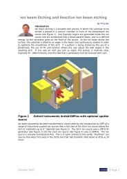
The basic DIBS (Dual <strong>Ion</strong> <strong>Beam</strong> Sputtering) chamber set up, see Figure 2 below, comprises a<br />
deposition source that accurately focuses a neutralised ion beam onto a target with minimal<br />
overspill so as to avoid contamination of depositing films. This enables materials such as Au,<br />
Cr, Ti, Pt for metal tracks, magnetic materials such as Fe, Co, Ni, etc. or dielectrics such as SiO 2 ,<br />
Al 2 O 3 , etc. to be deposited (the list is non-exhaustive).<br />
It also comprises an assist/etch source that can fulfil various functions: it can be used to etch<br />
(or ion mill) the substrate; it can provide “assistance” to the deposition process by<br />
bombarding the depositing film with energetic ions which can improve or modify the film<br />
properties or stoichiometry by physical and/or chemical effects; it can also be used as a lowenergy<br />
pre-clean of the substrate prior to deposition. Sometimes, this source is used without<br />
grids as a plasma source of ‘thermal’ activated radicals for chemical modification of the<br />
depositing material while minimising physical bombardment of the substrate.<br />
The <strong>Ion</strong>fab tool can also be supplied with only one or other of the above ion sources, either<br />
for deposition where assist or etch is not required for the process, or as an<br />
etching/milling/surface modification tool where no deposition is required.<br />
15cm <strong>Deposition</strong> source<br />
with focussed Grids<br />
Substrate holder<br />
15cm or 30cm<br />
Assist source with Grids<br />
Targets<br />
Source gas: Ar<br />
Chamber gas Ar, O 2 or N 2<br />
Source gas Ar, O 2 or N 2<br />
FIGURE 2 Schematic view of an <strong>Ion</strong>Fab system<br />
© Oxford Instruments Plasma Technology Ltd, 2010. All rights reserved.<br />
3
Results<br />
Some of the most common materials deposited are oxides such as Al 2 O 3 , Ta 2 O 5 , SiO 2 and TiO 2<br />
(usually from Al2O 3 , Ta, Si, SiO 2 and Ti targets and with O 2 added to the process gas). Indeed,<br />
O 2 can be introduced either directly into the chamber or through the deposition and/or the<br />
assist source; this allows stoichiometric dielectrics to be deposited either from a stochiometric<br />
dielectric target, where oxygen depletion during sputtering is replaced, or from a metal<br />
target in reactive mode where the sputtered metal atoms are oxidized at some point which<br />
could be on the target, during transit to the substrate or on the substrate if an oxygenbearing<br />
assist beam or plasma is used. The second source can also be used for substrate preclean<br />
to, for example, achieve improved adhesion of the films or remove native oxides, or as<br />
a physical assist during deposition to further densify the films.<br />
The same can be done for nitride deposition, e.g. Si 3 N 4 using a Si 3 N 4 target and N 2 in the<br />
chamber or assist source. Other, more ‘exotic’, materials, such as MgF 2 , LaF 3 , Nb 2 O 5 , ZrO 3 , Y 2 O 3 ,<br />
HfO 2 YF 3 etc., may also be deposited by (reactive and/or assisted) ion beam sputtering and the<br />
list includes such material as VO X that requires extremely precise control of process gas ratios<br />
to allow very specific thermo-electrical properties to be achieved for sensitive thermal<br />
imaging applications.<br />
Our tool also allows the substrate to be rotated and inclined relative to the sputter flux<br />
direction enabling further 'tuning' of film growth/properties as well as step coverage control<br />
for deposition onto surface topology. <strong>Deposition</strong> rates will be lower than evaporation, but<br />
this does allow much more control with a much more reproducible and predictable<br />
deposition rate allowing very precise thickness control simply by timing. The material is also<br />
sputtered and deposited in a much lower temperature environment than evaporation. The<br />
actual substrate temperature can thus be kept very low during processing using the helium<br />
fed back-side cooling capability.<br />
<strong>Ion</strong> beam deposition runs in a much lower pressure environment (in the 10 -4 Torr range or<br />
lower) than standard magnetron sputtering, so any sputter gas (e.g. Ar) inclusion in the film<br />
is much less of a problem (as is also true for evaporation). The mean free path of ions and<br />
sputtered material is accordingly greatly increased which also inhibits thermalisation of<br />
sputtered material as well, resulting in depositing atom kinetic energies (typically between 1<br />
to 100 eV) much higher than, for example, in the case of evaporated atoms,.<br />
Since substrate preparation and/or film stress are usually the cause of problems in adhesion<br />
for thicker films, ion beam deposition can provide both surface pre-clean and film stress<br />
control by the second ion source. Moreover, ion beam deposition does not suffer from the<br />
problem of 'spitting' often seen in evaporation.<br />
The deposited film qualities may be divided into optical and mechanical categories:<br />
Optical properties of a thin film are characterized by the following qualities:<br />
-Transmittance (associated with dispersive values and homogeneity)<br />
-Absorption (associated with transparency properties)<br />
-Scatter (associated with surface roughness and volume defects)<br />
Our dedicated ion beam optical coaters give good scatter loss results thanks to smooth film<br />
deposition. Figure 3 below shows some examples of single oxide layers of SiO 2 and TiO 2 on Si<br />
wafer. A surface roughness of 0.22nm rms for Si 3 N 4 deposited on a Si wafer has also been<br />
measured.<br />
© Oxford Instruments Plasma Technology Ltd, 2010. All rights reserved.<br />
4
SiO 2<br />
Rms=0.31nm<br />
TiO 2<br />
Rms=0.20nm<br />
FIGURE 3 Surface roughness evaluation measurements by AFM<br />
However, in addition to excellent film smoothness, the ion beam tool must have reliable and<br />
reproducible sources if the same results are to be obtained for the next film to be deposited.<br />
Both film thickness and refractive index reproducibility are very important when depositing<br />
multilayer coatings.<br />
In Figure 4 below is shown Ta 2 O 5 deposition over three consecutive runs measured over an 8”<br />
wafer deposited on a Si wafer. Figure 5 shows the corresponding refractive index<br />
repeatability obtained over the same three consecutive deposition runs. Figure 6 shows an<br />
example of Si 3 N 4 deposition uniformity over 100mm on Si wafer with a ±0.1% refractive index<br />
uniformity. Figure 7 shows an example of SiO 2 deposition uniformity over 200mm on Si wafer<br />
with better than ±0.1% refractive index uniformity with 5mm edge exclusion. It can be<br />
observed that the different profile of the curve compared to Ta 2 O 5 deposition is linked with<br />
the different platen positioning and beam parameters that affect beam divergence.<br />
FIGURE 4 Ta 2 O 5 deposition uniformity over three consecutive runs on 200mm Si wafer<br />
© Oxford Instruments Plasma Technology Ltd, 2010. All rights reserved.<br />
5
FIGURE 5 Repeatable dispersion for Ta 2 O 5 refractive index over three consecutive runs<br />
FIGURE 6 Si 3 N 4 deposition uniformity over 100mm on Si wafer<br />
© Oxford Instruments Plasma Technology Ltd, 2010. All rights reserved.<br />
6
FIGURE 7 SiO 2 deposition uniformity over 200mm on Si wafer<br />
Some examples are shown below of applications that our tools are being used for:<br />
Laser bar coating for individual bars on both facets: Dual wavelength anti-reflection (AR)<br />
coating parameters with an 8 layer Ta 2 O 5 /SiO 2 coating.<br />
Transmission @532nm: 99.815%<br />
Transmission @1064nm : 99.390%<br />
FIGURE 8 Anti Reflection coating (AR) coating with 8 layers coating Ta 2 O 5 /SiO 2 .<br />
Single cavity filter: in Figure 9 below can be seen the theoretical transmittance as<br />
calculated with MacLeod together with the as-deposited multilayer scan measured with a<br />
spectrophotometer<br />
Peak Insertion loss –0.08dB<br />
FWHM = 2.021nm<br />
Centre Wavelength: 1553.4 nm,<br />
40 QW’s<br />
© Oxford Instruments Plasma Technology Ltd, 2010. All rights reserved.<br />
7
FIGURE 9 Single cavity transmittance<br />
Three cavities mirror, Figure 10 below shows insertion loss scan versus wavelength.<br />
Centre Wavelength 1549.8nm (ITU = 1549.72nm)<br />
Pass Band Bandwidth (@ - 0.5dB) = 1.07nm<br />
Stop Band Bandwidth (@ - 25dB) = 2.7nm<br />
Insertion loss (@1549.7nm:193.45THz) = -0.086dB<br />
FIGURE 10 Insertion loss scan versus wavelength for a three cavities mirror<br />
Ring laser gyroscope (RLG), Figure 11 below shows transmission scan of a mirror<br />
designed for 633nm at 45°.<br />
Mirror loss
120<br />
100<br />
80<br />
Transmission (%)<br />
60<br />
40<br />
20<br />
0<br />
300 400 500 600 700 800 900 1000<br />
Wavelength (nm)<br />
FIGURE 11 Transmission scan of a mirror designed for 633nm at 45°<br />
Some of our customers have achieved total losses below 20 ppm for their ring laser gyroscope<br />
mirrors. Clean room environment and process optimization as well as system preparation are<br />
key in order for total losses to be kept to a minimum.<br />
The list of applications is extensive with only a few examples having been shown. Many types<br />
of multilayer coatings are feasible and, depending on the type of coating, throughput and<br />
quality required, various means can be provided for monitoring and controlling their growth<br />
such as quartz crystal monitors or in situ optical monitoring.<br />
Conclusion<br />
As has been seen above, the main benefits offered by ion beam deposition are:<br />
• High surface quality<br />
• Dense smooth films<br />
• Very low scattering<br />
• Very low optical losses<br />
• Very good run to run process repeatability<br />
• Excellent uniformity<br />
• Maximum flexibility<br />
• Range of applications<br />
© Oxford Instruments Plasma Technology Ltd, 2010. All rights reserved.<br />
9